AAT1143
1MHz 400mA Step-Down Converter
1143.2005.09.1.7
1
SwitchReg
TM
General Description
The AAT1143 SwitchRegTM is a member of
AnalogicTech's Total Power Management ICTM
(TPMICTM) product family. It is a 1MHz step-down
converter with an input voltage range of 2.7V to
5.5V and output as low as 0.6V. Its low supply cur-
rent, small size, and high switching frequency
make the AAT1143 the ideal choice for portable
applications.
The AAT1143 is available in either a fixed version
with internal feedback or a programmable version
with external feedback resistors. It can deliver
400mA of load current while maintaining a low
25µA no load quiescent current. The 1MHz switch-
ing frequency minimizes the size of external com-
ponents while keeping switching losses low. The
AAT1143 feedback and control delivers excellent
load regulation and transient response with a small
output inductor and capacitor.
The AAT1143 is designed to maintain high efficien-
cy throughout the operating range, which is critical
for portable applications.
The AAT1143 is available in a space-saving
2.0x2.1mm SC70JW-8 package and is rated over
the -40∞C to +85∞C temperature range.
Features
∑
V
IN
Range: 2.7V to 5.5V
∑
V
OUT
Adjustable Down to 0.6V
-- Fixed or Adjustable Version
∑
25µA No Load Quiescent Current
∑
Up to 95% Efficiency
∑
400mA Max Output Current
∑
1MHz Switching Frequency
∑
Soft Start
∑
Over-Temperature Protection
∑
Current Limit Protection
∑
100% Duty Cycle Low-Dropout Operation
∑
0.1µA Shutdown Current
∑
SC70JW-8 Package
∑
Temperature Range: -40∞C to +85∞C
Applications
∑
Cellular Phones
∑
Digital Cameras
∑
Handheld Instruments
∑
Microprocessor / DSP Core / IO Power
∑
PDAs and Handheld Computers
∑
USB Devices
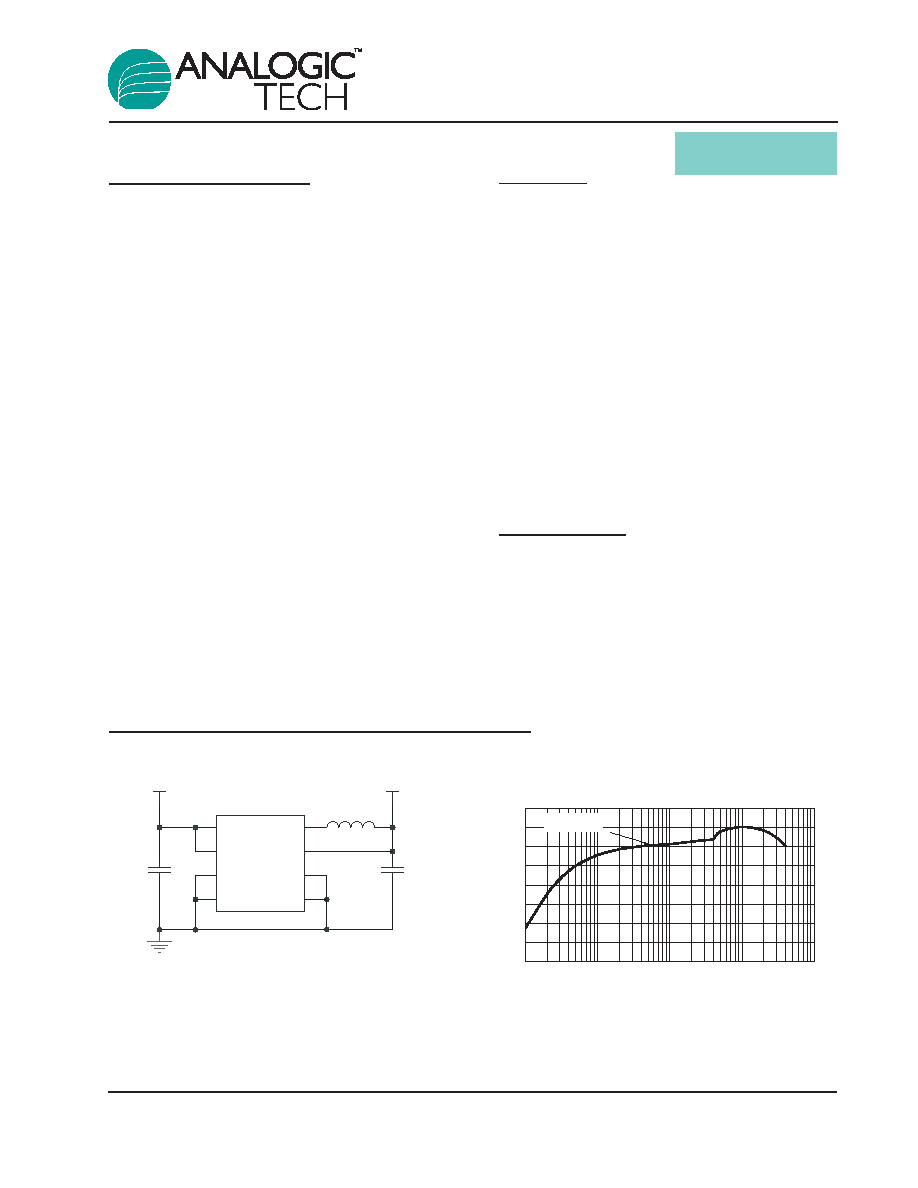
Typical Application (Fixed Output Voltage)
AAT1143 Efficiency
(V
OUT
= 2.5V; L = 4.7
µ
µH)
Output Current (mA)
Efficiency (%)
60
70
80
90
100
0.1
1
10
100
1000
V
IN
= 3.3V
4.7
µH
L1
4.7
µF
C1
4.7
µF
C2
EN
1
OUT
2
VIN
3
LX
4
AGND
5
PGND
6
PGND
7
PGND
8
AAT1143
U1
V
IN
V
O

Pin Descriptions
Pin Configuration
SC70JW-8
(Top View)
OUT
VIN
LX
PGND
PGND
PGND
AGND
EN
1
2
3
4
5
6
7
8
Pin #
Symbol
Function
1
EN
Enable pin.
2
OUT
Feedback input pin. This pin is connected either directly to the converter
output or to an external resistive divider for an adjustable output.
3
VIN
Input supply voltage for the converter.
4
LX
Switching node. Connect the inductor to this pin. It is internally connected to
the drain of both high- and low-side MOSFETs.
5
AGND
Non-power signal ground pin.
6, 7, 8
PGND
Main power ground return pin. Connect to the output and input capacitor
return.
AAT1143
1MHz 400mA Step-Down Converter
2
1143.2005.09.1.7
Absolute Maximum Ratings
1
Thermal Information
Symbol
Description
Value
Units
P
D
Maximum Power Dissipation (SC70JW-8)
625
mW
JA
Thermal Resistance
2
(SC70JW-8)
160
∞C/W
Symbol
Description
Value
Units
V
IN
Input Voltage GND
6.0
V
V
LX
L
X
to GND
-0.3 to V
P
+ 0.3
V
V
OUT
OUT to GND
-0.3 to V
P
+ 0.3
V
V
EN
EN to GND
-0.3 to 6.0
V
T
J
Operating Junction Temperature Range
-40 to 150
∞C
T
LEAD
Maximum Soldering Temperature (at leads, 10 sec)
300
∞C
AAT1143
1MHz 400mA Step-Down Converter
1143.2005.09.1.7
3
1. Stresses above those listed in Absolute Maximum Ratings may cause permanent damage to the device. Functional operation at condi-
tions other than the operating conditions specified is not implied. Only one Absolute Maximum Rating should be applied at any one time.
2. Mounted on an FR4 board.
Electrical Characteristics
1
T
A
= -40∞C to +85∞C, unless otherwise noted. Typical values are T
A
= 25∞C, V
IN
= 3.6V.
Symbol
Description
Conditions
Min
Typ
Max Units
Step-Down Converter
V
IN
Input Voltage
2.7
5.5
V
V
IN
Rising
2.6
V
V
UVLO
UVLO Threshold
Hysteresis
100
mV
V
IN
Falling
1.8
V
V
OUT
Output Voltage Tolerance
I
OUT
= 0 to 400mA,
-3.0
+3.0
%
V
IN
= 2.7V to 5.5V
V
OUT
Output Voltage Range
Fixed Output Version
0.6
4.0
V
Adjustable Output Version
2
0.6
2.5
I
Q
Quiescent Current
No Load, 0.6V Adjustable
25
50
µA
Version
I
SHDN
Shutdown Current
EN = AGND = PGND
1.0
µA
I
LIM
P-Channel Current Limit
600
mA
R
DS(ON)H
High Side Switch On Resistance
0.45
R
DS(ON)L
Low Side Switch On Resistance
0.40
I
LXLEAK
LX Leakage Current
V
IN
= 5.5V, V
LX
= 0 to V
IN
,
1
µA
EN = GND
V
Linereg
Line Regulation
V
IN
= 2.7V to 5.5V
0.2
%/V
V
OUT
Out Threshold Voltage Accuracy
0.6V Output, No Load
597
600
615
mV
T
A
= 25∞C
I
OUT
Out Leakage Current
0.6V Output
0.2
µA
R
OUT
Out Impedance
>0.6V Output
250
k
F
OSC
Oscillator Frequency
T
A
= 25∞C
0.7
1.0
1.5
MHz
T
SD
Over-Temperature Shutdown Threshold
140
∞C
T
HYS
Over-Temperature Shutdown Hysteresis
15
∞C
EN
V
EN(L)
Enable Threshold Low
0.6
V
V
EN(H)
Enable Threshold High
1.4
V
I
EN
Input Low Current
V
IN
= V
FB
= 5.5V
-1.0
1.0
µA
AAT1143
1MHz 400mA Step-Down Converter
4
1143.2005.09.1.7
1. The AAT1143 is guaranteed to meet performance specifications over the -40∞C to +85∞C operating temperature range and is assured
by design, characterization, and correlation with statistical process controls.
2. For adjustable version with higher than 2.5V output, please consult your AnalogicTech representative.
INTERNAL DOCUMENT
DO NOT COPY
AAT1143
1MHz 400mA Step-Down Converter
1143.2005.09.1.7
5
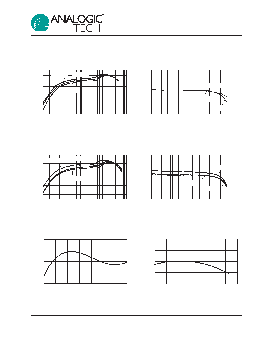
Typical Characteristics
Output Voltage Error vs. Temperature
(V
IN
= 3.6V; V
O
= 1.5V)
Temperature (
∞
∞C)
Output Error (%)
-2.0
-1.0
0.0
1.0
2.0
-40
-20
0
20
40
60
80
100
Frequency vs. Input Voltage
(V
OUT
= 1.8V)
Input Voltage (V)
Frequency Variation (%)
-2.0
-1.5
-1.0
-0.5
0.0
0.5
1.0
2.7
3.1
3.5
3.9
4.3
4.7
5.1
5.5
DC Regulation
(V
OUT
= 1.8V; L = 4.7
µ
µH)
Output Current (mA)
Output Error (%)
-2.0
-1.0
0.0
1.0
2.0
0.1
1
10
100
1000
V
IN
= 2.7V
V
IN
= 3.6V
V
IN
= 4.2V
Efficiency vs. Load
(V
OUT
= 1.8V; L = 4.7
µ
µH)
Output Current (mA)
Efficiency (%)
50
60
70
80
90
100
0.1
1
10
100
1000
V
IN
= 2.7V
V
IN
= 3.6V
V
IN
= 4.2V
Load Regulation
(V
OUT
= 2.5V; L = 4.7
µ
µH)
Output Current (mA)
Output Error (%)
-2.0
-1.0
0.0
1.0
2.0
0.1
1
10
100
1000
V
IN
= 3.0V
V
IN
= 3.3V
V
IN
= 3.6V
Efficiency vs. Load
(V
OUT
= 2.5V; L = 4.7
µ
µH)
Output Current (mA)
Efficiency (%)
60
70
80
90
100
0.1
1
10
100
1000
V
IN
= 3.3V
V
IN
= 3.6V
V
IN
= 3.0V