
SwitchReg
TM
AAT1152
850kHz 1A Synchronous Buck DC/DC Converter
Preliminary Information
1152.2003.01.0.9
1
General Description
The AAT1152 SwitchRegTM is a member of
AnalogicTechTM's Total Power ManagementTM IC
product family. The Step-down switching converter
is ideal for applications where high efficiency, small
size, and low ripple are critical. Able to deliver 1A
with internal Power MOSFETs, the current-mode
controlled IC provides high efficiency using syn-
chronous rectification. Fully internally compensat-
ed, the AAT1152 simplifies system design and low-
ers external part count.
The AAT1152 features a Power Good (POK) func-
tion which monitors the output, alerting the system
if the output voltage falls out of regulation.
The AAT1152 is available in MSOP-8 package,
rated over -40 to 85∞C.
Features
∑
5.5V max supply input
∑
Fixed output voltage: 1.1V≠4.2V with 100 mV
increment
∑
1A output current
∑
Integrated low on resistance power switches
∑
Synchronous rectification
∑
Up to 95% efficiency
∑
Power Good signal
∑
Internally compensated current mode control
∑
High initial accuracy: ±1%
∑
850kHz switching frequency
∑
Constant PWM mode
∑
Low output ripple with light load
∑
Internal softstart
∑
Current limit protection
∑
Over-Temperature protection
∑
MSOP-8 package
Applications
∑
Computer Peripherals
∑
Set Top Boxes
∑
Network Cards
∑
Cable/DSL Modems
∑
High efficiency conversion from 5V or 3.3V
supply
Typical Application
OUTPUT
4.1
µ
H
47
µ
F
10
µ
F
0.1
µ
F
100
LX
100k
V
P
INPUT
FB
SGND
AAT1152
ENABLE
POK
V
CC
P
GND
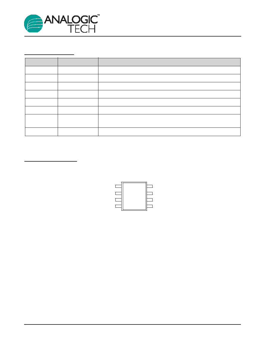
AAT1152
850kHz 1A Synchronous Buck DC/DC Converter
2
1152.2003.01.0.9
Pin Descriptions
Pin Configuration
MSOP-8
1
2
POK
P
GND
LX
V
P
FB
SGND
EN
V
CC
1
2
3
4
8
7
6
5
Pin #
Symbol
Function
1
FB
Feedback input pin
2
SGND
Signal Ground
3
EN
Converter enable pin
4
V
CC
Small Signal Filtered Bias Supply
5
V
P
Input supply for converter power stage
6
LX
Inductor connection pin
7
POK
Power Good indicator. Open-drain output is low when V
OUT
falls
out of regulation.
8
PGND
Power ground return for output stage
AAT1152
850kHz 1A Synchronous Buck DC/DC Converter
1152.2003.01.0.9
3
Absolute Maximum Ratings
(T
A
=25∞C unless otherwise noted)
Note: Stresses above those listed in Absolute Maximum Ratings may cause permanent damage to the device. Functional operation at con-
ditions other than the operating conditions specified is not implied. Only one Absolute Maximum rating should be applied at any one time.
Note 1: Human body model is a 100pF capacitor discharged through a 1.5K resistor into each pin.
Thermal Characteristics
Note 2: Mounted on a demo board.
Recommended Operating Conditions
Symbol
Description
Rating
Units
T
Ambient Temperature Range
-40 to +85
∞C
Symbol
Description
Value
Units
JA
Maximum Thermal Resistance (MSOP-8)
2
150
∞C/W
P
D
Maximum Power Dissipation (MSOP-8)
2
833
mW
Symbol
Description
Value
Units
V
CC
, V
P
V
CC
, V
P
to GND
6
V
V
LX
LX to GND
-0.3 to V
P
+0.3
V
V
FB
FB to GND
-0.3 to V
CC
+0.3
V
V
EN
, V
POK
POK, EN to GND
-0.3 to 6
V
T
J
Operating Junction Temperature Range
-40 to 150
∞C
T
LEAD
Maximum Soldering Temperature (at leads, 10 sec)
300
∞C
V
ESD
ESD Rating
1
- HBM
3000
V

Electrical Characteristics
(V
IN
= V
CC
= V
P
= 5V, T
A
= -40 to 85∞C unless otherwise noted. Typical
values are at T
A
= 25∞C)
Symbol
Description
Conditions
Min
Typ
Max
Units
V
IN
Operation Voltage
2.7
5.5
V
V
OUT
DC Output Voltage Tolerance
I
OUT
= 500mA
T
A
= 25∞C
-1.0
+1.0
%
Full temp
-2.0
+2.0
I
LIM
Current Limit
T
A
= 25∞C
1.2
A
I
Q
Quiescent Supply Current
No load, V
FB
= 0
160
300
µA
V
OUT
(V
OUT
*
V
IN
) Load Regulation
V
IN
= 4.2V, I
LOAD
= 0 to 1A
3
%
V
OUT
/V
OUT
Line Regulation
V
IN
= 2.7 to 5.5V
0.2
%/V
F
OSC
Oscillator frequency
T
A
= 25∞C
700
850
1000
kHz
R
DSON(H)
High-side Switch On-resistance
T
A
= 25∞C
110
150
m
R
DSON(L)
Low-side Switch On-resistance
T
A
= 25∞C
100
150
m
V
EN(H)
Enable input high voltage
V
IN
= 2.7 to 5.5V
1.4
V
V
EN(L)
Enable input low voltage
V
IN
= 2.7 to 5.5V
0.6
V
I
EN
Enable Pin Leakage Current
V
EN
= 5.5V
1
µA
V
UVLO
Undervoltage Lockout
V
IN
rising
2.5
V
V
IN
falling
1.2
V
UVLO(hys)
Undervoltage Lockout Hysteresis
250
mV
T
SD
Over Temp Shutdown Threshold
140
∞C
T
HYS
Over Temp Shutdown Hysteresis
15
∞C
I
SHDN
Shutdown current
V
EN
= 0, V
IN
= 5.5V
1
µA
V
TH(POK)
Power Good Threshold
V
FB
Ramping Up
90
% of
V
FB
Ramping Down
88
V
FB
R
POK
Power Good Pull-Down
4
On-Resistance
AAT1152
850kHz 1A Synchronous Buck DC/DC Converter
4
1152.2003.01.0.9

AAT1152
850kHz 1A Synchronous Buck DC/DC Converter
1152.2003.01.0.9
5
Typical Characteristics
Oscillator Frequency Variation vs. Temperature
V
IN
=3.6V
-10
-6
-2
2
6
10
-20
0
20
40
60
80
100
Temperature (
∞
C)
Variation (%)
Oscillator Frequency Variation vs.
Supply Voltage
-1.5
-0.5
0.5
1.5
2.5
3.5
2.5
3
3.5
4
4.5
5
5.5
Supply Voltage (V)
Variation (%)
Enable Threshold vs. Input Voltage
0.7
0.8
0.9
1
1.1
1.2
2.5
3
3.5
4
4.5
5
5.5
Input Voltage (V)
Enable Threshold (V)
V
EN
(H)
V
EN
(L)
R
DS(ON)
vs. Input Voltage
80
90
100
110
120
130
2.5
3
3.5
4
4.5
5
5.5
Input Voltage (V)
R
DS(ON)
(m
)
High Side
Low Side
Low Side R
DS(ON)
vs. Temperature
70
90
110
130
150
170
-20
0
20
40
60
80
100
120
Temperature (
∞
C)
R
DS(ON)
(m
)
2.7V
3.6V
4.2V
5.5V
High Side R
DS(ON)
vs. Temperature
70
90
110
130
150
170
-20
0
20
40
60
80
100
120
Temperature (
∞
C)
R
DS(ON)
(m
)
2.7V
3.6V
4.2V
5.5V