SwitchReg
TM
AAT1154
1MHz 3A Buck DC/DC Converter
Preliminary Information
1154.2003.08.0.91
1
General Description
The AAT1154 SwitchRegTM is a member of
AnalogicTechTM's Total Power ManagementTM IC
product family. The Step-down switching converter
is ideal for applications where high efficiency, small
size, and low ripple are critical. Able to deliver 3A
with an internal power MOSFET, the current-mode
controlled IC provides high efficiency. Fully inter-
nally compensated, the AAT1154 simplifies system
design and lowers external part count.
The AAT1154 is available in an SOP-8 package,
rated over -40 to 85∞C.
Features
∑
V
IN
Range: 2.7-5.5Volts
∑
Fixed or adjustable V
OUT
: 1.0V - 4.2V
∑
3A output current
∑
Up to 95% efficiency
∑
Integrated low on resistance power switch
∑
Internally compensated current mode control
∑
1MHz switching frequency
∑
Constant PWM mode
∑
Low output ripple with light load
∑
Internal softstart
∑
Current limit protection
∑
Over-Temperature protection
∑
SOP-8 package
∑
-40 to 85∞C Temperature Range
Applications
∑
Computer Peripherals
∑
Set Top Boxes
∑
Network Cards
∑
Cable/DSL Modems
∑
High efficiency conversion from 5V or 3.3V
supply
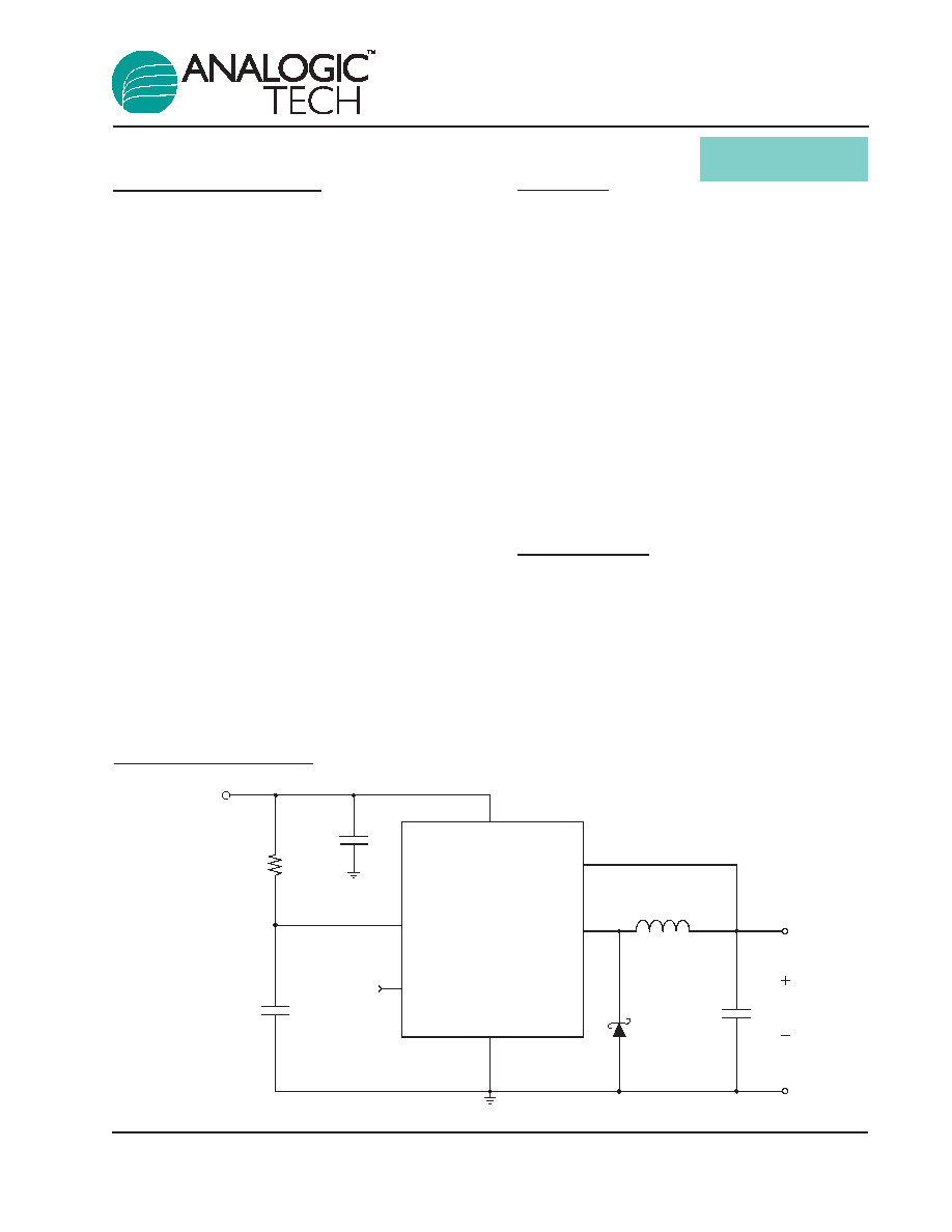
Typical Application
OUTPUT
INPUT
1.5
µ
H
120
µ
F
LX
V
P
FB
GND
AAT1154
V
CC
ENABLE
10
µ
F
0.1
µ
F
100
AAT1154
1MHz 3A Buck DC/DC Converter
2
1154.2003.08.0.91
Pin Descriptions
Pin Configuration
SO-8
1
2
LX
V
P
LX
V
P
FB
GND
EN
V
CC
1
2
3
4
8
7
6
5
Pin #
Symbol
Function
1
FB
Feedback input pin. This pin must be connected to the converter's
output. It is used to set the output of the converter to regulate to the
desired value.
2
GND
Ground connection.
3
EN
Enable input pin. When connected high, AAT1154 is in normal
operation. When connected low, it is powered down. This pin
should not be left floating.
4
VCC
Power supply. It supplies power for the internal circuitry.
5, 8
VP
Input Supply Voltage for converter power stage.
6, 7
LX
Inductor connection pins. These pins should be connected to the
output inductor. Internally, pins 6 & 7 are connected to the drain of
the P-channel switch.
AAT1154
1MHz 3A Buck DC/DC Converter
1154.2003.08.0.91
3
Absolute Maximum Ratings
(T
A
=25∞C unless otherwise noted)
Note: Stresses above those listed in Absolute Maximum Ratings may cause permanent damage to the device. Functional operation at con-
ditions other than the operating conditions specified is not implied. Only one Absolute Maximum rating should be applied at any one time.
Note 1: Human body model is a 100pF capacitor discharged through a 1.5K resistor into each pin.
Thermal Characteristics
Note 2: Mounted on a demo board (FR4, in still air).
Note 3: Derate 9.1mW/∞C above 25∞C.
Recommended Operating Conditions
Symbol
Description
Rating
Units
T
Ambient Temperature Range
-40 to +85
∞C
Symbol
Description
Value
Units
JA
Thermal Resistance
2
110
∞C/W
P
D
Maximum Power Dissipation (T
A
= 25∞C)
2, 3
909
mW
Symbol
Description
Value
Units
V
CC
, V
P
V
CC
, V
P
to GND
6
V
V
LX
LX to GND
-0.3 to V
P
+0.3
V
V
FB
FB to GND
-0.3 to V
CC
+0.3
V
V
EN
EN to GND
-0.3 to V
CC
+0.3
V
T
J
Operating Junction Temperature Range
-40 to 150
∞C
V
ESD
ESD Rating
1
- HBM
3000
V
Electrical Characteristics
(V
IN
= V
CC
= V
P
= 5V, T
A
= -40 to 85∞C unless otherwise noted. Typical
values are at T
A
= 25∞C)
Symbol
Description
Conditions
Min Typ Max Units
V
IN
Input Voltage Range
2.7
5.5
V
V
OUT
Output Voltage Tolerance
V
IN
= V
OUT
+ 0.2 to 5.5V,
-5.0
5.0
%
I
OUT
= 0 to 3A
V
UVLO
Under Voltage Lockout
V
IN
Rising
2.5
V
V
IN
Falling
1.2
V
V
UVLO(HYS)
Under Voltage Lockout Hysteresis
250
mV
I
Q
Quiescent Supply Current
No Load, V
FB
= 0 V
630 1000
µA
I
SHDN
Shutdown Current
V
EN
= 0 V, V
IN
= 5.5V
1.0
µA
I
LIM
Current Limit
T
A
= 25∞C
4.4
A
R
DS(ON)L
High Side Switch On Resistance
T
A
= 25∞C
60
m
Efficiency
I
OUT
= 1.0 A
92
V
OUT
(V
OUT
*
V
IN
) Load Regulation
I
LOAD
= 0 - 3A
±
2.6
%
V
OUT
/V
OUT
Line Regulation
V
IN
= 2.7 to 5.5V
0.75
%/V
F
OSC
Oscillator Frequency
T
A
= 25∞C
1
MHz
V
EN(L)
Enable Threshold Low
0.6
V
V
EN(H)
Enable Threshold High
1.4
V
T
SD
Over Temp Shutdown Threshold
140
∞C
T
HYS
Over Temp Shutdown Hysteresis
15
∞C
AAT1154
1MHz 3A Buck DC/DC Converter
4
1154.2003.08.0.91
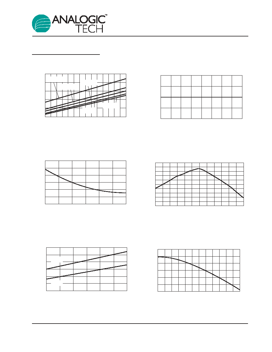
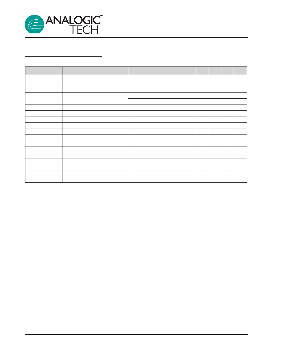
Typical Characteristics
Output Voltage vs. Temperature
I
OUT
=2A
-20
0
20
40
60
80
100
Temperature (
∞
∞
C)
Variation (%)
-0.8
-0.6
-0.4
-0.2
0
0.2
0.4
Enable Threshold vs. Input Voltage
0.6
0.7
0.8
0.9
1
1.1
1.2
2.5
3
3.5
4
4.5
5
5.5
Input Voltage (V)
Enable Threshold (V)
EN(H)
EN(L)
Oscillator Frequency Variation vs. Temperature
V
IN
= 5V
-4
-3
-2
-1
0
1
-20
0
20
40
60
80
100
Temperature (
∞
C)
Variation (%)
R
DS(ON)
vs. V
IN
, I
DS
= 1A
40
45
50
55
60
65
70
2.5
3
3.5
4
4.5
5
5.5
Input Voltage (V)
R
DS(ON)
(m
)
Oscillator Frequency Variation vs.
Supply Voltage
-0.5
-0.25
0
0.25
0.5
3.5
4
4.5
5
5.5
Input Voltage (V)
Variation (%)
R
DS(ON)
vs. Temperature
40
50
60
70
80
90
-20
0
20
40
60
80
100
120
Temperature (
∞
C)
R
DS(ON)
(m
)
V
IN
= 2.7V
V
IN
= 3.6V
V
IN
= 4.2V
V
IN
= 5V
V
IN
= 5.5V
AAT1154
1MHz 3A Buck DC/DC Converter
1154.2003.08.0.91
5