AAT1156
1MHz 700mA Step-Down DC-DC Converter
1156.2005.11.1.2
1
SwitchReg
TM
General Description
The AAT1156 SwitchRegTM is a member of
AnalogicTechTM's Total Power Management ICTM
(TPMICTM) product family. The step-down switching
converter is ideal for applications where high effi-
ciency is required over the full range of load condi-
tions. The 2.7V to 5.5V input voltage range makes
the AAT1156 ideal for single-cell lithium-ion/polymer
battery applications. Capable of more than 700mA
with internal MOSFETs, the current-mode con-
trolled IC provides high efficiency over a wide oper-
ating range. Fully integrated compensation simpli-
fies system design and lowers external parts count.
The AAT1156 is available in the 16-pin 3x3mm
QFN package and is rated over the -40∞C to +85∞C
temperature range.
Features
∑
V
IN
Range: 2.7 to 5.5 Volts
∑
Up to 95% Efficiency
∑
110m
R
DS(ON)
Internal Switches
∑
<1µA Shutdown Current
∑
1MHz Step-Down Switching Frequency
∑
Fixed or Adjustable V
OUT
0.8V
∑
Integrated Power Switches
∑
Current Mode Operation
∑
Internal Compensation
∑
Stable with Ceramic Capacitors
∑
Internal Soft Start
∑
Over-Temperature Protection
∑
Current Limit Protection
∑
16-Pin QFN 3x3mm Package
∑
-40∞C to +85∞C Temperature Range
Applications
∑
Cellular Phones
∑
Digital Cameras
∑
MP3 Players
∑
Notebook Computers
∑
PDAs
∑
Wireless Notebook Adapters
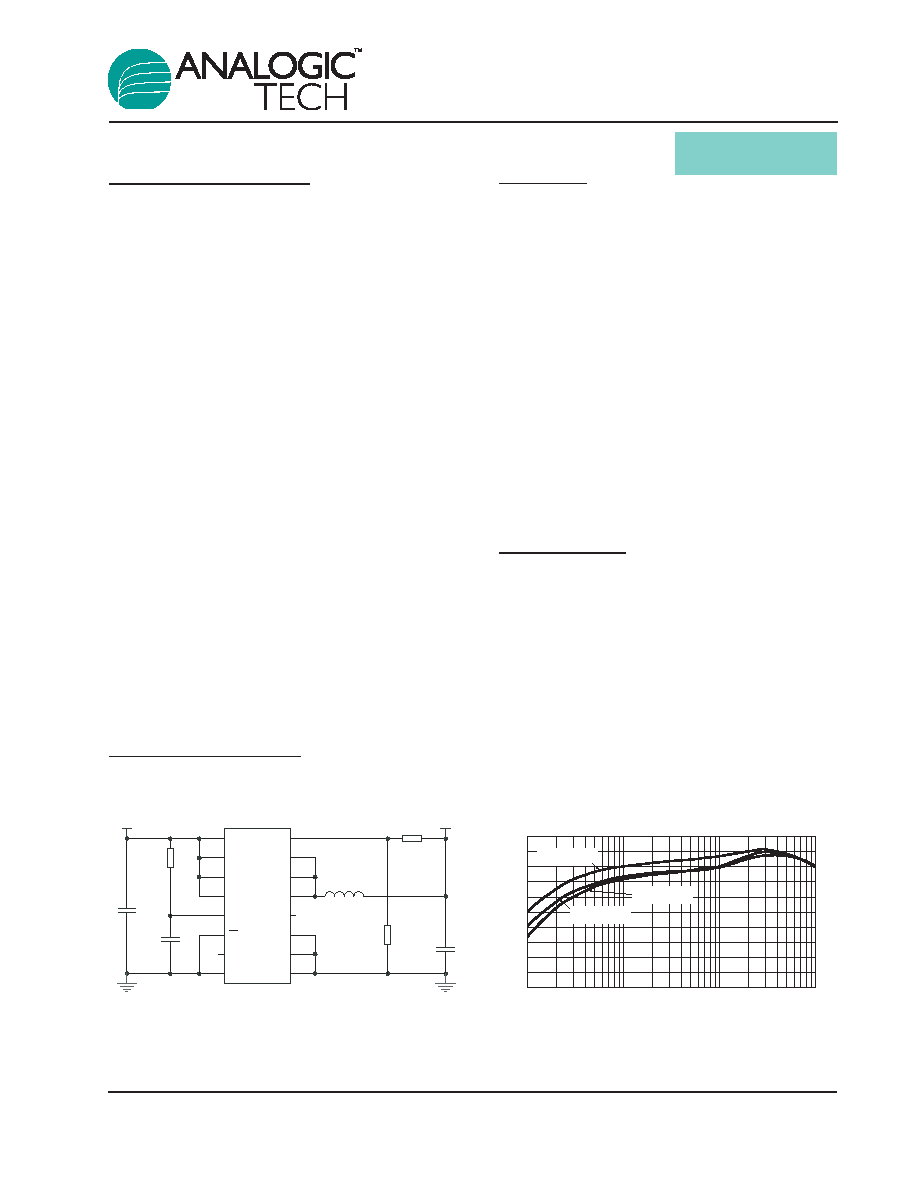
Typical Application
AAT1156 Efficiency
(V
OUT
= 2.5V; L = 4.7
µ
µH; CDRH3D16)
Output Current (mA)
Efficiency (%)
50
55
60
65
70
75
80
85
90
95
100
1
10
100
1000
V
IN
= 3.0V
V
IN
= 3.6V
V
IN
= 4.2V
4.7
µH
L1
2 x 22
µF
C3, C4
10
µF
C1
100
R1
0.1
µF
C2
C1 Murata 10
µF 6.3V X5R GRM42-6X5R106K6.3
C3-C4 MuRata 22
µF 6.3V GRM21BR60J226ME39L X5R 0805
2.5V
INPUT
L1 Sumida CDRH3D16-4R7NC
187k
R3
59k
R4
LX
14
LL
6
EN
7
VCC
9
VP
10
NC
8
LX
13
PGND
3
VP
12
VP
11
FB
4
LX
15
PGND
2
PGND
1
SGND
5
NC
16
AAT1156
U1
Pin Descriptions
Pin Configuration
QFN33-16
(Top View)
VP
VP
VP
NC
PGND
PGND
PGND
1
2
3
4
LL
SGND
EN
16
15
14
13
5
6
7
8
12
11
10
9
NC
VCC
LX
LX
LX
FB
Pin #
Symbol
Function
1, 2, 3
PGND
Main power ground return pin. Connect to the output and input capacitor
return. (See board layout rules.)
4
FB
Feedback input pin. This pin is connected to the converter output. It is
used to set the output of the converter to regulate to the desired value
via an internal resistive divider. For an adjustable output, an external
resistive divider is connected to this pin on the 1V model.
5
SGND
Signal ground. Connect the return of all small signal components to this
pin. (See board layout rules.)
6
LL
Mode selector switch. When pulled low, the device enters light load mode.
7
EN
Enable input pin. A logic high enables the converter; a logic low forces
the AAT1156 into shutdown mode, reducing the supply current to less
than 1µA. The pin should not be left floating.
8, 16
NC
Not internally connected.
9
VCC
Bias supply. Supplies power for the internal circuitry. Connect to input
power via low pass filter with decoupling to SGND.
10, 11, 12
VP
Input supply voltage for the converter power stage. Must be closely
decoupled to PGND.
13, 14, 15
LX
Connect inductor to these pins. Switching node internally connected to
the drain of both high- and low-side MOSFETs.
EP
Exposed paddle (bottom); connect to PGND directly beneath package.
AAT1156
1MHz 700mA Step-Down DC-DC Converter
2
1156.2005.11.1.2
Absolute Maximum Ratings
1
Thermal Characteristics
Recommended Operating Conditions
Symbol
Description
Value
Units
T
Ambient Temperature Range
-40 to 85
∞C
Symbol
Description
Value
Units
JA
Maximum Thermal Resistance (QFN33-16)
3
50
∞C/W
P
D
Maximum Power Dissipation (QFN33-16)
4
(T
A
= 25∞C)
2.0
W
Symbol
Description
Value
Units
V
CC
, V
V
CC
, V
P
to GND
6
V
V
LX
LX to GND
-0.3 to V
P
+0.3
V
V
FB
FB to GND
-0.3 to V
CC
+0.3
V
V
EN
EN to GND
-0.3 to 6
V
T
J
Operating Junction Temperature Range
-40 to 150
∞C
V
ESD
ESD Rating
2
- HBM
3000
V
AAT1156
1MHz 700mA Step-Down DC-DC Converter
1156.2005.11.1.2
3
1. Stresses above those listed in Absolute Maximum Ratings may cause damage to the device. Functional operation at conditions other
than the operating conditions specified is not implied. Only one Absolute Maximum Rating should be applied at any one time.
2. Human body model is 100pF capacitor discharged through a 1.5k
resistor into each pin.
3. Mounted on a demo board (FR4, in still air).
4. Derate 20mW/∞C above 25∞C.
Electrical Characteristics
V
IN
= V
CC
= V
P
= 5V, T
A
= -40∞C to +85∞C, unless otherwise noted. Typical values are at T
A
= 25∞C.
Symbol
Description
Conditions
Min
Typ
Max Units
V
IN
Input Voltage Range
2.7
5.5
V
V
OUT
Output Voltage Tolerance
V
IN
= V
OUT
+ 0.2 to 5.5V,
-3
3
%
I
OUT
= 0 to 700mA
V
IL
Input Low Voltage
0.6
V
V
IH
Input High Voltage
1.4
V
V
UVLO
Under-Voltage Lockout
V
IN
Rising, V
EN
= V
CC
2.5
V
V
IN
Falling, V
EN
= V
CC
1.2
V
UVLO(HYS)
Under-Voltage Lockout Hysteresis
250
mV
I
IL
Input Low Current
V
IN
= V
FB
= 5.5V
1.0
µA
I
IH
Input High Current
V
IN
= V
FB
= 0V
1.0
µA
I
Q
Quiescent Supply Current
No Load, LL = 0V; V
FB
= 0V,
220
350
µA
V
IN
= 4.2V, T
A
= 25∞C
I
SHDN
Shutdown Current
V
EN
= 0V, V
IN
= 5.5V
1.0
µA
I
LIM
Current Limit
T
A
= 25∞C
1.2
A
R
DS(ON)H
High Side Switch On Resistance
T
A
= 25∞C
110
150
m
R
DS(ON)L
Low Side Switch On Resistance
T
A
= 25∞C
100
150
m
V
OUT
(V
OUT
*
V
IN
) Load Regulation
V
IN
= 4.2V, I
LOAD
= 0 to 700mA
±0.9
%
DV
OUT
/V
OUT
Line Regulation
V
IN
= 2.7 to 5.5V
±0.1
%/V
F
OSC
Oscillator Frequency
T
A
= 25∞C
750
1000
1350
kHz
T
SD
Over-Temperature Shutdown
140
∞C
Threshold
T
HYS
Over-Temperature Shutdown
15
∞C
Hysteresis
AAT1156
1MHz 700mA Step-Down DC-DC Converter
4
1156.2005.11.1.2
Typical Characteristics
No Load Supply Current vs. Input Voltage
Input Voltage (V)
Supply Current (
µ
µ
A)
0
50
100
150
200
250
300
2.5
3
3.5
4
4.5
5
5.5
-40
∞C
25
∞C
85
∞C
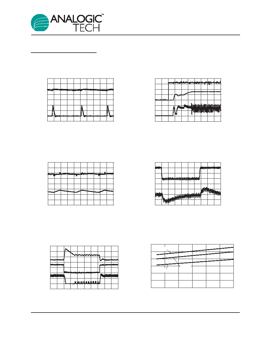
Load Transient Response
(50mA-680mA; V
IN
= 3.6V; V
OUT
= 0.8V)
Output Voltage
(top) (20mV/div)
Time (10
µ
µsec/div)
Inductor and Load Current
(bottom) (500mA/div)
0.67
0.69
0.71
0.73
0.75
0.77
0.79
0.81
0.83
ÿ
ÿ
Line Transient
(I
OUT
= 500mA; V
O
= 0.8V)
Input Voltage
(top) (V)
Output Voltage (AC coupled)
(bottom) (mV)
2.8
3
3.2
3.4
3.6
3.8
4
4.2
4.4
-20
-10
0
10
20
30
40
50
60
Time (20
µsec/div)
Output Ripple
(0.8V; 700mA; V
IN
= 3.6V)
Time (250ns/div)
Output Voltage
(AC coupled) (top) (mV)
Inductor Current
(bottom) (A)
-60
-50
-40
-30
-20
-10
0
10
20
-0.5
0
0.5
1
1.5
2
2.5
3
3.5
Soft Start
(0.8V; 700mA; V
IN
= 3.6V)
Time (100
µ
µs/div)
Enable and Output Voltage
(top) (V)
Inductor Current
(bottom) (A)
-2
-1.5
-1
-0.5
0
0.5
1
1.5
2
-0.5
0
0.5
1
1.5
2
2.5
3
3.5
Output Ripple
(0.8V; 10mA; V
IN
= 3.6V)
Time (2
µ
µs/div)
Output Voltage
(AC coupled) (top) (mV)
Inductor Current
(bottom) (A)
-60
-50
-40
-30
-20
-10
0
10
20
-0.2
0
0.2
0.4
0.6
0.8
1
1.2
1.4
AAT1156
1MHz 700mA Step-Down DC-DC Converter
1156.2005.11.1.2
5