
AAT3111
MicroPowerTM Regulated Charge Pump
Preliminary
Information
3111.2002.3.0.91
1
ChargePump
TM
General Description
The AAT3111 ChargePumpTM is a MicroPower
switched-capacitor voltage converter that delivers
a regulated output. No external inductor is required
for operation. Using three small capacitors, the
AAT3111 can deliver up to 150mA to the voltage
regulated output. The AAT3111 features very low
quiescent current and high efficiency over a large
portion of its load range making this device ideal
for battery-powered applications. Furthermore, the
combination of few external components and small
package size keeps the total converter board area
to a minimum in space restricted applications. The
AAT3111 operates in an output-regulated voltage
doubling mode. The regulator uses a pulse-skip-
ping technique to provide a regulated output from a
varying input supply. The AAT3111 contains a ther-
mal management circuit to protect the device
under continuous output short circuit conditions.
The AAT3111 is available in a surface mount 6-pin
SOT23 or 8-pin SC70JW package and is rated
from -40 to 85∞C.
The AAT3111 ChargePumpTM is a member of
AnalogicTech's Total Power Management IC prod-
uct family.
Features
∑
Step-up type voltage converter
∑
Input Range
∑
AAT3111-3.6: 1.8V to 3.6V
∑
AAT3111-3.3: 1.8V to 3.3V
∑
MicroPower consumption: 20µA
∑
3.6V, 3.3V Regulated ±4% output
∑
3.6V Output Current
∑
100mA with V
IN
3.0V
∑
20mA with V
IN
2.0V
∑
3.3V Output Current
∑
100mA with V
IN
2.5V
∑
20mA with V
IN
1.8V
∑
High Frequency 750 kHz operation
∑
Shutdown mode draws less than 1µA
∑
Short-circuit/over-temperature protection
∑
2kV ESD Rating
∑
SC70JW-8 or SOT23-6 package
Applications
∑
Handheld Electronics
∑
Digital Cameras
∑
PDAs
∑
Battery Back Up Supplies
∑
MP3 Players
Typical Application
V
IN
V
OUT
GND
SHDN
C+
V
IN
C-
AAT3111
V
OUT
1uF
10uF
10uF
ON/OFF
C
OUT
C
IN

Pin Descriptions
Pin Configuration
SOT23-6
SC70JW-8
1
2
GND
GND
GND
C+
V
IN
C-
SHDN
V
OUT
1
2
3
4
5
6
7
8
GND
C+
V
IN
C-
SHDN
V
OUT
1
2
1
2
3
4
5
6
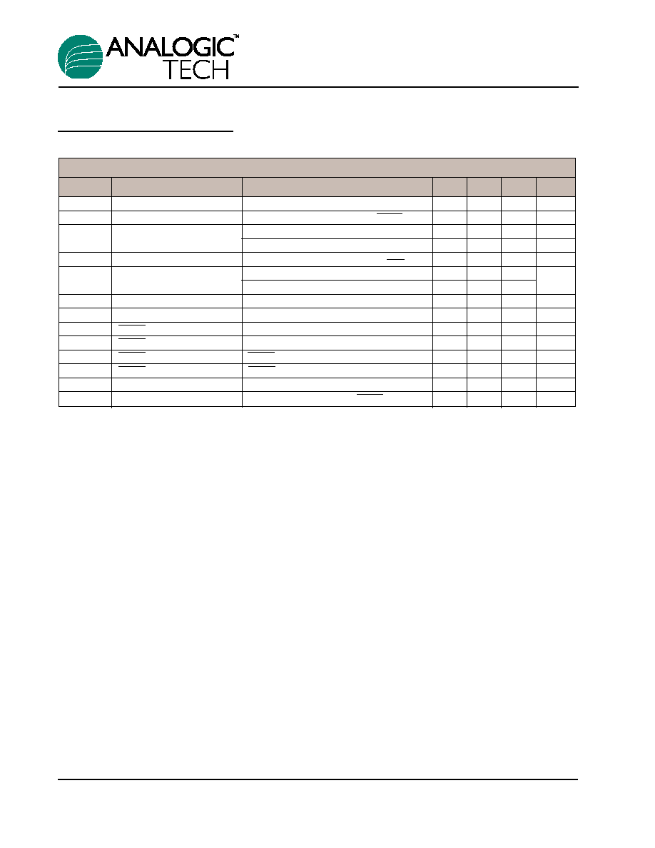
Pin #
SOT-23-6
SC70JW-8
Symbol
Function
1
1
V
OUT
Regulated output pin. Bypass this pin to ground with at
least 6.8µF low ESR capacitor
2
2, 3, 4
GND
Ground connection
3
5
SHDN
Shutdown input. Active low signal disables the converter.
4
6
C-
Flying capacitor negative terminal
5
7
V
IN
Input supply pin. Bypass this pin to ground with at least
6.8µF low ESR capacitor
6
8
C+
Flying capacitor positive terminal
AAT3111
MicroPowerTM Regulated Charge Pump
2
3111.2002.3.0.91

AAT3111
MicroPowerTM Regulated Charge Pump
3111.2002.3.0.91
3
Absolute Maximum Ratings
(T
A
=25∞C unless otherwise noted)
Stresses above those listed in Absolute Maximum Ratings may cause permanent damage to the device. Functional operation at condi-
tions other than the operating conditions specified is not implied. Only one Absolute Maximum rating should be applied at any one time.
Note 1: Human body model is a 100pF capacitor discharged through a 1.5k
resistor into each pin.
Thermal Information
Note 2: Mounted on an FR4 board.
Electrical Characteristics
(T
A
= -40 to 85∞C unless otherwise noted. Typical values are at T
A
=25∞C,
C
FLY
=1µF, C
IN
=10µF, C
OUT
=10µF)
Note 3: I
Q
= I
VIN
+ I
VOUT
. V
OUT
is pulled up to 3.8V to prevent switching.
AAT3111-3.3
Symbol
Description
Conditions
Min
Typ
Max
Units
V
IN
Input Voltage
V
OUT
=3.3V
1.8
V
OUT
V
I
Q
No Load Supply Current
3
1.8V < V
IN
< 3.3V, I
OUT
=0mA, SHDN = V
IN
20
30
µA
V
OUT
Output Voltage
1.8V < V
IN
< 3.3V, I
OUT
=20mA
3.17
3.30
3.43
V
2.5V < V
IN
< 3.3V, I
OUT
=100mA
3.17
3.30
3.43
V
I
SHDN
Shutdown Supply Current
1.8V < V
IN
< 3.3V, I
OUT
=0mA, V
SHDN
=0
0.01
1
µA
V
RIPPLE
Ripple Voltage
V
IN
= 2.0V, I
OUT
= 50mA
20
mV
P-P
Efficiency
V
IN
= 1.8V, I
OUT
= 25mA
91
%
f
OSC
Frequency
Oscillator Free Running
750
kHz
V
IH
SHDN Input Threshold High
1.4
V
V
IL
SHDN Input Threshold Low
0.3
V
I
IH
SHDN Input Current High
SHDN = V
IN
-1
1
µA
I
IL
SHDN Input Current Low
SHDN = GND
-1
1
µA
t
ON
V
OUT
Turn-on time
V
IN
= 1.8V, I
OUT
= 0mA
0.2
ms
I
SC
Short-circuit current
4
V
IN
= 1.8V, V
OUT
= GND, SHDN = 3V
300
mA
Symbol
Description
Rating
Units
JA
Maximum Thermal Resistance (SOT23-6 or SC70JW-8)
150
∞C/W
P
D
Maximum Power Dissipation (SOT23-6 or SC70JW-8)
667
mW
Symbol
Description
Value
Units
V
IN
V
IN
to GND
-0.3 to 6
V
V
OUT
V
OUT
to GND
-0.3 to 6
V
V
SHDN
SHDN to GND
-0.3 to 6
V
t
SC
Output to GND Short-Circuit Duration
Indefinite
s
T
J
Operating Junction Temperature Range
-40 to 150
∞C
T
LEAD
Maximum Soldering Temperature (at leads, 10 sec)
300
∞C
V
ESD
ESD Rating
1
-- HBM
2000
V
Electrical Characteristics
(T
A
= -40 to 85∞C unless otherwise noted. Typical values are at T
A
=25∞C,
C
FLY
=1µF, C
IN
=10µF, C
OUT
=10µF)
Note 4: Under short-circuit conditions, the device may enter overtemperature protection mode.
Note 5: I
Q
= I
VIN
+ I
VOUT
. V
OUT
is pulled up to 4.1V to prevent switching.
AAT3111-3.6
Symbol
Description
Conditions
Min
Typ
Max
Units
V
IN
Input Voltage
V
OUT
=3.6V
1.8
V
OUT
V
I
Q
No Load Supply Current
5
1.8V < V
IN
< 3.6V, I
OUT
=0mA, SHDN=V
IN
20
30
µA
V
OUT
Output Voltage
2.0V < V
IN
< 3.6V, I
OUT
20mA
3.46
3.6
3.74
V
3.0V < V
IN
< 3.6V, I
OUT
100mA
3.46
3.6
3.74
V
I
SHDN
Shutdown Supply Current
1.8V < V
IN
< 3.6V, I
OUT
=0mA, V
SHDN
=0
0.01
1
µA
V
RIPPLE
Ripple Voltage
V
IN
= 2.5V, I
OUT
= 50mA
25
mV
P-P
V
IN
= 3V, I
OUT
= 100mA
30
Efficiency
V
IN
= 2.0V, I
OUT
= 20mA
90
%
f
OSC
Frequency
Oscillator Free Running
750
kHz
V
IH
SHDN Input Threshold High
1.4
V
V
IL
SHDN Input Threshold Low
0.3
V
I
IH
SHDN Input Current High
SHDN = V
IN
-1
1
µA
I
IL
SHDN Input Current Low
SHDN = GND
-1
1
µA
t
ON
V
OUT
Turn-on time
V
IN
= 1.8V, I
OUT
= 0mA
0.2
ms
I
SC
Short-circuit current
4
V
IN
= 1.8V, V
OUT
= GND, SHDN = 3V
300
mA
AAT3111
MicroPowerTM Regulated Charge Pump
4
3111.2002.3.0.91

AAT3111
MicroPowerTM Regulated Charge Pump
3111.2002.3.0.91
5
Typical Characteristics -- AAT3111-3.3
(Unless otherwise noted, V
IN
= 3V, C
IN
= C
OUT
=10µF, C
FLY
= 1µF, T
A
= 25∞C)
V
SHDN
Threshold vs. Supply Voltage
0.4
0.5
0.6
0.7
0.8
0.9
1.5
1.7
1.9
2.1
2.3
2.5
2.7
2.9
3.1
Supply Voltage (V)
V
SHDN
Threshold (V)
V
IH
V
IL
Startup
Time (100
µ
s/div.)
SHDN (2V/div)
V
OUT
(1V/div)
I
LOAD
=100mA
V
IN
=2.3V
I
LOAD
=25mA
V
IN
=2.0V
I
LOAD
=50mA
V
IN
=2.0V
Efficiency vs. Load Current
0%
10%
20%
30%
40%
50%
60%
70%
80%
90%
100%
0.01
0.1
1
10
100
Load Current (mA)
Efficiency (%)
V
IN
=1.8V
V
IN
=2.0V
V
IN
=2.6V
Efficiency vs. Supply Voltage
50%
55%
60%
65%
70%
75%
80%
85%
90%
95%
1.8
2.0
2.2
2.4
2.6
2.8
3.0
Supply Voltage (V)
Efficiency (%)
100mA
5mA
50mA
Supply Current vs. Supply Voltage
0
10
20
30
40
50
60
1.5
2.0
2.5
3.0
3.5
Supply Voltage (V)
Supply Current (
µ
A)
No Load, Switching
No Load, Not Switching
Output Voltage vs. Output Current
3.20
3.25
3.30
3.35
3.40
0.01
0.1
1
10
100
1000
Output Current (mA)
Output Voltage (V)
V
IN
=1.7V
V
IN
=2.3V
V
IN
=2.6V
V
IN
=2.0V