
AAT3113/4
High Efficiency 1.5X Fractional Charge
Pumps For White LED Applications
Typical Application
C
IN
1
µ
F
V
BATTERY
C
OUT
1
µ
F
EN/SET
C1
1
µ
F
C2
1
µ
F
D4
D3
D2
D1
V
IN
V
OUT
C1+
C1-
C2+
C2-
D1
D2
D3
D4
EN/SET
GND
AAT3114
D5
D6
D5
D6
3113.2004.07.1.4
1
ChargePump
TM
General Description
The AAT3113/4 are low noise, constant frequency
charge pump DC/DC converters that use fractional
(1.5X) conversion to increase efficiency in White
LED applications. The devices can be used to pro-
duce current levels up to 20mA for each output from
a 2.7V to 5.5V input. Low external parts counts (two
1µF flying capacitors and two small bypass capaci-
tors at V
IN
, and OUT) make the AAT3113/4 ideally
suited for small battery-power applications.
AnalogicTechTM's Simple Serial ControlTM
(S
2
CwireTM) interface is used to enable, disable
and set the LED drive current for a 32 level loga-
rithmic scale LED brightness control. The
AAT3113/4 have a thermal management system to
protect the device in the event of a short circuit
condition on any of the output pins. Built-in soft-
start circuitry prevents excessive inrush current
during start-up. High switching frequency enables
the use of small external capacitors. A low current
shutdown feature disconnects the load from V
IN
and reduces quiescent current to less than 1µA.
The AAT3113 provides 4 LED current source out-
puts, and the AAT3114 provides 6. The AAT3113/4
are available in 16-pin quad QFN packages, and
the AAT3113 is also available in the 12-pin
TSOPJW package.
Features
∑
White LED Backlighting
∑
AAT3113 - 4 Outputs
∑
AAT3114 - 6 Outputs
∑
20mA Full Scale Current
∑
32 Position Logarithmic Scale with Digital
Control
∑
Simple Serial ControlTM (S
2
CwireTM) interface
∑
Low Noise Constant Frequency Operation
∑
33% Less Input Current Than Doubler
Charge Pump
∑
High Accuracy Brightness Matching
∑
Small Application Circuit
∑
Regulated Output Current
∑
Automatic Soft-Start
∑
VIN Range: 2.7V to 5.5V
∑
No Inductors
∑
600kHz Switching Frequency
∑
Iq < 1µA in Shutdown
∑
Temperature Range -40 to 85∞C.
∑
16-Pin QFN, 12-Pin TSOPJW Package
Applications
∑
White LED Backlighting
∑
Programmable Current Source

Pin Descriptions
Part Number Descriptions
Pin Configuration
12-Lead TSOPJW
16 LD 4x4mm QFN
(Top View)
(Top View)
1
2
3
4
12
11
10
9
5
6
7
8
16
15
14
13
D2
D3
D4
(D5)
(D6)
C1+
C1-
NC
OUT
C2+
C2-
GND
AAT3113/4
NC
VIN
EN/SET
D1
1
2
3
4
5
6
12
11
10
9
8
7
C2+
OUT
C1-
C1+
D
D
C2-
GND
VIN
EN/SET
D
D
Part Number
Function
AAT3113-20
4 Diode outputs, 20mA full scale
AAT3114-20
6 Diode outputs, 20mA full scale
Pin #
QFN44-16
TSOPJW-12
Symbol
Function
1
7
D2
Current source output
2
6
D3
Current source output
3
5
D4
Current source output
4
N/A
D5
Current source output (3114 option only)
5
N/A
D6
Current source output (3114 option only)
6
4
C1+
Flying Capacitor 1 + terminal
7
3
C1-
Flying Capacitor 1 - terminal
8
N/A
NC
No Connect
9
2
OUT
Charge pump output. Requires 1uF bypass capacitor to ground.
10
1
C2+
Flying Capacitor 2 + terminal
11
12
C2-
Flying Capacitor 2 - terminal
12
11
GND
Ground
13
N/A
NC
No Connect
14
10
VIN
Input power supply. Requires 1uF bypass capacitor to ground.
15
9
EN/SET
Control Pin using S
2
Cwire serial interface.
16
8
D1
Current source output 1. Required reference current source.
AAT3113/4
High Efficiency 1.5X Fractional Charge
Pumps For White LED Applications
2
3113.2004.07.1.4

Absolute Maximum Ratings
(T
A
=25∞C unless otherwise noted)
Electrical Characteristics
V
IN
=3.5V, T
A
= -40 to 85∞C unless otherwise noted. Typical values are at T
A
= 25∞C.
Symbol
Description
Conditions
Min
Typ Max Units
Input Power Supply
V
IN
Operation Range
2.7
5.5
V
I
CC
Operating Current
Active, No Load Current
1
2
mA
I
SHDN
Shutdown Current
EN=0
1
µA
IDX
Output Current
3113: 3.0
V
IN
5.5 T
A
= 25∞C, All
18
20
22
mA
3114: 3.2
V
IN
5.5 Outputs Max Current
I
D
/
V
IN
Output Current Line
3.0
V
IN
5.5
-2
2
%/V
Regulation
I(D-Match)
Current Matching between VD1:Dn=3.6, V
IN
=3.3V
0.3
%
any two outputs
Efficiency
V
IN
=3.5, I
OUT(total)
=40mA
93
%
Charge Pump
t
SS
Soft start time
400
µs
F
CLK
Clock Frequency
300
600
900
KHz
EN/SET
V
EN(L)
Enable Threshold Low
V
IN
= 2.7 to 5.5V
0.5
V
V
EN(H)
Enable Threshold High
V
IN
= 2.7 to 5.5V
1.4
V
t
LO
EN/SET low time
0.3
75
µs
t
HI
Minimum EN/SET high time
50
ns
t
OFF
EN/SET Off Timeout
300
500
µs
Input Current EN/SET input leakage
V
IN
= 5.5V
-1
1
µA
Symbol
Description
Value
Units
V
IN
Input Voltage
-0.3 to 6
V
V
OUT
Charge Pump Output
-0.3 to 6
V
V
EN/SET
EN/SET to GND Voltage
-0.3 to 6
V
V
EN/SET(MAX)
Maximum EN/SET to Input Voltage
0.3
V
I
OUT
Maximum DC Output Current (Sum of Iout and D currents)
150
mA
JA
Thermal Resistance
37
∞C/W
T
J
Operating Junction Temperature Range
-40 to 150
∞C
AAT3113/4
High Efficiency 1.5X Fractional Charge
Pumps For White LED Applications
3113.2004.07.1.4
3
Typical Characteristics
(unless otherwise noted: V
IN
=3.5V, C
IN
=C
OUT
=C1=C2=1µF, T
A
=25∞C)
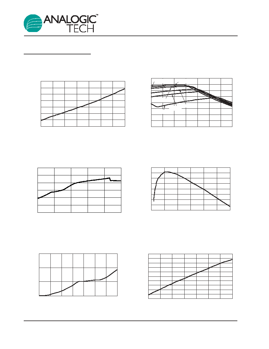
Oscillator Frequency vs. Temperature
610
620
630
640
650
660
670
680
690
700
710
-40
-20
0
20
40
60
80
100
Temperature (
∞
C)
F
OSC
(kHz)
Shutdown Current vs. Temperature
0.001
0.010
0.100
1.000
-40
-20
0
20
40
60
80
100
Temperature (
∞
C)
Shutdown Current (
µ
A)
Efficiency vs. Load Current
80%
82%
84%
86%
88%
90%
92%
94%
96%
0
20
40
60
80
100
120
Load Current (mA)
Efficiency (%)
Quiescent Current vs. Supply Voltage
0.6
0.7
0.8
0.9
1.0
1.1
1.2
3.0
3.5
4.0
4.5
5.0
5.5
Supply Voltage (V)
I
Q
(mA)
Efficiency vs. Supply Voltage
60%
65%
70%
75%
80%
85%
90%
95%
100%
3.0
3.2
3.4
3.6
3.8
4.0
4.2
4.4
Supply Voltage (V)
Efficiency
120 mA
80 mA
60 mA
40 mA
30 mA
20 mA
Quiescent Current vs. Temperature
0.860
0.880
0.900
0.920
0.940
0.960
0.980
1.000
-40
-20
0
20
40
60
80
100
Temperature (
∞
C)
I
Q
(mA)
AAT3113/4
High Efficiency 1.5X Fractional Charge
Pumps For White LED Applications
4
3113.2004.07.1.4

Typical Characteristics
(unless otherwise noted: V
IN
=3.5V, C
IN
=C
OUT
=C1=C2=1µF, T
A
=25∞C)
V
IH
and V
IL
vs. VIN
0.750
0.775
0.800
0.825
0.850
0.875
0.900
0.925
0.950
0.975
1.000
2.5
3.0
3.5
4.0
4.5
5.0
5.5
VIN (V)
V
IH
and V
IL
(V)
V
IH
V
IL
I
DIODE
vs. V
DIODE
0
20
40
60
80
100
120
140
3.0
3.2
3.4
3.6
3.8
4.0
V
DIODE
(V)
I
DIODE
(mA)
I
DIODE
Response
-9dB to -10dB
10
µ
s/div
ENSET
(2V/div)
I
DIODE
-9 dB
0 dB
-10 dB
-31 dB
I
DIODE
vs. VIN
0
20
40
60
80
100
120
140
3.0
3.5
4.0
4.5
V
IN
(V)
I
DIODE
(mA)
I
DIODE
Response
-31dB to 0dB
10
µ
s/div
ENSET
(2V/div)
I
DIODE
-31 dB
0 dB
Normalized I
DIODE
vs. Temperature
0.950
0.960
0.970
0.980
0.990
1.000
1.010
1.020
-40
-20
0
20
40
60
80
100
Temperature (
∞
C)
I
DIODE
AAT3113/4
High Efficiency 1.5X Fractional Charge
Pumps For White LED Applications
3113.2004.07.1.4
5