AAT3132/32A
High Efficiency 1.5X Fractional Charge
Pump for White LED Applications
3132.2005.12.1.4
1
ChargePump
TM
General Description
The AAT3132/32A is a low noise, constant frequen-
cy charge pump DC/DC converter that uses frac-
tional (1.5X) conversion to maximize efficiency for
white LED applications. The device can be used to
produce current levels up to 20mA in three of its out-
puts and up to 25 or 30mA in one of its outputs to
drive LEDs from a 2.7V to 5.5V input. Outputs may
be operated individually or paralleled for driving
higher-current LEDs. A low external parts count
(two 1µF flying capacitors and two small 1µF capac-
itors at V
IN
and OUT) makes the AAT3132/32A ide-
ally suited for small battery-powered applications.
AnalogicTech's Simple Serial ControlTM (S
2
CwireTM)
interface is used to enable, disable, and set the LED
drive current in two groups: the three 20mA outputs
and the single 30mA output with multiple level loga-
rithmic scales. The AAT3132/32A has a thermal
management system to protect the device in the
event of a short-circuit condition at the output pin.
Built-in soft-start circuitry prevents excessive inrush
current during start-up. A high charge pump switch-
ing frequency enables the use of very small external
capacitors. A low-current shutdown feature discon-
nects the load from V
IN
and reduces quiescent cur-
rent to less than 1µA. The device also integrates a
test current/auto-disable feature for each channel.
The AAT3132/32A is available in the very small, Pb-
free, 12-pin TSOPJW package.
Features
∑
V
IN
Range: 2.7V to 5.5V
∑
<1.0µA of Shutdown Current
∑
1MHz Switching Frequency
∑
White LED Backlighting
∑
Fully Independent Display Lighting
∑
Drives Low-V
F
and High-V
F
Type LEDs
∑
Up to Three 20mA Outputs
∑
Single 25mA Output (AAT3132-1)
∑
Single 30mA Output (AAT3132/32A)
∑
Multi-Position Logarithmic Scale with Digital
Control
∑
Low Noise Constant Frequency Operation
∑
Regulated Output Current
∑
Automatic Soft Start
∑
No Inductors
∑
-40∞C to +85∞C Temperature Range
∑
12-Pin TSOPJW Package
Applications
∑
Color (RGB) Lighting
∑
Programmable Current Source
∑
White LED Backlighting
∑
White Photo Flash for Digital Still Cameras
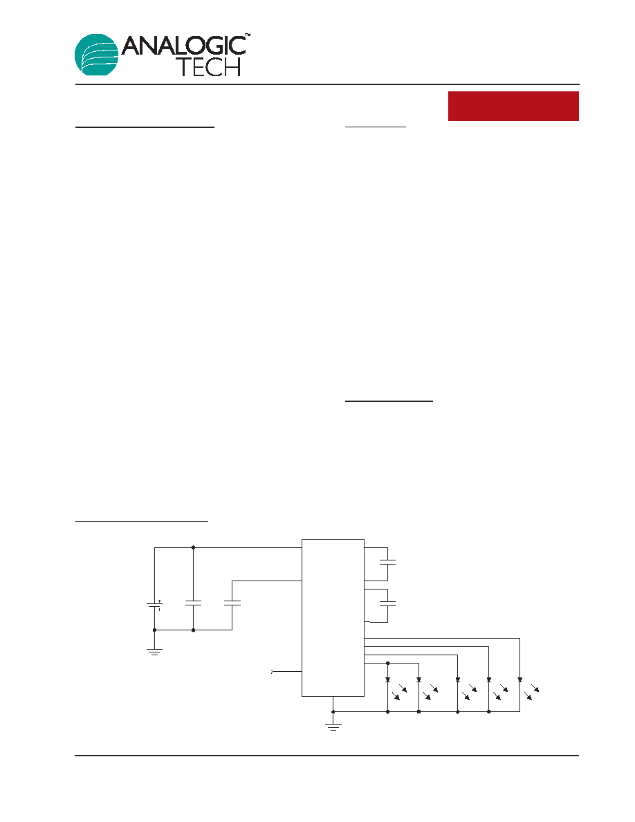
Typical Application
C
IN
1
µF
V
BATTERY
C
OUT
1
µF
EN/SET
C1
1
µF
C2
1
µF
D5
D3
D2
D1
VIN
VOUT
C1+
C1-
C2+
C2-
D1
D2
D3
D4
EN/SET
GND
AAT3132
D4
Pin Descriptions
Pin Configuration
TSOPJW-12
(Top View)
1
2
3
4
5
6
12
11
10
9
8
7
C2+
OUT
C1-
C1+
D3
D2
C2-
GND
IN
EN/SET
D1
D4
Pin #
Symbol
Function
1
C2+
Flying capacitor 2 positive terminal. Connect a 1µF capacitor between C2+
and C2-.
2
OUT
Charge pump output. Requires 1µF capacitor connected between this pin and
ground.
3
C1-
Flying capacitor 1 negative terminal.
4
C1+
Flying capacitor 1 positive terminal. Connect a 1µF capacitor between C1+
and C1-.
5
D3
Current source output #3.
6
D2
Current source output #2.
7
D4
Current source output #4.
8
D1
Current source output #1.
9
EN/SET
Control pin.
10
IN
Input power supply. Requires 1µF capacitor connected between this pin and
ground.
11
GND
Ground.
12
C2-
Flying capacitor 2 negative terminal.
AAT3132/32A
High Efficiency 1.5X Fractional Charge
Pump for White LED Applications
2
3132.2005.12.1.4
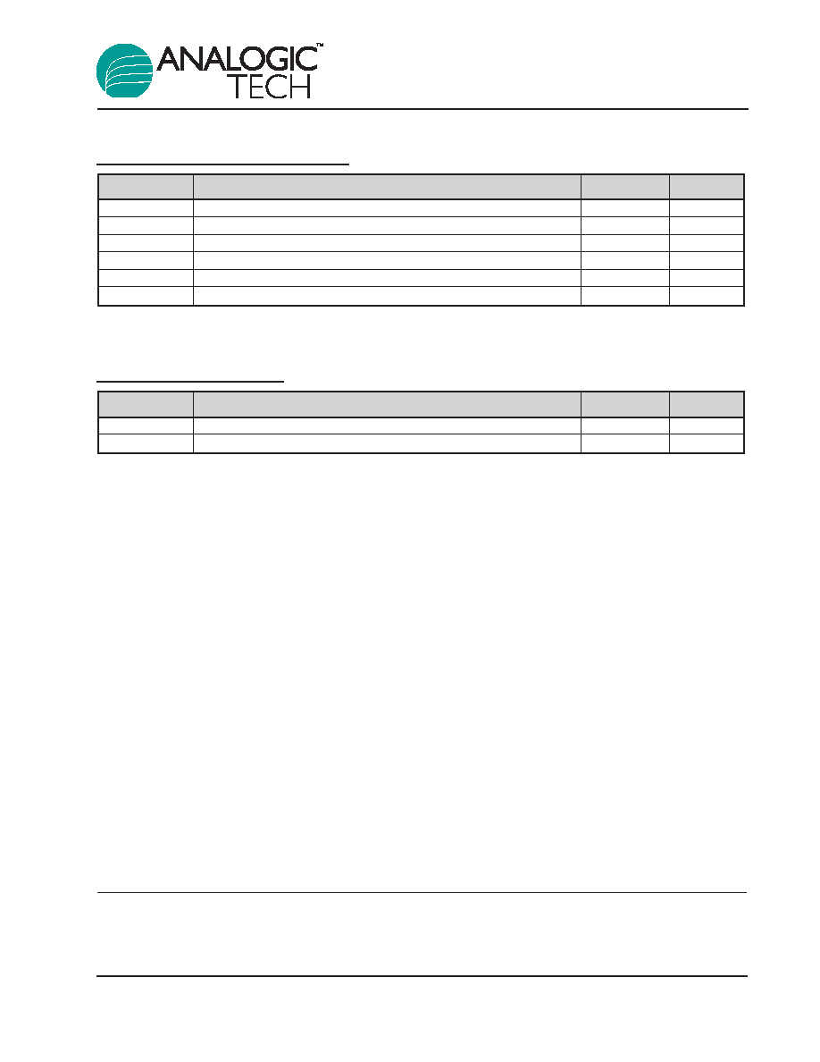
Absolute Maximum Ratings
1
Thermal Information
3
Symbol
Description
Value
Units
JA
Thermal Resistance
160
∞C/W
P
D
Maximum Power Dissipation (T
A
= 25∞C)
4
625
mW
Symbol
Description
Value
Units
V
IN
Input Voltage
-0.3 to 6
V
V
OUT
Charge Pump Output
-0.3 to 6
V
V
EN/SET
EN/SET to GND Voltage
-0.3 to 6
V
V
EN/SET(MAX)
Maximum EN/SET to Input Voltage
V
IN
- 0.3
V
I
OUT
2
Maximum DC Output Current
150
mA
T
J
Operating Junction Temperature Range
-40 to 150
∞C
AAT3132/32A
High Efficiency 1.5X Fractional Charge
Pump for White LED Applications
3132.2005.12.1.4
3
1. Stresses above those listed in Absolute Maximum Ratings may cause permanent damage to the device. Functional operation at condi-
tions other than the operating conditions specified is not implied. Only one Absolute Maximum Rating should be applied at any one time.
2. Based on long-term current density limitation.
3. Mounted on an FR4 board.
4. Derate 6.25mW/∞C above 25∞C.
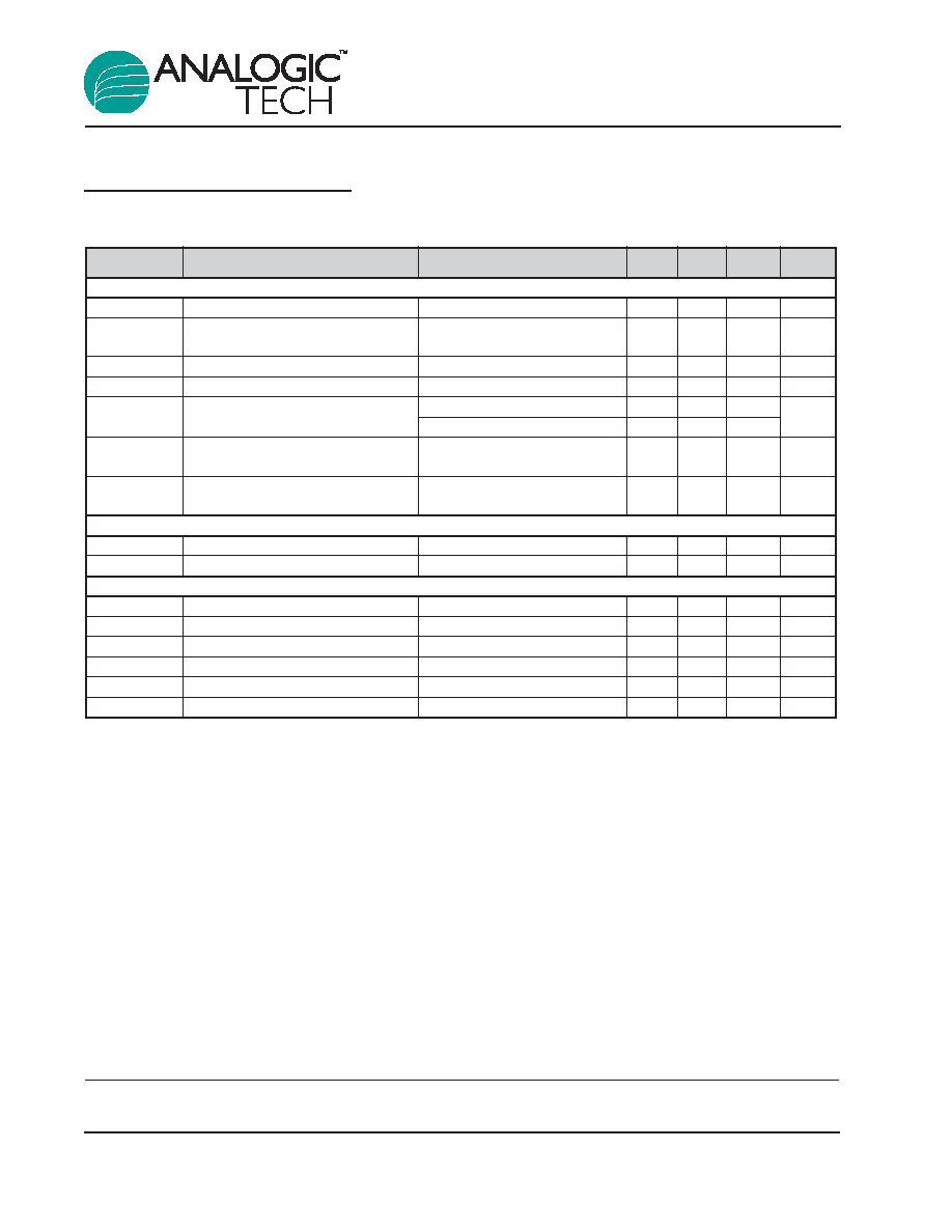
Electrical Characteristics
1
V
IN
= 3.5V, C
IN
= C
OUT
= C
1
= C
2
= 1.0µF; T
A
= -40∞C to +85∞C, unless otherwise noted.
Typical values are T
A
= 25∞C.
Symbol
Description
Conditions
Min
Typ
Max
Units
Input Power Supply
V
IN
Operation Range
2.7
5.5
V
I
CC
Operating Current
3.0
V
IN
5.5, Active,
1.8
3.5
mA
No Load Current
I
SHDN
Shutdown Current
EN = 0
1.0
µA
I
DX
Maximum Output Current D1 to D3
3.0
V
IN
5.5
18
20
22
mA
I
DX
Maximum Output Current D4
T
A
= 25∞C AAT3132-1
22.5
25
27.5
mA
T
A
= 25∞C AAT3132
27
30
33
I
(D-Match)
Current Matching Between
VD1:D3 = 3.6, V
IN
= 3.3V
0.5
%
Any Two Outputs
CP
Charge Pump Section Efficiency
V
IN
= 3.5V, I
OUT(TOTAL)
= 90mA,
93
%
Measured from IN to OUT
Charge Pump Section
T
SS
Soft-Start Time
200
µs
F
CLK
Clock Frequency
1000
kHz
EN/SET
V
EN(L)
Enable Threshold Low
0.5
V
V
EN(H)
Enable Threshold High
1.4
V
T
EN/SET LO
EN/SET Low Time
V
EN/SET
< 0.5
0.3
75
µs
T
EN/SET HI
Minimum EN/SET High Time
V
EN/SET
> 1.4
50
ns
T
OFF
EN/SET Off Timeout
V
EN/SET
< 0.5
500
µs
Input Current EN/SET Input Leakage
-1
1
µA
AAT3132/32A
High Efficiency 1.5X Fractional Charge
Pump for White LED Applications
4
3132.2005.12.1.4
1. The AAT3132/32A is guaranteed to meet performance specifications over the -40∞C to +85∞C operating temperature range and is
assured by design, characterization, and correlation with statistical process controls.
AAT3132/32A
High Efficiency 1.5X Fractional Charge
Pump for White LED Applications
3132.2005.12.1.4
5
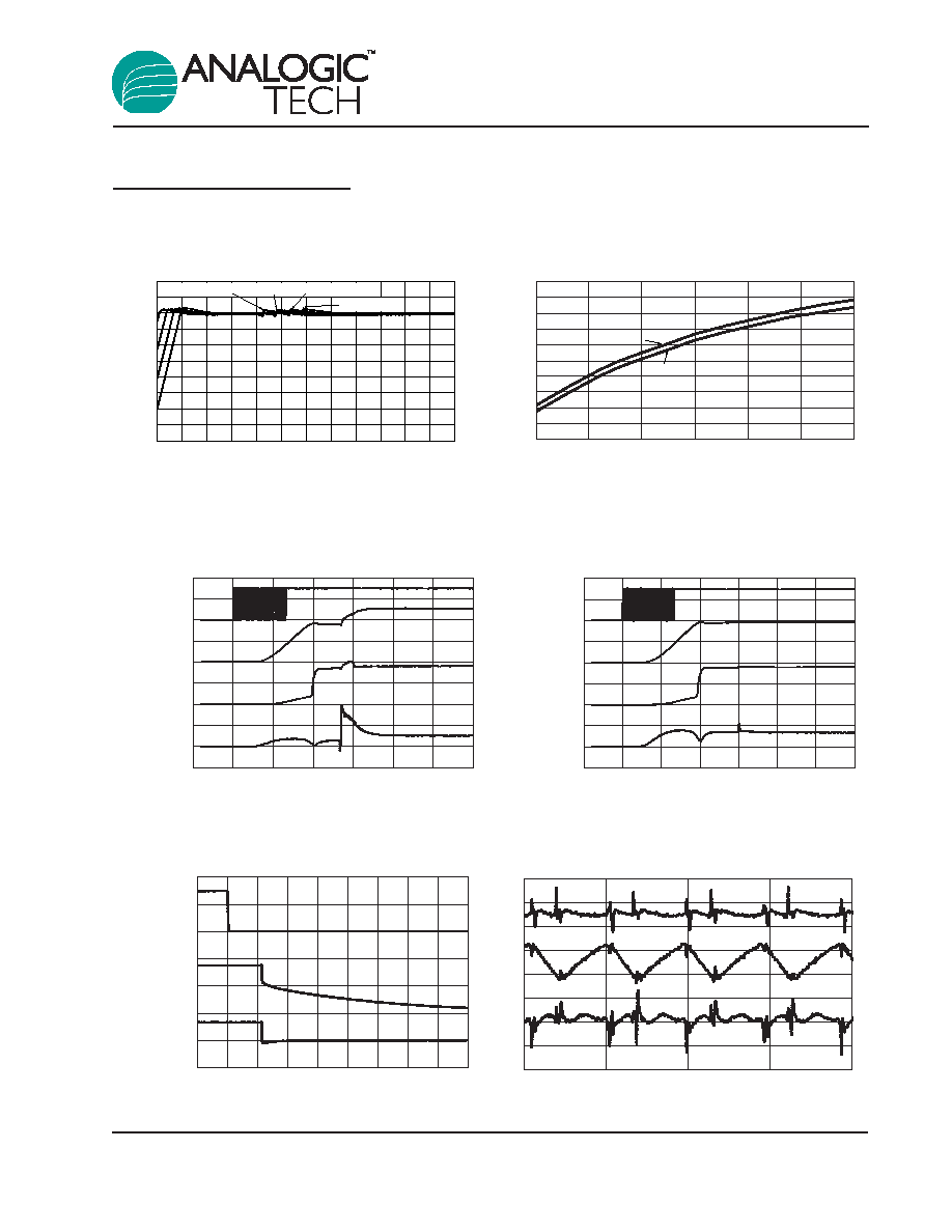
Typical Characteristics
Unless otherwise noted, V
IN
= 3.5V, C
IN
= C
OUT
= C
1
= C
2
= 1µF, T
A
= 25∞C.
80mA Load Characteristics
Time (1µs/div)
20mV/div
V
IN
OUT
V
DIODE
Turn-Off
Time (200µs/div)
ENSET
(1V/div)
V
DIODE
(2V/div)
I
IN
(100mA/div)
Turn-On to Full-Scale Load Switch
Time (50µs/div)
ENSET
(1V/div)
OUT
(2V/div)
V
DIODE
(2V/div)
I
IN
(100mA/div)
Turn-On to Full-Scale Charge Pump
Time (50µs/div)
ENSET
(1V/div)
OUT
(2V/div)
V
DIODE
(1V/div)
I
IN
(200mA/div)
V
IH
and V
IL
vs. V
IN
0.600
0.625
0.650
0.675
0.700
0.725
0.750
0.775
0.800
0.825
0.850
2.5
3.0
3.5
4.0
4.5
5.0
5.5
Input Voltage (V)
V
IH
V
IL
I
DIODE
vs. Input Voltage
(4x20mA)
40
45
50
55
60
65
70
75
80
85
90
2.7 2.9
3.1 3.3
3.5
3.7
3.9
4.1 4.3
4.5
4.7 4.9
5.1
Input Voltage (V)
I
DIODE
(mA)
V
DIODE
= 3.3V
V
DIODE
= 3.4V V
DIODE
= 3.5V
V
DIODE
= 3.6V