AAT3221/2
150mA NanoPowerTM LDO Linear Regulator
Preliminary
Information
3221.2002.03.0.94
1
PowerLinear
TM
General Description
The AAT3221 and AAT3222 PowerLinearTM
NanoPower Low Dropout Linear Regulators are
ideal for portable applications where extended bat-
tery life is critical. This device features extremely
low quiescent current which is typically 1.1µA.
Dropout voltage is also very low, typically less than
200mV at the maximum output current of 150mA.
The AAT3221/2 has an Enable pin feature, which
when asserted will enter the LDO regulator into a
shutdown mode removing power from its load and
offering extended power conservation capabilities
for portable battery powered applications.
The AAT3221/2 has output short circuit and over
current protection. In addition, the device also has
an over temperature protection circuit, which will
shutdown the LDO regulator during extended over-
current events. It is available with active high or
active low enable input.
The AAT3221 and AAT3222 are available in space
saving 5-pin SOT23 packages. The AAT3221 is
also available in the 8-pin SC70JW package. The
device is rated over a -40∞C to 85∞C temperature
range. Since only a small, 1µF ceramic output
capacitor is recommended, often the only space
used is that occupied by the AAT3221/2 itself. The
AAT3221/2 is truly a compact and cost effective volt-
age conversion solution.
The AAT3221/2 is similar to the AAT3220 with the
exception that it offers further power savings with
its enable pin.
Features
∑
1.1 µA Quiescent Current
∑
Low Dropout: 200 mV (typical)
∑
Guaranteed 150 mA Output
∑
High accuracy: ±2%
∑
Current limit protection
∑
Over-Temperature protection
∑
Extremely Low power shutdown mode
∑
Low Temperature Coefficient
∑
Factory programmed output voltages
∑
1.8V to 3.5V
∑
Stable operation with virtually any output
capacitor type
∑
Active high or low Enable pin
∑
5-pin SOT23 or 8-pin SC70JW packages
∑
4kV ESD
Applications
∑
Cellular Phones
∑
Notebook Computers
∑
Portable Communication Devices
∑
Handheld Electronics
∑
Remote Controls
∑
Digital Cameras
∑
PDAs
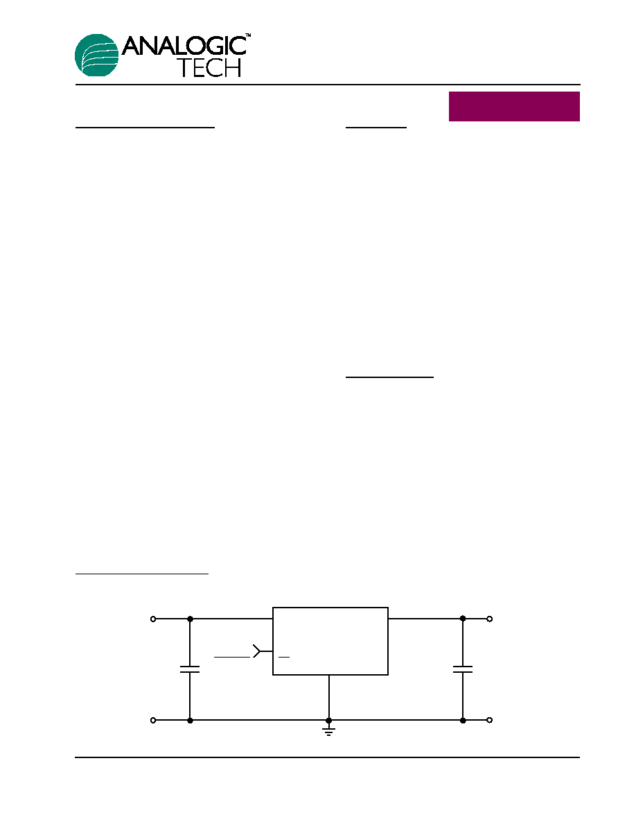
Typical Application
AAT3221/2
IN
EN
INPUT
GND
OUT
OUTPUT
GND
GND
ENABLE
(ENABLE)
C
IN
1
µ
F
C
OUT
1
µ
F
(EN)

Pin Descriptions
Pin Configuration
AAT3221
AAT3221
AAT3222
SOT23-5
SC70JW-8
SOT23-5
(Top View)
(Top View)
(Top View)
1
2
3
NC
OUT
EN (EN)
IN
4
5
GND
IN
NC
(EN) EN
1
2
GND
GND
GND
GND
OUT
1
2
3
4
8
7
6
5
1
2
3
NC
OUT
(EN) EN
4
5
IN
GND
Pin #
AAT3221
AAT3222
SOT23-5
SC70JW-8
Symbol
Function
1
2
2
IN
Input pin
2
5, 6, 7, 8
1
GND
Ground connection pin
3
4
5
EN (EN)
Enable Input. Logic compatible enable with
active high or active low option available; see
Ordering Information and Applications
Information for details.
4
3
4
NC
Not Connected
5
1
3
OUT
Output pin - should be decoupled with 1µF or
greater capacitor
AAT3221/2
150mA NanoPowerTM LDO Linear Regulator
2
3221.2002.03.0.94
Absolute Maximum Ratings
(T
A
=25∞C unless otherwise noted)
Note: Stresses above those listed in Absolute Maximum Ratings may cause permanent damage to the device. Functional operation at con-
ditions other than the operating conditions specified is not implied. Only one Absolute Maximum rating should be applied at any one time.
Thermal Information
Note 1: Mounted on a demo board.
Recommended Operating Conditions
Symbol
Description
Rating
Units
V
IN
Input Voltage
(V
OUT
+0.34) to 5.5
V
T
Ambient Temperature Range
-40 to +85
∞C
Symbol
Description
Rating
Units
JA
Thermal Resistance (SOT23-5 or SC70JW-8)
1
150
∞C/W
P
D
Power Dissipation (SOT23-5 or SC70JW-8)
1
667
mW
Symbol
Description
Value
Units
V
IN
Input Voltage
-0.3 to 6
V
V
EN
EN (EN) to GND Voltage
-0.3 to 6
V
V
ENIN(MAX)
Maximum EN (EN) to Input Voltage
0.3
V
I
OUT
Maximum DC Output Current
P
D
/(V
IN
-V
O
)
mA
T
J
Operating Junction Temperature Range
-40 to 150
∞C
T
LEAD
Maximum Soldering Temperature (at leads, 10 sec)
300
∞C
AAT3221/2
150mA NanoPowerTM LDO Linear Regulator
3221.2002.03.0.94
3

AAT3221/2
150mA NanoPowerTM LDO Linear Regulator
4
3221.2002.03.0.94
Electrical Characteristics
(V
IN
=V
OUT(NOM)
+1V, I
OUT
=1mA, C
OUT
=1µF, T
A
=25∞C unless otherwise noted)
Note 1: V
DO
is defined as V
IN
- V
OUT
when V
OUT
is 98% of nominal.
Symbol
Description
Conditions
Min
Typ
Max
Units
V
OUT
DC Output Voltage Tolerance
-2.0
2.0
%
V
OUT
=2.8V
-1.4
1.4
I
OUT
Output Current
V
OUT
> 1.2 V
150
mA
I
SC
Short Circuit Current
V
OUT
< 0.4 V
350
mA
I
Q
Ground Current
V
IN
= 5 V, no load
1.1
2.5
µA
I
SD
Shutdown Current
EN = inactive
20
nA
V
OUT
/V
OUT
Line Regulation
V
IN
= 4.0-5.5 V
0.15
0.4
%/V
V
OUT
= 1.8
1.0
1.65
V
OUT
= 2.0
0.9
1.58
V
OUT
= 2.3
0.8
1.45
V
OUT
= 2.4
0.8
1.40
V
OUT
= 2.5
0.8
1.35
V
OUT
/V
OUT
Load Regulation
I
L
=1 to 100mA
V
OUT
= 2.7
0.7
1.25
%
V
OUT
= 2.8
0.7
1.20
V
OUT
= 2.85
0.7
1.20
V
OUT
= 3.0
0.6
1.15
V
OUT
= 3.3
0.5
1.00
V
OUT
= 3.5
0.5
1.00
V
OUT
= 1.8
290
340
V
OUT
= 2.0
265
315
V
OUT
= 2.3
230
275
V
OUT
= 2.4
220
265
V
OUT
= 2.5
210
255
V
DO
Dropout Voltage
1
I
OUT
= 100mA
V
OUT
= 2.7
200
240
mV
V
OUT
= 2.8
190
235
V
OUT
= 2.85
190
230
V
OUT
= 3.0
190
225
V
OUT
= 3.3
180
220
V
OUT
= 3.5
180
220
V
EN(L)
EN Input Low Voltage
0.8
V
V
EN(H)
EN Input High Voltage
V
IN
= 2.7 V to 3.6 V
2.0
V
V
IN
= 5 V
2.4
V
I
EN(SINK)
EN Input leakage
V
ON
= 5.5 V
0.01
1
µA
PSRR
Power Supply Rejection Ratio
100 Hz
50
dB
T
SD
Over Temp Shutdown Threshold
140
∞C
T
HYS
Over Temp Shutdown Hysteresis
20
∞C
e
N
Output Noise
350
µV
RMS
T
C
Output Voltage Temp. Coefficient
80
PPM/∞C
AAT3221/2
150mA NanoPower LDO Linear Regulator
3221.2002.03.0.94
5
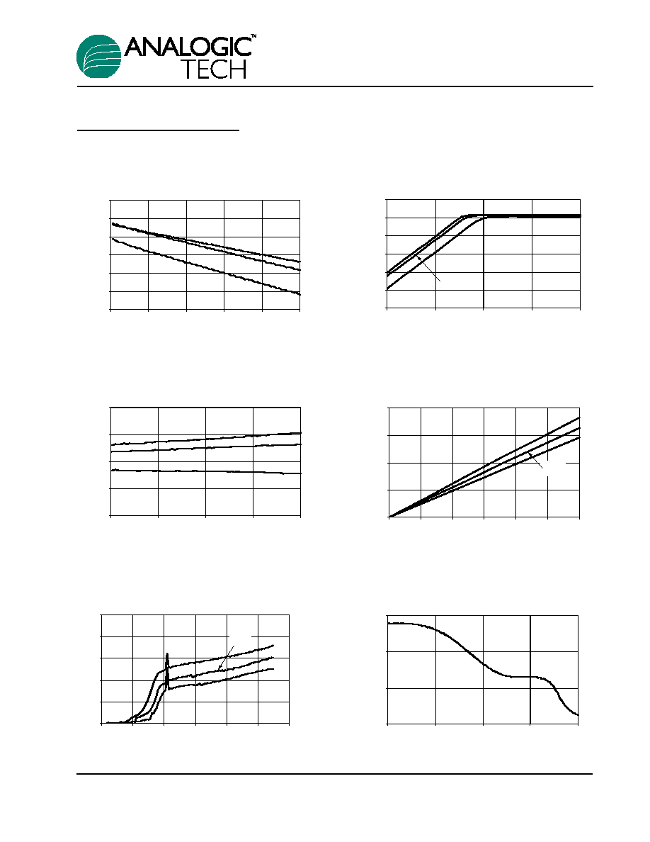
Typical Characteristics
(Unless otherwise noted, V
IN
= V
OUT
+ 1V, T
A
= 25 C, C
OUT
= 5.6 F ceramic, I
OUT
= 100mA)
PSRR with 10mA Load
0
20
40
60
1.E+01
1.E+02
1.E+03
1.E+04
1.E+05
Frequency (Hz)
PSRR
(
dB
)
Supply Current vs. Input Voltage
0
1
2
3
4
5
0
1
2
3
4
5
6
Input ( V )
Input
(
µ
A
)
with
No
Load
80
∞
C
-30
∞
C
25
∞
C
Drop-out Voltage vs. Output Current
0
100
200
300
40 0
0
25
50
75
100
125
150
Output (mA)
Drop-out
(
m
V
)
80
∞
C
-30
∞
C
25
∞
C
Output Voltage vs. Input Voltage
2.99
3
3.01
3.02
3.03
3.5
4
4.5
5
5.5
Input ( V )
O
u
tput
(
V
)
1mA
10mA
40mA
Output Voltage v. Input Voltage
2.5
2.6
2.7
2.8
2.9
3
3.1
2.7
2.9
3.1
3.3
3.5
Input (V)
O
u
tput
(
V
)
1mA
10mA
40mA
Output Voltage vs. Output Current
2.97
2.98
2.99
3
3.01
3.02
3.03
0
20
40
60
80
100
Output (mA)
O
u
tput
(
V
)
80
∞
C
25
∞
C
-30
∞
C