
AAT3223
250mA NanoPowerTM LDO
Linear Regulator with Power-OK
3223.2005.04.1.4
1
PowerLinear
TM
General Description
The AAT3223 PowerLinear NanoPower low
dropout (LDO) linear regulator is ideal for portable
applications where extended battery life is critical.
This device features extremely low quiescent cur-
rent which is typically 1.1µA. Dropout voltage is
also very low, typically 190mV at 100mA. The
AAT3223 has an enable pin feature which, when
pulled low, will put the LDO regulator into shutdown
mode, removing power from its load and offering
extended power conservation capabilities for
portable battery-powered applications. The
AAT3223 also has a Power-OK (POK) feature.
The POK function monitors the LDO output voltage
and will alert the system if the output falls out of
regulation.
The AAT3223 has output short-circuit and over-
current protection. In addition, the device has an
over-temperature protection circuit, which will shut
down the LDO regulator during extended over-cur-
rent events.
The AAT3223 is available in a space-saving 6-pin
SOT23 package and is rated over the -40∞C to
+85∞C temperature range.
The AAT3223 is similar to the AAT3221 with the
exception that it offers the additional Power-OK
function through the POK pin.
Features
∑
1.1µA Quiescent Current
∑
250mA Output Current
∑
Low Dropout: 190mV (typical)
∑
High Accuracy: ±2%
∑
Current Limit Protection
∑
Over-Temperature Protection
∑
Extremely Low Power Shutdown Mode
∑
Low Temperature Coefficient
∑
Stable Operation With Virtually Any Output
Capacitor Type
∑
Power-OK Signal Output
∑
Active High Enable Pin
∑
4kV ESD
∑
Factory-Programmed Output Voltages
∑
6-pin SOT23 Package
Applications
∑
Cellular Phones
∑
Digital Cameras
∑
Handheld Electronics
∑
Notebook Computers
∑
PDAs
∑
Portable Communication Devices
∑
Remote Controls
Typical Application
AAT3223
1
µ
F
1
µ
F
OUT
IN
POK
EN
GND
V
OUT
GND
GND
V
IN
ON/OFF
100k
POK
Pin Descriptions
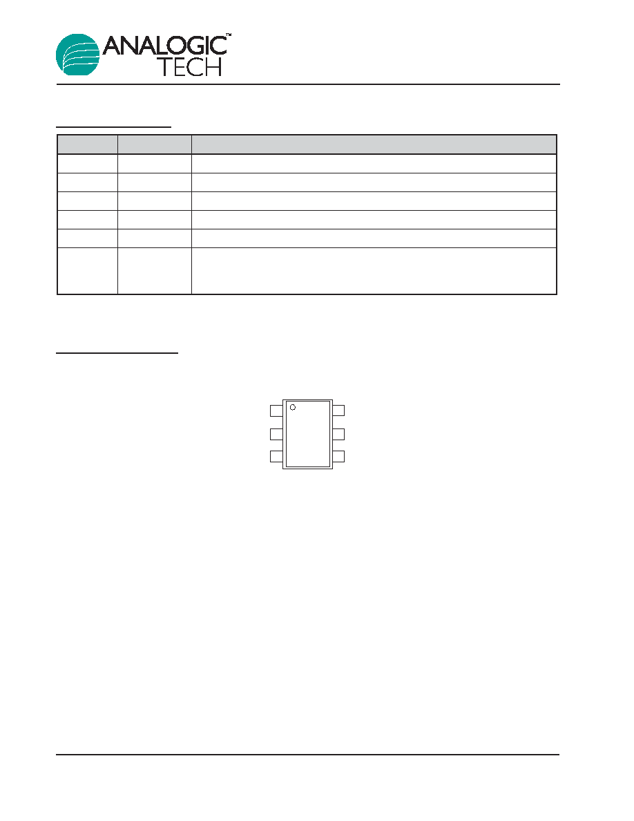
Pin Configuration
SOT23-6
(Top View)
GND
POK
EN
N/C
OUT
IN
1
2
3
4
5
6
Pin #
Symbol
Function
1
IN
Input pin. It is recommended to bypass this pin with a 1µF capacitor.
2
GND
Ground connection pin.
3
OUT
Output pin. This pin should be decoupled with a 1µF or larger capacitor.
4
N/C
Not connected.
5
EN
Enable input. Active high, logic level compatible.
6
POK
Power-OK output pin. This pin is pulled to ground during a power failure; it
is normally high impedance and should have a 100k
pull-up resistor con-
nected to OUT.
AAT3223
250mA NanoPowerTM LDO
Linear Regulator with Power-OK
2
3223.2005.04.1.4

Absolute Maximum Ratings
1
T
A
=25∞C, unless otherwise noted.
Thermal Information
2
Recommended Operating Conditions
Symbol
Description
Rating
Units
V
IN
Input Voltage
4
(V
OUT
+V
DO
) to 5.5
V
T
Ambient Temperature Range
-40 to +85
∞C
Symbol
Description
Rating
Units
JA
Thermal Resistance (SOT23-6)
150
∞C/W
P
D
Power Dissipation (SOT23-6) (T
A
= 25∞C)
3
667
mW
Symbol
Description
Value
Units
V
IN
Input Voltage
-0.3 to 6
V
V
EN
EN to GND Voltage
-0.3 to 6
V
V
ENIN(MAX)
Maximum EN to Input Voltage
0.3
V
I
OUT
Maximum DC Output Current
P
D
/(V
IN
-V
O
)
mA
T
J
Operating Junction Temperature Range
-40 to 150
∞C
T
LEAD
Maximum Soldering Temperature (at leads, 10 sec)
300
∞C
AAT3223
250mA NanoPowerTM LDO
Linear Regulator with Power-OK
3223.2005.04.1.4
3
1. Stresses above those listed in Absolute Maximum Ratings may cause permanent damage to the device. Functional operation at condi-
tions other than the operating conditions specified is not implied. Only one Absolute Maximum Rating should be applied at any one time.
2. Mounted on a demo board.
3. Derate 6.7mW/∞C above 25∞C.
4. To calculate minimum input voltage, use the following equation: V
IN(MIN)
= V
OUT(MAX)
+ V
DO(MAX)
as long as V
IN
2.5V.

Electrical Characteristics
V
IN
= V
OUT(NOM)
+ 1V, I
OUT
= 1mA, C
OUT
= 1µF, T
A
= 25∞C, unless otherwise noted.
Symbol
Description
Conditions
Min
Typ
Max
Units
V
OUT
DC Output Voltage Tolerance
-2.0
2.0
%
I
OUT
Output Current
V
OUT
> 1.2V
250
mA
I
SC
Short-Circuit Current
V
OUT
< 0.4V
400
mA
I
Q
Ground Current
V
IN
= 5V, No Load
1.1
2.5
µA
I
Q-OFF
Off-Supply Current
V
IN
= 5V, EN = Inactive
0.01
1
µA
V
OUT
/V
OUT
Line Regulation
V
IN
= 4.0V to 5.5V
0.15
0.4
%/V
V
OUT
= 1.8
1.0
1.65
V
OUT
= 2.7
0.7
1.25
V
OUT
= 2.8
0.7
1.20
V
OUT
/V
OUT
Load Regulation
I
L
=1 to 100mA
V
OUT
= 2.85
0.7
1.20
%
V
OUT
= 3.0
0.6
1.15
V
OUT
= 3.3
0.5
1.00
V
OUT
= 2.7
200
240
V
OUT
= 2.8
190
235
V
DO
Dropout Voltage
1, 2
I
OUT
= 100mA
V
OUT
= 2.85
190
230
mV
V
OUT
= 3.0
190
225
V
OUT
= 3.3
180
220
PSRR
Power Supply Rejection Ratio
100Hz
50
dB
T
SD
Over-Temperature Shutdown
140
∞C
Threshold
T
HYS
Over-Temperature Shutdown
20
∞C
Hysteresis
e
N
Output Noise
350
µV
RMS
T
C
Output Voltage Temperature
80
PPM/∞C
Coefficient
POK
POK
TH
POK Trip Threshold
Falling
25∞C
87.5
90.5
93.5
-40 to 85∞C
86
95
% of
POK
HYS
POK Hysteresis
1.5
V
OUT
I
POK
POK Off-Current
V
POK
= 5.5V, T
A
= 25∞C
100
nA
V
POK
POK Low Voltage
I
POK
= 1mA
200
mV
T
POK
POK Delay
V
OUT
Rising
1.5
ms
EN
V
IH
EN Input Threshold
V
IN
= 2.5V to 5.5V
2
V
V
IL
EN Input Threshold
V
IN
= 2.5V to 5.5V
0.5
I
EN(SINK)
EN Input Leakage
V
ON
= 5.5V
0.01
1
µA
AAT3223
250mA NanoPowerTM LDO
Linear Regulator with Power-OK
4
3223.2005.04.1.4
1. V
DO
is defined as V
IN
- V
OUT
when V
OUT
is 98% of nominal.
2. For V
OUT
< 2.3V, V
DO
= 2.5V - V
OUT
.

AAT3223
250mA NanoPowerTM LDO
Linear Regulator with Power-OK
3223.2005.04.1.4
5
Typical Characteristics
Unless otherwise noted, V
IN
= V
OUT
+ 1V, T
A
= 25∞C, C
IN
= C
OUT
= 1µF ceramic.
PSRR With 10mA Load
0
20
40
60
1.E+01
1.E+02
1.E+03
1.E+04
1.E+05
Frequency (Hz)
PSRR
(
d
B
)
Supply Current vs. Input Voltage
0.0
0.2
0.4
0.6
0.8
1.0
1.2
1.4
1.6
1.8
2.0
0
1
2
3
4
5
6
Input Voltage (V)
Input (
µ
A) with No Load
80
∞
C
25
∞
C
-30
∞
C
Dropout Voltage vs. Output Current
0
100
200
300
40 0
0
25
50
75
100
125
150
Output Current (mA)
Dropout Voltage (mV)
80∞C
-30∞C
25∞C
Output Voltage vs. Input Voltage
2.99
3
3.01
3.02
3.03
3.5
4
4.5
5
5.5
1mA
10mA
40mA
Input Voltage (V)
Output Voltage (V)
Output Voltage vs. Input Voltage
2.5
2.6
2.7
2.8
2.9
3
3.1
2.7
2.9
3.1
3.3
3.5
1mA
10mA
40mA
Input Voltage (V)
Output Voltage (V)
Output Voltage vs. Output Current
2.97
2.98
2.99
3
3.01
3.02
3.03
0
20
40
60
80
100
Output Current (mA)
Output Voltage (V)
80
∞
C
25
∞
C
-30
∞
C