AAT3232
300mA CMOS Low Drop Out Linear Regulator
Advanced Analogic Technologies, Inc.
1250 Oakmead Pkwy, Suite 310, Sunnyvale, CA 94086
(408)524-9684 Fax (408)524-9689
$1$/2*,&
7(&+
TM
3232.2000.05.0.98
General Description
The AAT3232 Low Dropout Linear Regulator is
ideal for portable applications where longer
battery life is critical. It features low quiescent
current (30
µ
A typical) and low dropout voltage
(300mV max) at full output current. The device is
able to protect itself from short circuit conditions
with fold back current limiting. Thermal shutdown
is activated to prevent damage under extreme
conditions.
The AAT3232 also features a low-power
shutdown mode for longer battery life. A pin is
provided to improve PSRR performance, by
connecting an external capacitor from the
AAT3232's reference output to ground.
The AAT3232 is available in a space saving 5-pin
SOT-23 in 7 factory programmed voltages of
2.5V, 2.7V, 2.8V, 3.0V, 3.3V, 3.5V and 3.8V.
Features
∑
Low Dropout - 300mV (max) at 300mA
∑
Guaranteed
300mA
Output
∑
High
accuracy
∑
30
µ
A Quiescent Current
∑
Current
limit
protection
∑
Short circuit current fold back
∑
Over-Temperature
protection
∑
Noise reduction bypass capacitor
∑
Shutdown mode for longer battery life
∑
Low Temperature coefficient
∑
7 Factory programmed output voltages
∑
SOT-23
5-pin
package
Applications
∑
Cellular
Phones
∑
Notebook
Computers
∑
Portable Communication Devices
∑
Handheld
Electronics
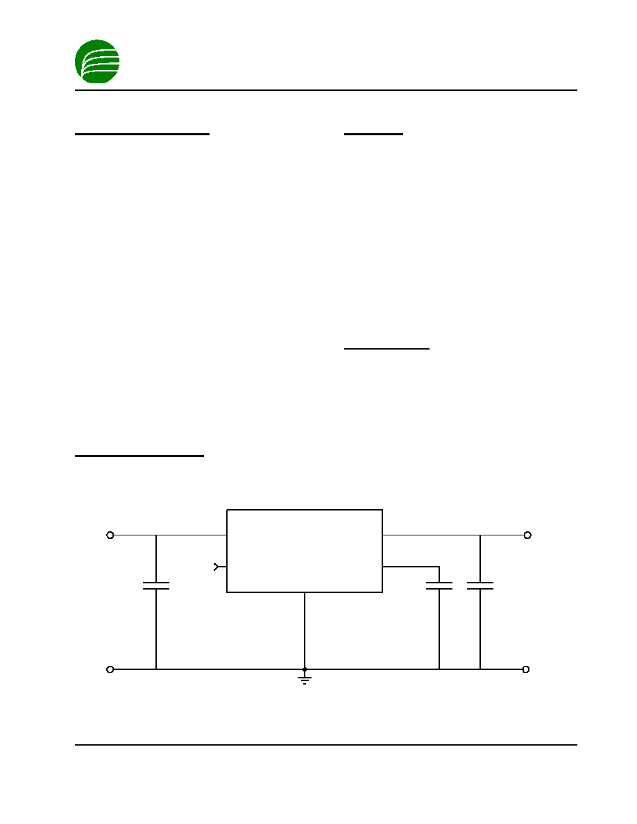
Typical Application
Preliminary Information
AAT3232
EN
V
IN
OUT
BYP
GND
ENABLE
1nF
INPUT
OUTPUT
C
IN
5.6
µ
F ceramic or
10
µ
F tantalum
1-43

AAT3232
300mA CMOS Low Drop Out Linear Regulator
Advanced Analogic Technologies, Inc.
1250 Oakmead Pkwy, Suite 310, Sunnyvale, CA 94086
(408)524-9684 Fax (408)524-9689
$1$/2*,&
7(&+
TM
3232.2000.05.0.98
Absolute Maximum Ratings
(T
A
=25
∞
C unless otherwise noted)
Symbol
Description
Max
Units
V
IN
Input Voltage
8
V
I
OUT
DC Output Current
P
D
/(V
IN
-V
O
)
mA
T
J
Operating Junction Temperature Range
150
∞
C
JA
Thermal Resistance (SOT-23-5)
260
∞
C/W
P
D
Maximum Power Dissipation (SOT-23-5)
380
mW
T
LEAD
Maximum Soldering Temperature (at leads, 10 sec)
300
∞
C
Note: Stresses above those listed in Absolute Maximum Ratings may cause permanent damage to the device. Functional operation at
conditions other than the operating conditions specified is not implied. Only one Absolute Maximum rating should be applied at any one
time.
Recommended Operating Conditions
Symbol
Description
Rating
Units
V
IN
Input Voltage
(V
OUT
+0.3) to 7
V
T
Ambient Temperature Range
-40 to +85
∞
C
Electrical Characteristics
(T
J
=25
∞
C unless otherwise noted)
Symbol
Description
Conditions
Min
Typ
Max
Units
V
OUT
Output Voltage
-1.5
1.5
%
I
OUT
Output Current
V
OUT
> 1.2V
300
mA
I
SC
Short Circuit Current
V
OUT
< 0.4V
300
mA
I
Q
Ground Current
V
IN
= 5V, no load
30
50
µ
A
I
SD
Shutdown Current
V
IN
= 5V, EN = low
1
µ
A
V
OUT
/
V
OUT
Line Regulation
I
OUT
= 5mA, V
IN
= V
OUT
+ 1
to V
OUT
+ 2
0.02
0.1
%
V
OUT
/
V
OUT
Load Regulation
I
OUT
= 1mA to 300mA
0.2
1
%
V
DO
Dropout Voltage
1
I
OUT
= 300mA
200
300
mV
V
ENL
Enable Threshold Low
0.5
V
V
ENH
Enable Threshold High
V
IN
-0.5
V
PSRR
Power Supply Rejection Ratio
1 kHz
55
dB
T
SD
Over Temp Shutdown Threshold
150
∞
C
T
HYS
Over Temp Shutdown Hysteresis
30
∞
C
e
N
Output Noise
20
µ
V
RMS
TC
Ouput Voltage Temp. Coeff.
40
ppm/
∞
C
Note 1: V
DO
is defined as V
IN
- V
OUT
when V
OUT
is 98% of nominal.
1-44
AAT3232
300mA CMOS Low Drop Out Linear Regulator
Advanced Analogic Technologies, Inc.
1250 Oakmead Pkwy, Suite 310, Sunnyvale, CA 94086
(408)524-9684 Fax (408)524-9689
$1$/2*,&
7(&+
TM
3232.2000.05.0.98
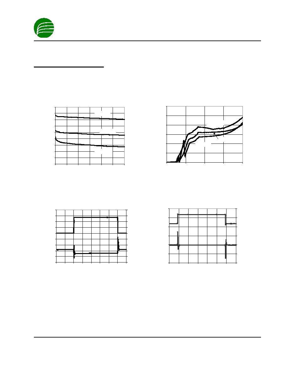
Typical Characteristics
(Unless otherwise noted, V
IN
= V
OUT
+ 1V, T
A
= 25
∞
C, C
NOISE
= 10nF, C
IN
= 2.0µF, C
OUT
= 5.6µF ceramic, I
OUT
= 100mA)
Output Voltage vs. Load Current
3.25
3.26
3.27
3.28
3.29
3.30
3.31
3.32
3.33
3.34
0
50
100
150
200
250
300
Iout (mA)
V
out (V
)
Ta = +125∞C
Ta = +25∞C
Ta = -40∞C
Ground Current vs. Input Voltage
0
10
20
30
40
50
60
0
2
4
6
8
Vin (volts)
I
gnd (
µ
A)
Ta = +125∞C
Ta = +25∞C
Ta = -40∞C
Step Load Transient Response
-20
-10
0
10
20
30
40
50
60
70
-200 -100
0
100 200 300 400 500 600
Time (us)
Output V
o
ltage
(mV
A
C
coupled)
-500
-400
-300
-200
-100
0
100
200
300
400
Load C
u
r
r
e
nt (mA
)
Line Transient Response
0
1
2
3
4
5
6
-100
0
100
200
300
400
500
600
Time (us)
Li
ne Vol
t
age (
V
)
-40
-20
0
20
40
60
80
O
u
t
put
Vol
t
age
(
m
V A
C
coupl
ed)
1-45
AAT3232
300mA CMOS Low Drop Out Linear Regulator
Advanced Analogic Technologies, Inc.
1250 Oakmead Pkwy, Suite 310, Sunnyvale, CA 94086
(408)524-9684 Fax (408)524-9689
$1$/2*,&
7(&+
TM
3232.2000.05.0.98
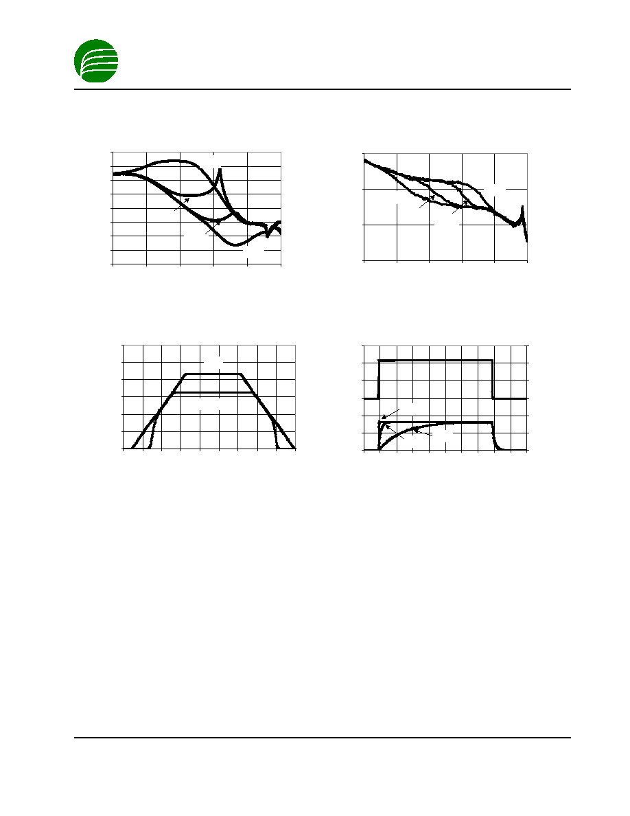
Power Supply Rejection Ratio
0
10
20
30
40
50
60
70
80
1.E+01
1.E+02
1.E+03
1.E+04
1.E+05
1.E+06
Frequency (Hz)
Rejectio
n
Ratio
(d
B)
100pF
1nF
10nF
None
Output Noise
0.01
0.1
1
10
1.E+01
1.E+02
1.E+03
1.E+04
1.E+05
1.E+06
Frequency (Hz)
No
i
s
e
(u
V /
Ro
o
t
Hz
)
100pF
1nF
10nF
None
Power-Up, Power-Down Response
0
1
2
3
4
5
6
-20
-10
0
10
20
30
40
50
60
70
Time (ms)
Vo
l
t
ag
e (V)
Output
Input
Turn On / Turn Off
0
2
4
6
8
10
12
-2
0
2
4
6
8
10
12
14
16
18
Time (ms)
O
u
t
p
u
t
V
o
lt
ag
e (
V
)
-6
-4
-2
0
2
4
6
En
ab
le (
V
)
10nF
1nF
100pF
1-46

AAT3232
300mA CMOS Low Drop Out Linear Regulator
Advanced Analogic Technologies, Inc.
1250 Oakmead Pkwy, Suite 310, Sunnyvale, CA 94086
(408)524-9684 Fax (408)524-9689
$1$/2*,&
7(&+
TM
3232.2000.05.0.98
Pin Descriptions
Pin #
Symbol
Function
1
V
IN
Input voltage pin ≠ should be decoupled with 1
µ
F or greater capacitor.
2
GND
Ground connection pin
3
EN
Enable pin ≠ pin is internally pulled high. When pulled low the PMOS pass transistor
turns off and the device enters low-power mode, consuming less than 1
µ
A.
4
BYP
Bypass capacitor connection -- to improve AC ripple rejection, connect a 1nF
capacitor to GND. This will also provide a soft start function.
5
OUT
Output pin ≠ should be decoupled with 2.2
µ
F or greater output capacitor. See
Detailed Description section for further information.
Functional Block Diagram
Over-Current
Protection
Over-Temp
Protection
V
REF
V
IN
EN
BYP
GND
OUT
1-47