
General Description
The AAT3687 BatteryManager is a member of
AnalogicTech's Total Power Management ICTM
(TPMICTM) product family. This device is a highly
integrated single-cell lithium-ion/polymer battery
charger IC designed to operate with AC adapter
inputs. It requires a minimum number of external
components. The AAT3687 precisely regulates
battery charge voltage and current for 4.2V lithium-
ion/polymer battery cells. Adapter charge current
rates can be programmed up to 1.5A. An active
thermal management system regulates the fast
charge constant current for all ambient tempera-
ture and input vs. output voltage conditions.
Battery temperature and charge state are fully
monitored for fault conditions. In the event of an
over-voltage or over-temperature failure, the
device will automatically shut down, thus protecting
the charging device, control system, and the bat-
tery under charge. Status monitor output pins are
provided to indicate the battery charge status by
directly driving two external LEDs. A serial interface
output is available to report 12 various charging
status states to a microcontroller.
The AAT3687 is available in a Pb-free, thermally-
enhanced, space-saving 12-pin TDFN 3x3mm
package and is rated over the -40∞C to +85∞C tem-
perature range.
Features
∑
Input Voltage Range: 4.0V to 5.5V
∑
Up to 1.5A Charging Current
∑
Adapter Present Indicator (ADPP#)
∑
High Level of Integration with Internal:
-- Charging Device
-- Reverse Blocking Diode
-- Current Sensing
∑
Active Thermal Loop Charge Reduction
∑
Automatic Recharge Sequencing
∑
Battery Temperature Monitoring
∑
Full Battery Charge Auto Turn-Off / Sleep Mode
∑
Over-Voltage, Over-Temperature, and
Emergency Thermal Protection
∑
Power On Reset and Soft Start
∑
Serial Interface Status Report
∑
12-Pin 3x3mm TDFN Package
∑
-40∞C to +85∞C Temperature Range
Applications
∑
Cellular Telephones
∑
Digital Still Cameras
∑
Hand Held PCs
∑
MP3 Players
∑
Personal Data Assistants (PDAs)
∑
Other Lithium-Ion/Polymer Battery-Powered
Devices
AAT3687
Lithium-Ion/Polymer Battery Charger
Typical Application
AAT3687
C
OUT
10
F
BATT-
TEMP
Battery
Pack
ADP
ADPSET
CT
GND
TS
BAT
BATT+
R
SET
R
B1
R
B2
C
IN
10
F
C
T
0.1
F
Adapter
STAT1
LED1
LED2
STAT2
DATA
Serial Interface
EN
Enable
ADPP#
Adapter
Present
+
3687.2006.06.1.5
1
BatteryManager
TM

Pin Descriptions
Pin Configuration
TDFN33-12
(Top View)
BAT
ADP
GND
1
EN
ADPP#
TS
ADPSET
N/C
CT
STAT1
STAT2
DATA
2
3
4
5
6
12
11
10
9
8
7
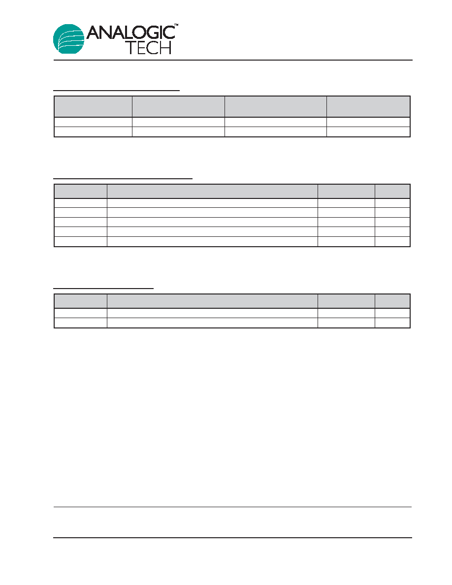
Pin # Name
Type
Function
1
BAT
Out
Battery charging and sensing.
2
ADP
In
Adapter input.
3
GND
Ground
Ground connection.
4
EN
In
AAT3687: Enable pin. Logic high enables the IC.
AAT3687-2: Enable pin. Logic high enables the IC. EN tied to internal
4M
pull-up resistor to ADP.
5
ADPP#
Out
Adapter present indicator. This pin is open drain until ADP pin reaches
threshold.
6
TS
In/Out
Connect to 10k
NTC thermistor.
7
DATA
Out
Status report to microcontroller via serial interface: open drain.
8
STAT2
Out
Battery charge status indicator pin to drive an LED: active low, open drain.
9
STAT1
Out
Battery charge status indicator pin to drive an LED: active low, open drain.
10
CT
In/Out
Timing capacitor to adjust internal watchdog timer. Set maximum charge
time for adapter powered trickle, CC, and CV charge modes. If timing
function is not needed, terminate this pin to ground.
11
N/C
No connection.
12
ADPSET
In/Out
Use resistor at this pin to set adapter charging current.
EP
Exposed paddle (bottom); connect to GND directly beneath package.
AAT3687
Lithium-Ion/Polymer Battery Charger
2
3687.2006.06.1.5
AAT3687 Feature Options
Absolute Maximum Ratings
1
Thermal Information
Symbol
Description
Value
Units
JA
Maximum Thermal Resistance
2
50
∞C/W
P
D
Maximum Power Dissipation
2.0
W
Symbol
Description
Value
Units
V
P
ADP Input Voltage, <30ms, Duty Cycle <10%
-0.3 to 7.0
V
V
P
ADP Input Voltage, Continuous
-0.3 to 6.0
V
V
N
BAT, TS, ADPSET, ADPP#, DATA, CT, EN, STAT1, STAT2
-0.3 to V
P
+ 0.3
V
T
J
Operating Junction Temperature Range
-40 to 150
∞C
T
LEAD
Maximum Soldering Temperature (at leads)
300
∞C
Internal Pull-Up
Can Leave
Product
Trickle Charge
Resistor on EN Pin
TS Pin Open
AAT3687
Yes
No
No
AAT3687-2
No
Yes
Yes
AAT3687
Lithium-Ion/Polymer Battery Charger
3687.2006.06.1.5
3
1. Stresses above those listed in Absolute Maximum Ratings may cause permanent damage to the device. Functional operation at condi-
tions other than the operating conditions specified is not implied. Only one Absolute Maximum Rating should be applied at any one time.
2. Mounted on an FR4 board.
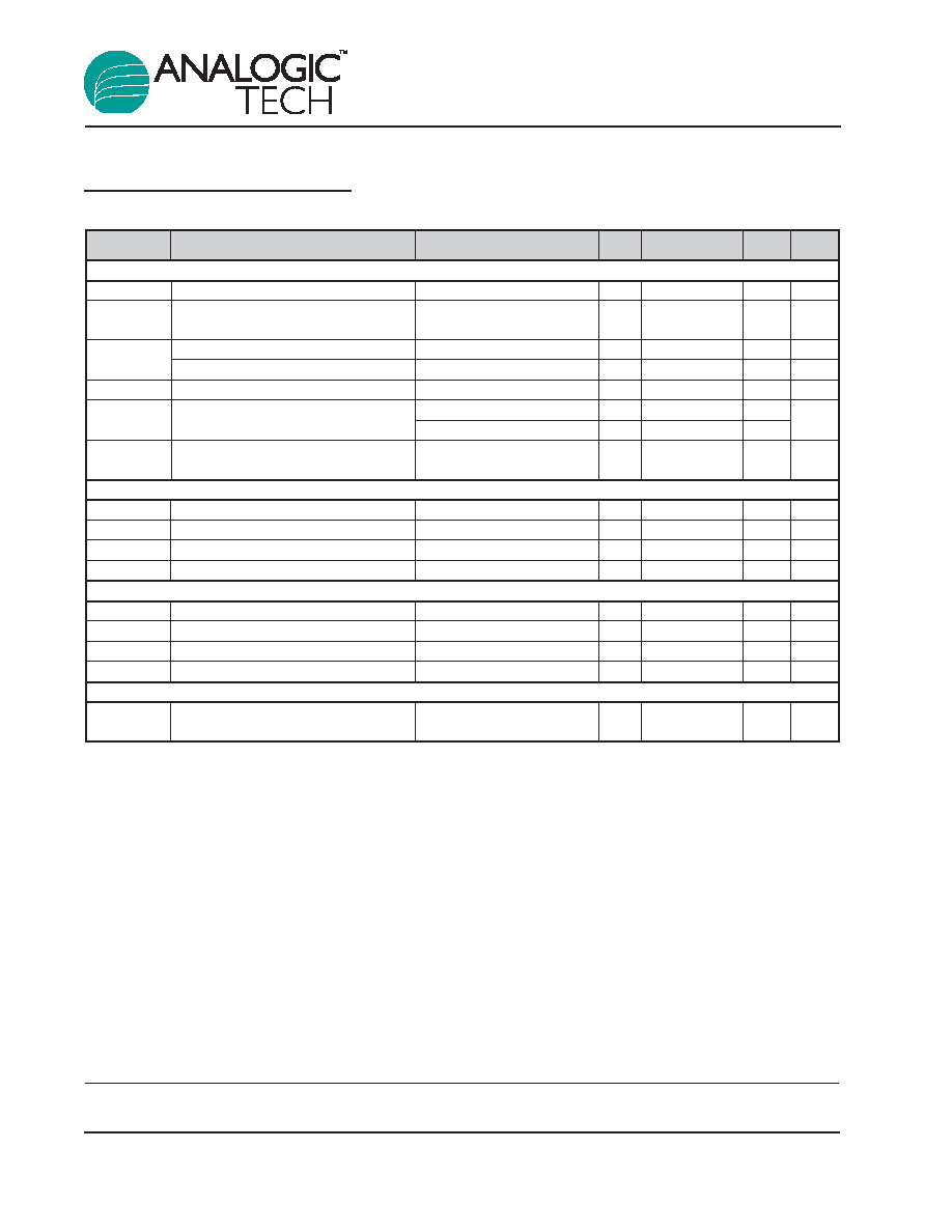
Electrical Characteristics
1
V
ADP
= 5V, T
A
= -25∞C to +85∞C, unless otherwise noted. Typical values are at T
A
= 25∞C.
Symbol
Description
Conditions
Min
Typ
Max Units
Operation
ADP
Adapter Voltage Range
4.0
5.5
V
V
ADPP
Adapter Present Indicator Threshold
4.25
4.5
4.7
V
Voltage
V
UVLO
Under-Voltage Lockout (UVLO)
Rising Edge
3.0
V
UVLO Hysteresis
150
mV
I
OP
Operating Current
Charge Current = 100mA
0.75
1.5
mA
I
SLEEP
Sleep Mode Current
AAT3687: V
BAT
= 4.25V
0.3
1.0
A
AAT3687-2: V
BAT
= 4.25V
1
3
I
Leakage
Reverse Leakage Current from
V
BAT
= 4V, ADP Pin Open
1.0
A
BAT Pin
Voltage Regulation
V
BAT_EOC
1
End of Charge Voltage Accuracy
4.158
4.20
4.242
V
V
CH
/V
CH
Output Charge Voltage Tolerance
0.5
%
V
MIN
Preconditioning Voltage Threshold
AAT3687 Only
2.8
3.0
3.15
V
V
RCH
Battery Recharge Voltage Threshold
V
BAT_EOC
- 0.1
V
Current Regulation
I
CH
Charge Current
100
1500
mA
I
CH
/I
CH
Charge Current Regulation Tolerance
10
%
V
ADPSET
ADPSET Pin Voltage
CC Mode
2.0
V
K
IA
Current Set Factor: I
CH
/I
ADPSET
4000
Charging Devices
R
DS(ON)
Adapter Charging Transistor
V
IN
= 5.5V
0.2
0.25
0.35
On Resistance
AAT3687
Lithium-Ion/Polymer Battery Charger
4
3687.2006.06.1.5
1. The AAT3687 output charge voltage is specified over the 0∞ to 70∞C ambient temperature range; operation over the -25∞C to +85∞C
temperature range is guaranteed by design.

Electrical Characteristics
1
V
ADP
= 5V, T
A
= -25∞C to +85∞C, unless otherwise noted. Typical values are at T
A
= 25∞C.
Symbol
Description
Conditions
Min
Typ
Max
Units
Logic Control / Protection
V
EN(H)
Input High Threshold
1.6
V
V
EN(L)
Input Low Threshold
0.4
V
I
EN(H)
EN Input Current
AAT3687-2 Only; V
EN
= 5V
10
A
V
ADPP#
Output Low Voltage
ADPP# Pin Sinks 500A
0.4
V
T
C
Preconditioning and Constant
C
CT
= 100nF, V
ADP
= 5.5V
3.0
Hours
Current Mode Time Out
T
P
Preconditioning Time Out
AAT3687 Only; C
CT
= 100nF,
25
Minutes
V
ADP
= 5.5V
T
V
Constant Voltage Mode Time Out
C
CT
= 100nF, V
ADP
= 5.5V
3.0
Hours
V
STAT
Output Low Voltage
STAT Pin Sinks 4mA
0.4
V
I
STAT
STAT Pin Current Sink Capability
8.0
mA
V
OVP
Over-Voltage Protection Threshold
4.4
V
I
TK
/I
CHG
Pre-Charge Current
AAT3687 Only
10
%
Charge Termination Threshold
7.5
%
Current I
TERM
/I
CHG
I
TS
Current Source from TS Pin
70
80
90
A
TS1
TS Hot Temperature Fault
Threshold
310
330
350
mV
Hysteresis
15
TS2
TS Cold Temperature Fault
Threshold
2.2
2.3
2.4
V
Hysteresis
10
mV
I
DATA
DATA Pin Sink Current
DATA Pin is Active Low State
3
mA
I
ADPP#
ADPP# Current Sink
ADPP# Pin is Active Low State
8
mA
V
DATA(H)
Input High Threshold
1.6
V
V
DATA(L)
Input Low Threshold
0.4
V
SQ
PULSE
Status Request Pulse Width
Status Request
200
ns
t
PERIOD
System Clock Period
50
s
f
DATA
Data Output Frequency
20
kHz
T
REG
Thermal Loop Regulation
90
∞C
T
LOOP_IN
Thermal Loop Entering Threshold
110
∞C
T
LOOP_OUT
Thermal Loop Exiting Threshold
85
∞C
T
OVSD
Over-Temperature Shutdown
145
∞C
Threshold
AAT3687
Lithium-Ion/Polymer Battery Charger
3687.2006.06.1.5
5
1. The AAT3687 output charge voltage is specified over the 0∞ to 70∞C ambient temperature range; operation over the -25∞C to +85∞C
temperature range is guaranteed by design.
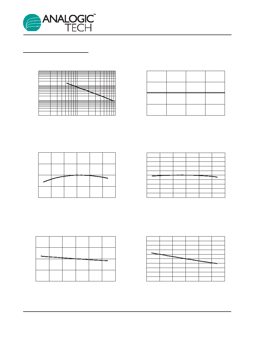
Typical Characteristics
Fast Charge Current vs. Temperature
(ADPSET = 8.06k
)
Temperature (
∞C)
I
CH
ADP (mA)
900
920
940
960
980
1000
1020
1040
1060
1080
1100
-50
-25
0
25
50
75
100
Preconditioning I
CH
vs. Temperature
(ADPSET = 8.06k
)
Temperature (
∞C)
I
CH
ADP (mA)
80
90
100
110
120
-50
-25
0
25
50
75
100
Preconditioning Threshold
Voltage vs. Temperature
Temperature (
∞
∞C)
V
MIN
(V)
2.95
2.96
2.97
2.98
2.99
3.00
3.01
3.02
3.03
3.04
3.05
-50
-25
0
25
50
75
100
End of Charge Voltage Regulation
vs. Temperature
Temperature (
∞
∞C)
V
BAT
(V)
4.158
4.179
4.200
4.221
4.242
-50
-25
0
25
50
75
100
Battery Voltage vs. Supply Voltage
Supply Voltage (V)
V
BAT
(V)
4.158
4.179
4.200
4.221
4.242
4.5
4.75
5.0
5.25
5.5
I
FASTCHARGE
vs. R
SET
R
SET
(k
)
I
FASTCHARGE
(mA)
10
100
1000
10000
1
10
100
AAT3687
Lithium-Ion/Polymer Battery Charger
6
3687.2006.06.1.5

Typical Characteristics
Counter Timeout vs. Temperature
(CT = 0.1
F)
Temperature (
∞C)
Counter Timeout (%)
-10
-8
-6
-4
-2
0
2
4
6
8
10
-50
-25
0
25
50
75
100
Adapter Mode Supply Current
vs. ADPSET Resistor
ADPSET Resistor (k
)
I
Q
(mA)
0.00
0.10
0.20
0.30
0.40
0.50
0.60
0.70
0.80
1
10
100
1000
Pre-Conditioning
Constant Current
V
IL
vs. Supply Voltage
EN Pin (Falling)
Supply Voltage (V)
V
IH
(V)
0.4
0.5
0.6
0.7
0.8
0.9
1.0
1.1
1.2
1.3
1.4
4.2
4.4
4.6
4.8
5.0
5.2
5.4
5.6
5.8
6.0
-40
∞C
+25
∞C
+85
∞C
V
IH
vs. Supply Voltage
EN Pin (Rising)
Supply Voltage (V)
V
IH
(V)
0.4
0.5
0.6
0.7
0.8
0.9
1.0
1.1
1.2
1.3
1.4
4.2
4.4
4.6
4.8
5.0
5.2
5.4
5.6
5.8
6.0
-40
∞C
+25
∞C
+85
∞C
Fast Charge Current vs. Supply Voltage
(ADPSET = 8.06k
)
Supply Voltage (V)
I
CH
(mA)
0
200
400
600
800
1000
1200
4.0
4.5
5.0
5.5
6.0
V
BAT
= 3.3V
V
BAT
= 3.5V
V
BAT
= 3.9V
Charging Current vs. Battery Voltage
(ADPSET = 8.06k
; V
IN
= 5.0V)
Battery Voltage (V)
I
CH
(A)
0.0
0.2
0.4
0.6
0.8
1.0
1.2
2.5
2.9
3.3
3.7
4.1
4.5
AAT3687
Lithium-Ion/Polymer Battery Charger
3687.2006.06.1.5
7

Typical Characteristics
Temperature Sense Output Current
vs. Temperature
Temperature (
∞
∞C)
TS Pin Current (
A)
72
74
76
78
80
82
84
86
88
-50
-25
0
25
50
75
100
CT Pin Capacitance vs. Counter Timeout
Time (hours)
Capacitance (
F)
0.0
0.2
0.4
0.6
0.8
1.0
1.2
1.4
1.6
1.8
2.0
0
2
4
6
8
10
Precondition Timeout
Precondition + Constant Current Timeout
or Constant Voltage Timeout
AAT3687
Lithium-Ion/Polymer Battery Charger
8
3687.2006.06.1.5

AAT3687
Lithium-Ion/Polymer Battery Charger
3687.2006.06.1.5
9
Functional Block Diagram
Charge
Control
Reverse Blocking
CV/
Precharge
1
Constant
Current
Current
Compare
ADP
BAT
ADPSET
UVLO
Over-
Temperature
Protection
Charge
Status
STAT2
STAT1
TS
Window
Comparator
80A
4.2V
Serial
Data
DATA
Watchdog
Timer
CT
Voltage
Sense
ADPP#
EN
GND
IC enable
Functional Description
The AAT3687 is a highly integrated single-cell lithium-
ion/polymer battery charger IC designed to operate
with standard AC adapter input sources, while requir-
ing a minimum number of external components. The
AAT3687 precisely regulates battery charge voltage
and current for 4.2V lithium-ion/polymer battery cells.
The adapter charge input constant current level can
be programmed up to 1.5A for rapid charging appli-
cations. The AAT3687 is rated for operation from -
40∞C to +85∞C. In the event of operating ambient
temperatures exceeding the power dissipation abili-
ties of the device package for a given constant current
charge level, the charge control will enter into thermal
regulation. When the system thermal regulation
becomes active, the programmed constant current
charge amplitude will be automatically reduced to a
safe level for the current operating condition. Should
the ambient operating temperature drop below the
thermal loop threshold, the system will automatically
resume charging at the full programmed constant cur-
rent level. This intelligent thermal management sys-
tem permits the AAT3687 to operate and safely
charge a battery cell over a wide range of ambient
conditions while maximizing the greatest possible
charge current for the given set of conditions.
Status monitor output pins are provided to indicate
the battery charge state by directly driving two exter-
nal LEDs. A serial interface output is also available to
report any one of 12 distinct charge states to the sys-
tem microcontroller.
Battery temperature and charge state are fully moni-
tored for fault conditions. In the event of an over-volt-
age or over-temperature failure, the device will auto-
matically shut down, thus protecting the charging
device, control system, and the battery under charge.
In addition to internal charge controller thermal pro-
tection, the AAT3687 also provides a temperature
sense feedback function (TS pin) from the battery to
shut down the device in the event the battery
exceeds its own thermal limit during charging. All
fault events are reported to the user either by the
simple status LEDs or via the DATA pin function.
1. Precharge applies to AAT3687 only.

AAT3687
Lithium-Ion/Polymer Battery Charger
10
3687.2006.06.1.5
Charging Operation
The AAT3687 has four basic modes for the battery
charge cycle: pre-conditioning / trickle charge; con-
stant current / fast charge; constant voltage; and
end of charge (see Figure 1.) (AAT3687-2 does not
have trickle charge.)
Battery Preconditioning
Before the start of charging, the AAT3687 checks
several conditions in order to assure a safe charging
environment. The input supply must be above the
minimum operating voltage, or under-voltage lockout
threshold (V
UVLO
), for the charging sequence to
begin. Also, the cell temperature, as reported by a
thermistor connected to the TS pin from the battery,
must be within the proper window for safe charging.
When these conditions have been met and a battery
is connected to the BAT pin, the AAT3687 checks the
state of the battery. If the cell voltage is below the
preconditioning voltage threshold (V
MIN
), the charge
control begins preconditioning the cell.
The battery preconditioning trickle charge current is
equal to the fast charge constant current divided by
10. For example, if the programmed fast charge
current is 1.5A, then the preconditioning mode
(trickle charge) current will be 150mA. Cell precon-
ditioning is a safety precaution for deeply dis-
charged battery cells and also aids in limiting power
dissipation in the pass transistor when the voltage
across the device is at the greatest potential.
Fast Charge / Constant Current Charging
Battery cell preconditioning continues until the volt-
age on the BAT pin exceeds the preconditioning
voltage threshold (V
MIN
). At this point, the AAT3687
begins the constant current fast charging phase.
The fast charge constant current (I
CC
) amplitude is
programmed by the user via the R
SET
, resistor. The
AAT3687 remains in the constant current charge
mode until the battery reaches the voltage regula-
tion point, V
BAT
.
Constant Voltage Charging
The system transitions to a constant voltage charg-
ing mode when the battery voltage reaches the
output charge regulation threshold (V
BAT
) during
the constant current fast charge phase. The regu-
lation voltage level is factory programmed to 4.2V
(±1%). Charge current in the constant voltage
mode drops as the battery cell under charge reach-
es its maximum capacity.
End of Charge Cycle Termination and Recharge
Sequence
When the charge current drops to 7.5% of the pro-
grammed fast charge current level in the constant
voltage mode, the device terminates charging and
goes into a sleep state. The charger will remain in
a sleep state until the battery voltage decreases to
a level below the battery recharge voltage thresh-
old (V
RCH
).
When the input supply is disconnected, the charg-
er will automatically transition into a power-saving
sleep mode. Only consuming an ultra-low 0.3A in
sleep mode (1A for AAT3687-2), the AAT3687
minimizes battery drain when it is not charging.
This feature is particularly useful in applications
where the input supply level may fall below the bat-
tery charge or under-voltage lockout level. In such
cases where the AAT3687 input voltage drops, the
device will enter sleep mode and automatically
resume charging once the input supply has recov-
ered from the fault condition.
Figure 1: Current vs. Voltage Profile During Charging Phases.
Constant Current
Charge Phase
Constant Voltage
Charge Phase
Preconditioning
Trickle Charge
Phase
Charge Complete Voltage
Constant Current Mode
Voltage Threshold
Regulated Current
Trickle Charge and
Termination Threshold
I = CC / 10
I = Max CC
AAT3687
Lithium-Ion/Polymer Battery Charger
3687.2006.06.1.5
11
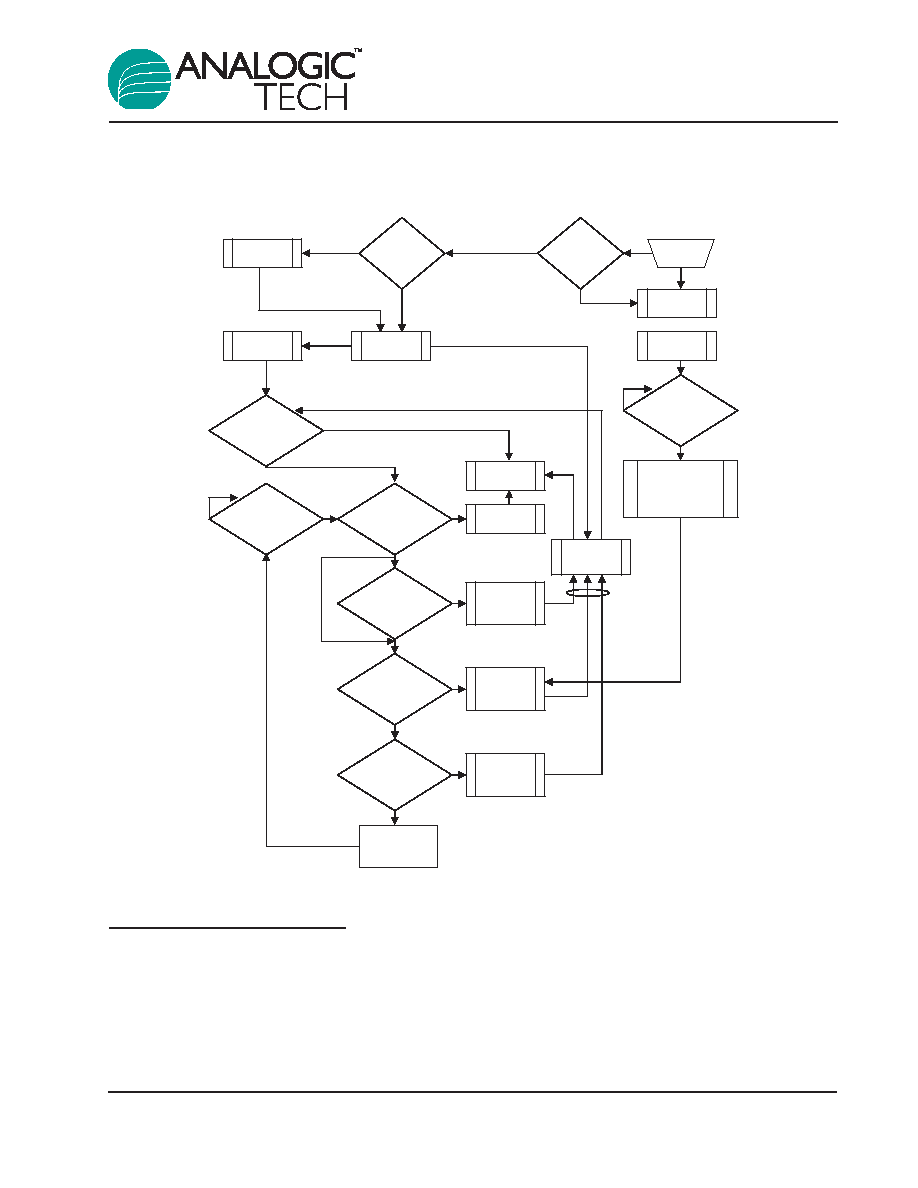
System Operation Flow Chart
No
No
Yes (AAT3687)
Yes (AAT3687-2)
Yes
No
No
Yes
No
Yes
No
Yes
Yes
Charge
Completed
Voltage Phase Test
I
BAT
> I
MIN
Current Phase Test
V
CH
> V
BAT
Preconditioning Test
V
MIN
> V
BAT
Recharge Test
V
RCH
> V
BAT
Battery
Temperature Monitor
V
TS1
< TS < V
TS2
Voltage
Charging
Mode
Current
Charging
Mode
Low Current
Conditioning
Battery
Temperature
Shut Down
Yes
Set
Expire
No
Yes
Yes
No
Timing
No
Yes
No
Enable
Charge
Safety Timer
Thermal Loop
Current
Reduction
Thermal
Loop
Sleep
Mode
Switch
Device
Temperature
Monitor
T
J
> 110
∞C
Fault
Conditions Monitor
OV, OT
ADP
Loop
ADP
Voltage
ADP > V
ADPP
UVLO
V
P
> V
UVLO
Power On
Reset
Output
ADPP
Application Information
Adapter Power Input
Constant current charge levels up to 1.5A may be
programmed by the user when powered from a suf-
ficient input power source. The AAT3687 will oper-
ate from the adapter input over a 4.0V to 5.5V
range.
The constant current fast charge current for the
adapter input is set by the R
SET
resistor connected
between the ADPSET and ground. Refer to Table 1
for recommended R
SET
values for a desired con-
stant current charge level. The presence of voltage
on the adapter input is indicated by the ADPP# pin
function. This indicator pin uses an internal open
drain device that will pull the ADPP# pin low when

AAT3687
Lithium-Ion/Polymer Battery Charger
12
3687.2006.06.1.5
voltage is detected on the ADP pin. The precise
charging function of the AAT3687 may be read from
the DATA pin and/or status LEDs. Please refer to
the Battery Charge Status Indication discussion for
further details on data reporting.
Thermal Loop Control
Due to the integrated nature of the linear charging
control pass device for the adapter input, a special
thermal loop control system has been employed to
maximize charging current under all operating con-
ditions. The thermal management system meas-
ures the internal circuit die temperature and reduces
the fast charge current when the device exceeds a
preset internal temperature control threshold. Once
the thermal loop control becomes active, the fast
charge current is initially reduced by a factor of 0.44.
The initial thermal loop current can be estimated by
the following equation:
Eq. 1:
The thermal loop control re-evaluates the circuit die
temperature in 330ms intervals and adjusts the fast
charge current back up in small steps to the full fast
charge current level or until an equilibrium current
is discovered and maximized for the given ambient
temperature condition. The thermal loop controls
the system charge level; therefore, the AAT3687
will always provide the highest level of constant
current in the fast charge mode possible for any
given ambient temperature condition.
Adapter Input Charge Inhibit and Resume
The AAT3687 has a UVLO and power on reset fea-
ture so that the charger will suspend charging and
shut down if the input supply to the adapter pin
drops below the UVLO threshold. When power is
re-applied to the adapter pin or the UVLO condi-
tions recovers, the system charge control will
assess the state of charge on the battery cell and
will automatically resume charging in the appropri-
ate mode for the condition of the battery.
Enable / Disable
The AAT3687 provides an enable function to control
the charger IC on and off. The enable (EN) pin is
active high. When pulled to a logic low level, the
AAT3687 will be shut down and forced into the sleep
state. Charging will be halted regardless of the bat-
tery voltage or charging state. When the device is re-
enabled, the charge control circuit will automatically
reset and resume charging functions with the appro-
priate charging mode based on the battery charge
state and measured cell voltage on the BAT pin.
Programming Charge Current
The fast charge constant current charge level is
user programmed with a set resistor placed
between the ADPSET pin and ground. The accu-
racy of the fast charge, as well as the precondi-
tioning trickle charge current, is dominated by the
tolerance of the set resistor used. For this reason,
a 1% tolerance metal film resistor is recommended
for the set resistor function.
Fast charge constant current levels from 50mA to
1.5A can be set by selecting the appropriate resis-
tor value from Table 1.
Table 1: Recommended R
SET
Values.
ADP
ADP
I
CC
R
SET
(k
)
I
CC
R
SET
(k
)
50
N/A
800
10.2
75
N/A
900
9.09
100
84.5
1000
8.06
200
43.2
1100
7.32
300
28.0
1200
6.65
400
21.0
1300
6.04
500
16.9
1400
5.62
600
13.3
1500
5.36
700
11.5
I
TLOOP
= I
CC
∑ 0.44

AAT3687
Lithium-Ion/Polymer Battery Charger
3687.2006.06.1.5
13
Figure 2: I
FASTCHARGE
vs. R
SET
.
Protection Circuitry
Programmable Watchdog Timer
The AAT3687 contains a watchdog timing circuit to
shut down charging functions in the event of a defec-
tive battery cell not accepting a charge over a preset
period of time. Typically, a 0.1F ceramic capacitor
is connected between the CT pin and ground. When
a 0.1F ceramic capacitor is used, the device will
time out a shutdown condition if the trickle charge
mode exceeds 25 minutes (AAT3687 only) and a
combined trickle charge plus fast charge mode of 3
hours. When the device transitions to the constant
voltage mode, the timing counter is reset and will
time out after an additional 3 hours if the charge cur-
rent does not drop to the charge termination level.
Table 2: Summary for a 0.1F Ceramic
Capacitor Used for the Timing Capacitor.
The CT pin is driven by a constant current source
and will provide a linear response to increases in the
timing capacitor value. Thus, if the timing capacitor
were to be doubled from the nominal 0.1F value,
the time-out periods would be doubled.
If the programmable watchdog timer function is not
needed, it can be disabled by terminating the CT
pin to ground. The CT pin should not be left float-
ing or un-terminated, as this will cause errors in the
internal timing control circuit.
The constant current provided to charge the timing
capacitor is very small, and this pin is susceptible
to noise and changes in capacitance value.
Therefore, the timing capacitor should be physical-
ly located on the printed circuit board layout as
close as possible to the CT pin. Since the accura-
cy of the internal timer is dominated by the capaci-
tance value, a 10% tolerance or better ceramic
capacitor is recommended. Ceramic capacitor
materials, such as X7R and X5R types, are a good
choice for this application.
Over-Voltage Protection
An over-voltage event is defined as a condition
where the voltage on the BAT pin exceeds the
maximum battery charge voltage and is set by the
over-voltage protection threshold (V
OVP
). If an
over-voltage condition occurs, the AAT3687 charge
control will shut down the device until the voltage
on the BAT pin drops below V
OVP
. The AAT3687
will resume normal charging operation after the
over-voltage condition is removed. During an over-
voltage event, the STAT LEDs will report a system
fault, and the actual fault condition can be read via
the DATA pin signal.
Over-Temperature Shutdown
The AAT3687 has a thermal protection control cir-
cuit which will shut down charging functions should
the internal die temperature exceed the preset
thermal limit threshold.
Battery Temperature Fault Monitoring
In the event of a battery over-temperature condi-
tion, the charge control will turn off the internal pass
device and report a battery temperature fault on the
DATA pin function. The STAT LEDs will also dis-
play a system fault. After the system recovers from
a temperature fault, the device will resume charg-
ing operation.
The AAT3687 checks battery temperature before
starting the charge cycle, as well as during all
stages of charging. This is accomplished by moni-
toring the voltage at the TS pin. This system is
intended for use with negative temperature coeffi-
cient thermistors (NTC) which are typically inte-
grated into the battery package. Most of the com-
monly used NTC thermistors in battery packs are
Mode
Time
Trickle Charge (TC) Time Out
25 minutes
(AAT3687 only)
Trickle Charge (TC) +
3 hours
Fast Charge (CC) Time Out
Constant Voltage (VC) Mode
3 hours
Time Out
R
SET
(k
)
I
FASTCHARGE
(mA)
10
100
1000
10000
1
10
100

AAT3687
Lithium-Ion/Polymer Battery Charger
14
3687.2006.06.1.5
approximately 10k
at room temperature (25∞C).
The TS pin has been specifically designed to
source 80A of current to the thermistor. The volt-
age on the TS pin resulting from the resistive load
should stay within a window of 335mV to 2.32V. If
the battery becomes too hot during charging due to
an internal fault or excessive fast charge current,
the thermistor will heat up and reduce in value,
pulling the TS pin voltage lower than the TS1
threshold, and the AAT3687 will signal the fault
condition.
If the use of the TS pin function is not required by
the system, it should be terminated to ground using
a 10k
resistor. Alternatively, on the AAT3687-2,
the TS pin may be left open.
Battery Charge Status Indication
The AAT3687 indicates the status of the battery
under charge with two different systems. First, the
device has two status LED driver outputs. These
two LEDs can indicate simple functions such as no
battery charge activity, battery charging, charge
complete, and charge fault. The AAT3687 also
provides a bi-directional data reporting function so
that a system microcontroller can interrogate the
DATA pin and read any one of 12 system states.
Status Indicator Display
Simple system charging status states can be dis-
played using one or two LEDs in conjunction with
the STAT1 and STAT2 pins on the AAT3687.
These two pins are simple open drain switches
used to connect the LED cathodes to ground. It is
not necessary to use both display LEDs if a user
simply wants to have a single lamp to show "charg-
ing" or "not charging."
This can be accomplished by using the STAT1 pin
and a single LED. Using two LEDs and both STAT
pins simply gives the user more information to the
charging states. Refer to Table 3 for LED display
definitions. The LED anodes should be connected
to V
ADP
.
The LEDs should be biased with as little current as
necessary to create reasonable illumination; there-
fore, a ballast resistor should be placed between
the LED cathodes and the STAT1/2 pins. LED cur-
rent consumption will add to the overall thermal
power budget for the device package, hence it is
good to keep the LED drive current to a minimum.
2mA should be sufficient to drive most low-cost
green or red LEDs. It is not recommended to
exceed 8mA for driving an individual status LED.
The required ballast resistor values can be esti-
mated using the following formulas:
Eq. 2:
Example:
Eq. 3:
Note: Red LED forward voltage (V
F
) is typically
2.0V @ 2mA
(5.5V - 2.0V)
R
B(STAT1)
=
= 1.75k
2mA
(V
ADP
-
V
F(LED)
)
R
B(STAT1/2)
=
I
LED(STAT1/2)
Table 3: LED Status Indicator.
Event Description
STAT1
STAT2
Charge Disabled or Low Supply
Off
Off
Charge Enabled Without Battery
Flash
1
Flash
1
Battery Charging
On
Off
Charge Completed
Off
On
Fault
On
On
1. Flashing rate depends on output capacitance.
AAT3687
Lithium-Ion/Polymer Battery Charger
3687.2006.06.1.5
15
Data Timing
The system microcontroller should assert an active
low data request pulse for minimum duration of
200ns; this is specified by T
LO(DATA)
. Upon sensing
the rising edge of the end of the data request pulse,
the AAT3687 status data control will reply the data
word back to the system microcontroller after a
delay specified by the data report time specification
T
DATA(RPT)
. The period of the following group of
data pulses will be specified by T
DATA
.
Digital Charge Status Reporting
The AAT3687 has a comprehensive digital data
reporting system by use of the DATA pin feature.
This function can provide detailed information
regarding the status of the charging system. The
DATA pin is a bi-directional port which will read
back a series of data pulses when the system
microcontroller asserts a request pulse. This sin-
gle strobe request protocol will invoke one of 12
possible return pulse counts that the system micro-
controller can look up based on the serial report
data listed in Table 4.
The DATA pin function logic is active low and
should normally be pulled high to V
ADP
. This data
line can also be pulled high to the same level as the
high state for the logic I/O port on the system
microcontroller. In order for the DATA pin control
circuit to generate clean, sharp edges for the data
output, and to maintain the integrity of the data tim-
ing for the system, the pull-up resistor on the data
line should be low enough in value so that the
DATA signal returns to the high state without delay.
If the pull-up resistor is too high, the strobe pulse
from the system microcontroller could exceed the
maximum pulse time and the DATA output control
could issue false status reports. A 1.5k
resistor is
recommended when pulling the DATA pin high to
5.0V on the V
ADP
input. If the data line is pulled
high to a voltage level less than 5.0V, the pull-up
resistor can be calculated based on a recommend-
ed minimum pull-up current of 3mA. Use the fol-
lowing formula:
Eq. 4:
V
PULL-UP
R
PULL-UP
3mA
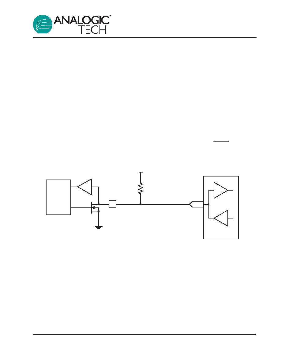
Figure 3: Data Pin Application Circuit.
AAT3687
Status
Control
1.8V to 5.0V
DATA Pin
R
PULL_UP
P GPIO
Port
GPIO
IN
IN
OUT
OUT

AAT3687
Lithium-Ion/Polymer Battery Charger
16
3687.2006.06.1.5
Timing Diagram
Table 4: Serial Data Report Table.
N
DATA Report Status
1
Chip Over-Temperature Shutdown.
2
Battery Temperature Fault.
3
Over-Voltage Turn Off.
4
Not Used.
5
ADP Watchdog Time-Out in Battery Condition Mode.
6
ADP Battery Condition Mode.
7
ADP Watchdog Time-Out in Constant Current Mode.
8
ADP Thermal Loop Regulation in Constant Current Mode.
9
ADP Constant Current Mode.
10
ADP Watchdog Time-Out in Constant Voltage Mode.
11
ADP Constant Voltage Mode.
12
ADP End of Charging.
23
Data Report Error.
SQ
SQ
PULSE
Data
System Reset
System Start
CK
T
SYNC
T
LAT
N=1
N=2
N=3
T
OFF
T
DATA(RPT)
= T
SYNC
+ T
LAT
< 2.5 P
DATA
T
OFF
> 2 P
DATA
P
DATA

AAT3687
Lithium-Ion/Polymer Battery Charger
3687.2006.06.1.5
17
Thermal Considerations
The AAT3687 is offered in a 3x3mm TDFN pack-
age which can provide up to 2.0W of power dissi-
pation when it is properly bonded to a printed cir-
cuit board and has a maximum thermal resistance
of 50∞C/W. Many considerations should be taken
into account when designing the printed circuit
board layout, as well as the placement of the
charger IC package in proximity to other heat gen-
erating devices in a given application design. The
ambient temperature around the charger IC will
also have an effect on the thermal limits of a bat-
tery charging application. The maximum limits that
can be expected for a given ambient condition can
be estimated by the following discussion.
First, the maximum power dissipation for a given
situation should be calculated:
Eq. 5:
Where:
P
D
= Total Power Dissipation by the Device
V
IN
= Input Voltage Amplitude, V
ADP
V
BAT
= Battery Voltage as Seen at the BAT Pin
I
CC
= Maximum Constant Fast Charge Current
Programmed for the Application
I
OP
= Quiescent Current Consumed by the
Charger IC for Normal Operation
Next, the maximum operating ambient temperature
for a given application can be estimated based on
the thermal resistance of the 3x3mm TDFN pack-
age when sufficiently mounted to a PCB layout and
the internal thermal loop temperature threshold.
Eq. 6:
Where:
T
A
= Ambient Temperature in ∞C
T
J
=
Maximum Device Junction Temperature
Below the Thermal Loop Threshold
P
D
= Total Power Dissipation by the Device
JA
= Package Thermal Resistance in ∞C/W
Example:
For an application where the fast charge current for
the adapter mode is set to 1A, V
ADP
= 5.0V and the
battery voltage at 3.6V, what is the maximum ambi-
ent temperature at which the thermal loop will
become active?
Given:
V
ADP
= 5.0V
V
BAT
= 3.6V
I
CC
= 1A
I
OP
= 0.75mA
T
J
= 110∞C
JA
= 50∞C/W
Using Equation 5, calculate the device power dissi-
pation for the stated condition:
Eq. 7:
The maximum ambient temperature before the
AAT3687 thermal loop becomes active can now be
calculated using Equation 6:
Eq. 8:
Therefore, under the stated conditions for this
worst case power dissipation example, the
AAT3687 will enter the thermal loop and lower the
fast charge constant current when the ambient
operating temperature rises above 39.8∞C.
T
A
= 110
∞C - (50∞C/W ∑ 1.40375W)
= 39.8125
∞C
P
D
= (5.0V - 3.6V)
(1A) + (5.0V
∑ 0.75mA)
= 1.40375W
T
A
= T
J
- (
JA
∑ P
D
)
P
D
= [(V
IN
- V
BAT
)
∑ I
CC
+ (V
IN
∑ I
OP
)]
AAT3687
Lithium-Ion/Polymer Battery Charger
18
3687.2006.06.1.5
Capacitor Selection
Input Capacitor
In general, it is good design practice to place a
decoupling capacitor between the ADP pin and
ground. An input capacitor in the range of 1F to
22F is recommended. If the source supply is
unregulated, it may be necessary to increase the
capacitance to keep the input voltage above the
under-voltage lockout threshold during device
enable and when battery charging is initiated.
If the AAT3687 adapter input is to be used in a sys-
tem with an external power supply source, such as
a typical AC-to-DC wall adapter, then a C
IN
capac-
itor in the range of 10F should be used. A larger
input capacitor in this application will minimize
switching or power transient effects when the
power supply is "hot plugged" in.
Output Capacitor
The AAT3687 only requires a 1F ceramic capaci-
tor on the BAT pin to maintain circuit stability. This
value should be increased to 10F or more if the
battery connection is made any distance from the
charger output. If the AAT3687 is to be used in
applications where the battery can be removed
from the charger, such as with desktop charging
cradles, an output capacitor greater than 10F may
be required to prevent the device from cycling on
and off when no battery is present.
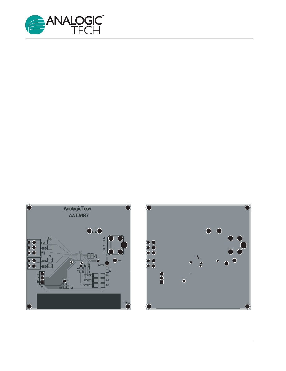
Printed Circuit Board Layout
Considerations
For the best results, it is recommended to physi-
cally place the battery pack as close as possible to
the AAT3687 BAT pin. To minimize voltage drops
on the PCB, keep the high current carrying traces
adequately wide. For maximum power dissipation
of the AAT3687 3x3mm TDFN package, the metal
substrate should be solder bonded to the board. It
is also recommended to maximize the substrate
contact to the PCB ground plane layer to further
increase local heat dissipation. Refer to the
AAT3687 evaluation board for a good layout exam-
ple (see Figures 4 and 5).
AAT3687 Evaluation Board Layout
Figure 4: AAT3687 Evaluation Board
Figure 5: AAT3687 Evaluation Board
Component Side Layout.
Solder Side Layout.

AAT3687
Lithium-Ion/Polymer Battery Charger
3687.2006.06.1.5
19
AAT3687 Evaluation Board Schematic Diagram
D2
D1
RED
LED
RED
LED
GRN
LED
D3
Open
R1
C1
10
F
C2
10
F
R2
10k
R6
8.06k
R7
1k
R5
4.99k
R4
4.99k
R3
4.99k
C3
0.1
F
SW1
DATA
CT
1 2 3
ON/OFF
J1
1
2
1
2
3
ADP
BAT
TS
GND
GND
BAT
1
ADP
2
GND
3
10
EN
4
ADPP#
5
TS
6
DATA
7
STAT2
8
STAT1
9
CT
ADPSET
12
AAT3687
U1
(TDFN33-12)
AAT3687
Lithium-Ion/Polymer Battery Charger
20
3687.2006.06.1.5
AAT3687 Evaluation Board Bill of Materials (BOM)
Quantity Description
Desig.
Footprint
Manufacturer
Part Number
1
Test Pin
DATA
PAD
Mill-Max
6821-0-0001-00-00-08-0
1
Connecting Terminal Block,
ADP, GND
TBLOK2
Phoenix Contact
277-1274-ND
2.54mm, 2 Position
1
Connecting Terminal Block,
BAT,
TBLOK3
Phoenix Contact
277-1273-ND
2.54mm, 3 Position
GND, TS
2
Capacitor, Ceramic, 10F C1,
C2
0805
Murata
490-1717-1-ND
6.3V 10% X5R 0805
1
Capacitor, Ceramic, 1F C3
0603
Murata
478-1244-2-ND
10% 25V X5R 0603
2
Typical Red LED, Ultra-Bright
D1, D3
1206LED
Chicago Miniature CMD15-21SRC/TR8
Lamp
1
Typical Green LED
D2
1206LED
Chicago Miniature CMD15-21VGC/TR8
Lamp
1
Header, 3-Pin
J1
HEADER2MM-3 Sullins
6821-0-0001-00-00-08-0
1
Resistor, 10k
, 1/16W
R2
0603
Panasonic/ECG
P10KCFCT-ND
5% 0603 SMD
3
Resistor, 4.99k
, 1/16W
R3, R4, R5
0603
Panasonic/ECG
P4.99KHTR-ND
1% 0603 SMD
1
Resistor, 8.06k
, 1/16W
R6
0603
Panasonic/ECG
P8.06KHCT-ND
1% 0603 SMD
1
Resistor, 1k
, 1/16W
R7
0603
Panasonic/ECG
P1.0KCGCT-ND
5% 0603 SMD
1
Switch Tact 6mm SPST
SW1
Switch
ITT Industries/
CKN9012-ND
H = 5.0mm
C&K Div
1
AAT3687 Lithium-Ion/Polymer
U1
TDFN33-12
AnalogicTech
AAT3687IWP-4.2
Battery Charge Controller

AAT3687
Lithium-Ion/Polymer Battery Charger
3687.2006.06.1.5
21
Ordering Information
Package Information
All dimensions in millimeters.
Top View
Bottom View
Detail "B"
Detail "A"
Side View
3.00
± 0.05
Index Area
(D/2 x E/2)
Detail "A"
Detail "B"
1.70
± 0.05
3.00
±
0.05
0.05
± 0.05
0.229
±
0.051
7.5
∞ ± 7.5∞
2.40
±
0.05
0.16
Pin 1 Indicator
(optional)
0.375
± 0.125
0.3
± 0.10
0.45
±
0.05
0.23
±
0.05
0.075
± 0.075
0.1 REF
0.8
+
0.05 -0.20
Option A:
C0.30 (4x) max
Chamfered corner
Option B:
R0.30 (4x) max
Round corner
All AnalogicTech products are offered in Pb-free packaging. The term "Pb-free" means
semiconductor products that are in compliance with current RoHS standards, including
the requirement that lead not exceed 0.1% by weight in homogeneous materials. For more
information, please visit our website at http://www.analogictech.com/pbfree.
Trickle Charge
Package
Marking
1
Part Number (Tape and Reel)
2
Yes
TDFN33-12
PIXYY
AAT3687IWP-4.2-T1
No
TDFN33-12
RTXYY
AAT3687IWP-4.2-2-T1
1. XYY = assembly and date code.
2. Sample stock is generally held on part numbers listed in BOLD.

AAT3687
Lithium-Ion/Polymer Battery Charger
22
3687.2006.06.1.5
Advanced Analogic Technologies, Inc.
830 E. Arques Avenue, Sunnyvale, CA 94085
Phone (408) 737-4600
Fax (408) 737-4611
© Advanced Analogic Technologies, Inc.
AnalogicTech cannot assume responsibility for use of any circuitry other than circuitry entirely embodied in an AnalogicTech product. No circuit patent licenses, copyrights, mask work rights,
or other intellectual property rights are implied. AnalogicTech reserves the right to make changes to their products or specifications or to discontinue any product or service without notice.
Customers are advised to obtain the latest version of relevant information to verify, before placing orders, that information being relied on is current and complete. All products are sold sub-
ject to the terms and conditions of sale supplied at the time of order acknowledgement, including those pertaining to warranty, patent infringement, and limitation of liability. AnalogicTech
warrants performance of its semiconductor products to the specifications applicable at the time of sale in accordance with AnalogicTech's standard warranty. Testing and other quality con-
trol techniques are utilized to the extent AnalogicTech deems necessary to support this warranty. Specific testing of all parameters of each device is not necessarily performed.
AnalogicTech and the AnalogicTech logo are trademarks of Advanced Analogic Technologies Incorporated. All other brand and product names appearing in this document are regis-
tered trademarks or trademarks of their respective holders.