 | –≠–ª–µ–∫—Ç—Ä–æ–Ω–Ω—ã–π –∫–æ–º–ø–æ–Ω–µ–Ω—Ç: AAT4298 | –°–∫–∞—á–∞—Ç—å:  PDF PDF  ZIP ZIP |

SmartSwitch
TM
General Description
The AAT4296/98 SmartSwitch is a member of
AnalogicTech's Application Specific Power MOS-
FETTM (ASPMTM) product family. The AAT4296/98
is comprised of five/six push/pull output switches
that gate each respective output between a common
input supply and ground. This device is targeted for
I/O expansion applications, but can also be used for
a combination of general purposes to simplify power
switching with an off state load discharge.
The AAT4296/98 operates over an input voltage
range of 1.8V to 5.5V, making it ideal for battery-
powered applications. The state of each output
channel is controlled with a single GPIO via the
EN/SET pin using AnalogicTech's Simple Serial
ControlTM (S
2
CwireTM) interface. When EN/SET is
pulled to logic high, the device is enabled and con-
sumes 3µA of typical quiescent current. In the off
state, each output is pulled low to ground to affect
a logic low state for I/O expander or power switch-
ing applications; this circuit will act as a load dis-
charge function to rapidly turn off a load circuit.
The AAT4296 is offered in a Pb-free 8-pin SC70JW
package, and the AAT4298 is offered in a Pb-free
12-pin TSOPJW package. Both devices are rated
over the -40∞C to +85∞C temperature range.
Features
∑
V
IN
Range: 1.8V to 5.5V
∑
Independent Push/Pull Channels
-- AAT4296: Five Channels
-- AAT4298: Six Channels
∑
User-Programmable Interface
∑
Single GPIO Controls State of Each Output
∑
Optional Fast Auto-Discharge
∑
Low Quiescent Current: 3µA Typical
∑
Temperature Range: -40∞C to +85∞C
∑
Available in Pb-Free 8-Pin SC70JW
(AAT4296) and 12-Pin TSOPJW
(AAT4298) Packages
Applications
∑
Cell Phones
∑
Multiple Low Power Switching
∑
Personal Communication Devices
∑
Portable Electronic Devices
AAT4296/98
Five/Six Channel Push/Pull I/O Expander
Typical Application
AAT4298
OUT1
OUT2
OUT3
OUT4
OUT5
OUT6
GND
OUT 1
OUT 2
OUT 3
OUT 4
OUT 5
OUT 6
EN/SET
EN/SET Input
VCC Input
VCC
4296.2006.02.1.1
1

Pin Descriptions
Pin Configuration
AAT4296
AAT4298
SC70JW-8
TSOPJW-12
(Top View)
(Top View)
1
2
3
4
5
6
12
11
10
9
8
7
N/C
GND
OUT5
OUT4
OUT3
N/C
N/C
EN/SET
OUT1
OUT2
VCC
OUT6
OUT2
OUT1
EN/SET
OUT3
OUT4
OUT5
GND
VCC
1
2
3
4
5
6
7
8
Pin #
AAT4296
AAT4298
Symbol
Function
1
8
VCC
Input supply voltage.
2
9
OUT2
Channel 2 output pin.
3
10
OUT1
Channel 1 output pin.
4
11
EN/SET
Input control pin using S
2
Cwire serial interface. The device records rising edges
of the clock and decodes them into 32 (AAT4296) or 64 (AAT4298) states con-
trolling the ON/OFF states of the outputs. See Table 1 for output settings. In
addition, a logic low forces the device into shutdown mode, reducing the supply
current to less than 1µA. This pin should not be left floating.
5
2
GND
Ground.
6
3
OUT5
Channel 5 output pin.
7
4
OUT4
Channel 4 output pin.
8
5
OUT3
Channel 3 output pin.
N/A
7
OUT6
Channel 6 output pin.
N/A
1, 6, 12
N/C
Not connected.
AAT4296/98
Five/Six Channel Push/Pull I/O Expander
2
4296.2006.02.1.1
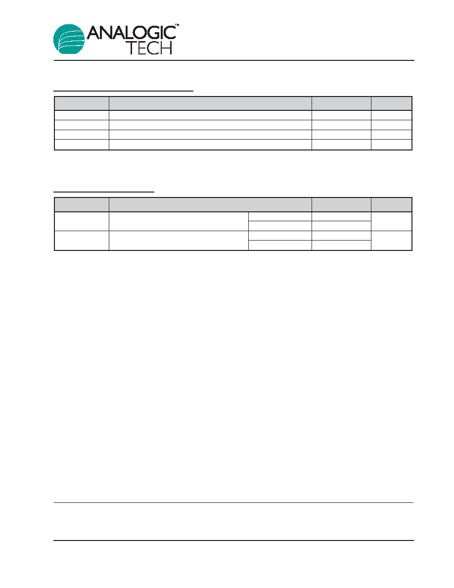
Absolute Maximum Ratings
1
Thermal Information
Symbol
Description
Value
Units
JA
Thermal Resistance
2
SC70JW-8
225
∞C/W
TSOPJW-12
160
P
D
Maximum Power Dissipation
3
SC70JW-8
440
mW
TSOPJW-12
625
Symbol
Description
Value
Units
V
CC
to GND
Input to GND
-0.3 to 6.0
V
OUTx to GND
Output (Source) to GND
-0.3 to V
IN
+ 0.3
V
EN/SET
EN/SET to GND
-0.3 to 6.0
V
T
J
Operating Junction Temperature Range
-40 to +150
∞C
AAT4296/98
Five/Six Channel Push/Pull I/O Expander
4296.2006.02.1.1
3
1. Stresses above those listed in Absolute Maximum Ratings may cause permanent damage to the device. Functional operation at condi-
tions other than the operating conditions specified is not implied. Only one Absolute Maximum Rating should be applied at any one time.
2. Mounted on an FR4 board.
3. Derate 4.4mW/∞C above 25∞C.
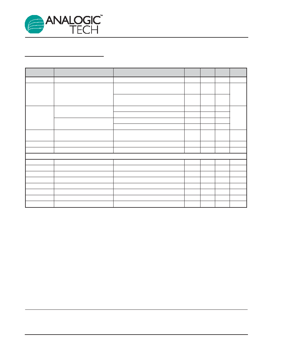
Electrical Characteristics
1
V
CC
= 5.0V; T
A
= -40∞C to +85∞C, unless otherwise noted. Typical values are T
A
= 25∞C.
Symbol
Description
Conditions
Min
Typ
Max
Units
V
CC
Supply Voltage Range
1.8
5.5
V
I
Q
Quiescent Current
EN/SET = V
CC
= 5V, I
OUT
= 0,
3.0
10
µA
All Switches ON
EN/SET = GND, V
CC
= 5V,
1.0
OUTx = Open
On Resistance P-Channel
V
CC
= 5V
2.5
6.0
R
DS(ON)
V
CC
= 3.6V
3.0
7.0
On Resistance N-Channel
V
CC
= 5V
1.9
6.0
V
CC
= 3.6V
2.0
7.0
T
CRDS
On Resistance
2800
ppm/∞C
Temperature Coefficient
T
ON
Output Turn-On Time
2
V
CC
= 5V, C
OUT
= 100nF; T
A
= 25∞C
1.6
2.7
µs
T
OFF
Output Turn-Off Time
3
V
CC
= 5V, C
OUT
= 100nF; T
A
= 25∞C
0.8
2.1
µs
EN/SET
V
EN(L)
Enable Threshold Low
V
IN
= 1.8V
0.4
V
V
EN(H)
Enable Threshold High
V
IN
= 5.5V
1.4
V
T
EN/SET LO
EN/SET Low Time
0.5
75
µs
T
EN/SET_HI_MIN
Minimum EN/SET High Time
50
ns
T
EN/SET_HI_MAX
Maximum EN/SET High Time
75
µs
T
OFF
EN/SET Off Timeout
500
µs
T
LAT
EN/SET Latch Timeout
500
µs
I
EN/SET
EN/SET Input Leakage
-1
1
µA
AAT4296/98
Five/Six Channel Push/Pull I/O Expander
4
4296.2006.02.1.1
1. The AAT4296/98 is guaranteed to meet performance specifications over the -40∞C to +85∞C operating temperature range and is
assured by design, characterization, and correlation with statistical process controls.
2. T
ON
is the time after latch timeout to 90% of the output voltage. See Figure 1.
3. T
OFF
is the time after off timeout to 10% of the output voltage. See Figure 1.

Typical Characteristics
Unless otherwise noted, V
IN
= 5V, C
IN
= 1µF, C
OUTx
= 0.1µF, T
A
= 25∞C.
P-Channel R
DS(ON)
vs. Temperature
(I
LOAD
= 100mA)
Temperature (
∞
∞C)
R
DS(ON)
(
)
R
DS3
R
DS1
1.7
1.9
2.1
2.3
2.5
2.7
2.9
3.1
3.3
-40
-20
0
20
40
60
80
100
R
DS6
R
DS5
R
DS4
R
DS2
P-Channel R
DS(ON)
vs. Input Voltage
(I
LOAD
= 100mA)
Input Voltage (V)
R
DS(ON)
(
)
0
5
10
15
20
25
1.5
2.0
2.5
3.0
3.5
4.0
4.5
5.0
5.5
R
DS1
R
DS2
R
DS6
R
DS5
R
DS4
R
DS3
V
IL
vs. Input Voltage
Input Voltage (V)
V
IL
(V)
0.4
0.5
0.6
0.7
0.8
0.9
1.0
1.5
2.0
2.5
3.0
3.5
4.0
4.5
5.0
5.5
85
∞
C
25
∞
C
-40
∞
C
V
IH
vs. Input Voltage
Input Voltage (V)
V
IH
(V)
0.6
0.7
0.8
0.9
1.0
1.1
1.2
1.5
2.0
2.5
3.0
3.5
4.0
4.5
5.0
5.5
85
∞
C
25
∞
C
-40
∞
C
Quiescent Current vs. Temperature
Temperature (
∞
∞C)
Quiescent Current (
µ
A)
1.0
1.5
2.0
2.5
3.0
3.5
4.0
4.5
5.0
-40
-20
0
20
40
60
80
100
V
IN
= 5.0V
V
IN
= 3.6V
Quiescent Current vs. Input Voltage
Input Voltage (V)
Quiescent Current (
µ
µ
A)
0.0
0.5
1.0
1.5
2.0
2.5
3.0
3.5
1.5
2
2.5
3
3.5
4
4.5
5
5.5
85∞C
25∞C
-40∞C
AAT4296/98
Five/Six Channel Push/Pull I/O Expander
4296.2006.02.1.1
5