 | –≠–ª–µ–∫—Ç—Ä–æ–Ω–Ω—ã–π –∫–æ–º–ø–æ–Ω–µ–Ω—Ç: AAT7126 | –°–∫–∞—á–∞—Ç—å:  PDF PDF  ZIP ZIP |
General Description
The AAT7126 30V N-Channel Power MOSFET is a
member of AnalogicTechTM's TrenchDMOSTM
product family. Using the ultra-high density propri-
etary TrenchDMOS technology, this product
demonstrates high power handling and small size.
Applications
∑
Battery-powered portable equipment
∑
Laptop computers
∑
Desktop computers
∑
DC/DC converters
Features
∑
V
DS(MAX)
= 30V
∑
I
D(MAX)
1
= 6.8A @ 25∞C
∑
Low R
DS(ON)
:
∑
26 m
@V
GS
= 10V
∑
41 m
@ V
GS
= 4.5V
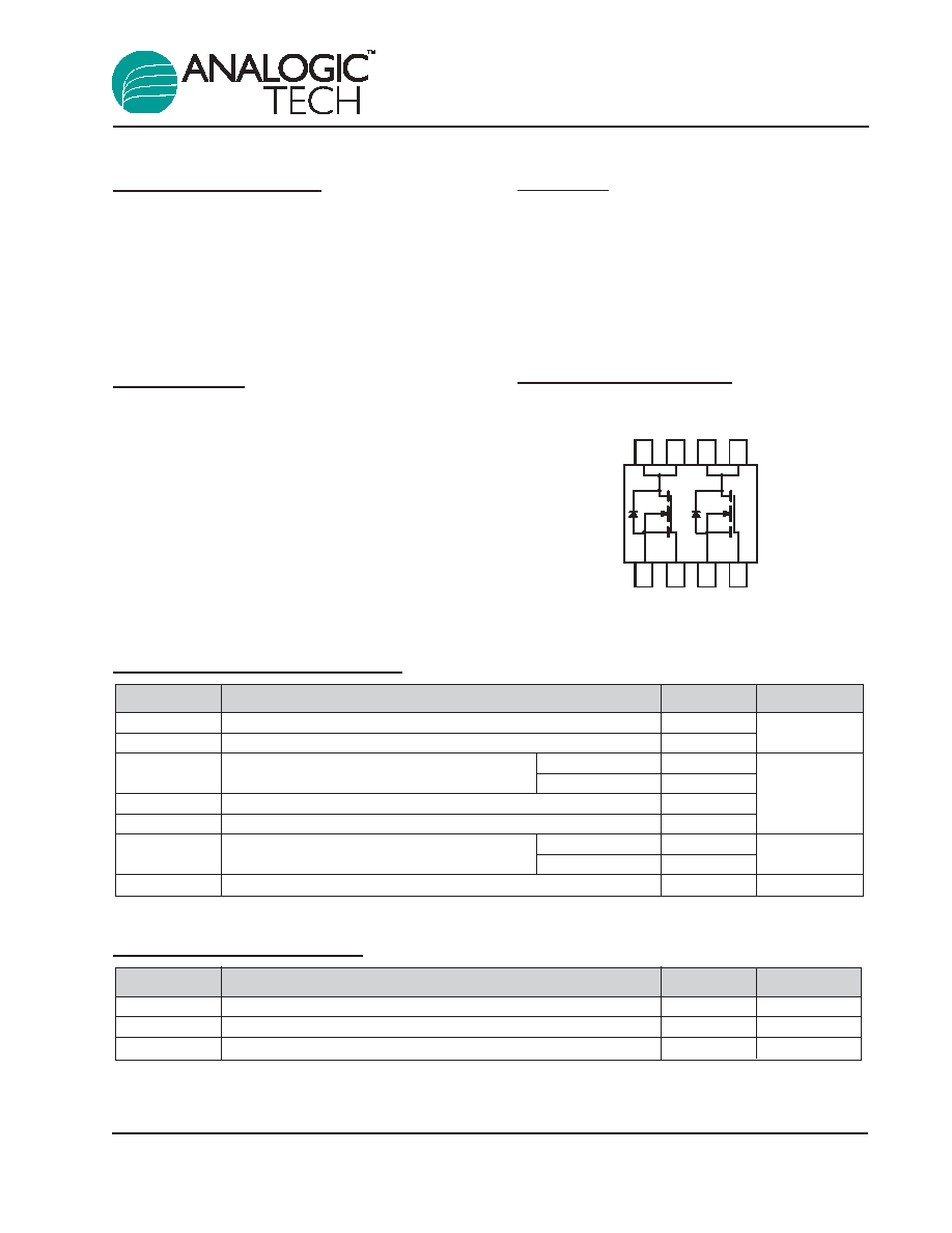
Dual SOP-8 Package
D1
D1
D2
D2
S1
G1
S2
G2
Top View
1
2
3
4
8
7
6
5
AAT7126
30V N-Channel Power MOSFET
Absolute Maximum Ratings
(T
A
=25∞C unless otherwise noted)
Thermal Characteristics
Symbol
Description
Value
Units
R
JA
Typical Junction-to-Ambient steady state, one FET on
100
∞C/W
R
JA2
Industry Standard Junction-to-Ambient Figure, t < 10 sec.
62.5
∞C/W
R
JC
Typical Junction-to-Case, one FET on
35
∞C/W
Symbol
Description
Value
Units
V
DS
Drain-Source Voltage
30
V
V
GS
Gate-Source Voltage
±20
I
D
Continuous Drain Current @ T
J
=150∞C
1
T
A
= 25∞C
±6.8
T
A
= 70∞C
±5.4
A
I
DM
Pulsed Drain Current
±24
I
S
Continuous Source Current (Source-Drain Diode)
1
1.7
P
D
Maximum Power Dissipation
1
T
A
= 25∞C
2.0
W
T
A
= 70∞C
1.25
T
J
, T
STG
Operating Junction and Storage Temperature Range
-55 to 150
∞C
Preliminary Information
7126.2002.10.0.9
1
Electrical Characteristics
(T
J
=25∞C unless otherwise noted)
Note 1: Mounted on 1" x 1" FR4 Copper Board, 10 sec pulse width.
Note 2: Pulse test: pulse width = 300µs
Note 3: Guaranteed by design. Not subjected to production testing.
Symbol
Description
Conditions
Min
Typ
Max
Units
DC Characteristics
BV
DSS
Drain-Source Breakdown Voltage V
GS
=0V, I
D
=250µA
30
V
R
DS(ON)
Drain-Source ON-Resistance
2
V
GS
=10V, I
D
=6.8A
19.5
26
m
V
GS
=4.5V, I
D
=5.4A
32
41
I
D(ON)
On-State Drain Current
2
V
GS
=10V ,V
DS
=5V (Pulsed)
24
A
V
GS(th)
Gate Threshold Voltage
V
GS
=V
DS
, I
D
=250µA
1.0
V
I
GSS
Gate-Body Leakage Current
V
GS
=±20V, V
DS
=0V
±100
nA
I
DSS
Drain Source Leakage Current
V
GS
=0V,V
DS
=30V
1
µA
V
GS
=0V,V
DS
=30V, T
J
=70∞C
5
g
fs
Forward Transconductance
2
V
DS
=5V, I
D
=6.8A
14
S
Dynamic Characteristics
3
Q
G
Total Gate Charge
V
DS
=15V, I
D
=6.8A, V
GS
=5V
8.6
13
nC
Q
GT
Total Gate Charge
V
DS
=15V, I
D
=6.8A, V
GS
=10V
16
24
nC
Q
GS
Gate-Source Charge
V
DS
=15V, I
D
=6.8A, V
GS
=10V
2.5
nC
Q
GD
Gate-Drain Charge
V
DS
=15V, I
D
=6.8A, V
GS
=10V
2.8
nC
t
D(ON)
Turn-ON Delay
V
DD
=15V, V
GS
=10V, R
D
=3
, R
G
=6
3
ns
t
R
Turn-ON Rise Time
V
DD
=15V, V
GS
=10V, R
D
=3
, R
G
=6
3
ns
t
D(OFF)
Turn-OFF Delay
V
DD
=15V, V
GS
=10V, R
D
=3
, R
G
=6
12
ns
t
F
Turn-OFF Fall Time
V
DD
=15V, V
GS
=10V, R
D
=3
, R
G
=6
6
ns
Source-Drain Diode Characteristics
V
SD
Source-Drain Forward Voltage
2
V
GS
=0, I
S
=1.7A
1.2
V
I
S
Continuous Diode Current
1.7
A
AAT7126
30V N-Channel Power MOSFET
2
7126.2002.10.0.9
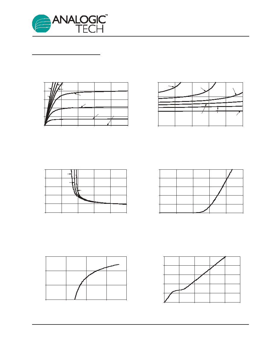
Typical Characteristics
(T
J
= 25∫C unless otherwise noted)
Gate Charge Characteristics
0
2
4
6
8
10
0
4
8
12
16
20
Gate Charge (nC)
Gate Voltage (V)
Source to Drain Voltage
0.1
1
10
100
0.4
0.6
0.8
1
1.2
V
SD
(V)
I
SD
(A)
Transfer
0
5
10
15
20
25
0
1
2
3
4
5
V
G
(V)
I
D
(A)
R
DS(ON)
vs. V
G
0
20
40
60
80
100
0
2
4
6
8
10
V
G
(V)
R
DS(ON)
(m
)
5A
10A
15A
Normalized R
DS(ON)
0
1
2
3
0
5
10
15
20
25
I
D
(A)
R
DS(ON)
/ R
DS(ON)
at gate = 10 V
3.5V
4V
4.5V
5V
6V
10V
Forward Characteristics
0
5
10
15
20
25
0
1
2
3
4
5
V
D
(V)
I
D
(A)
10V
6V
5V
4V
3.5V
4.5V
3V
2V
AAT7126
30V N-Channel Power MOSFET
7126.2002.10.0.9
3
Ordering Information
Note: Sample stock is generally held on all part numbers listed in BOLD.
Package Information
SOP-8
All dimensions in millimeters.
0.175
±
0.075
6.00
±
0.20
3.90
±
0.10
1.55
±
0.20
1.27 BSC
0.42
± 0.09 ◊ 8
4.90
± 0.10
4
∞
±
4
∞
45
∞
0.375
± 0.125
0.235
± 0.045
0.825
± 0.445
Package
Marking
Part Number (Tape and Reel)
SOP-8
7126
AAT7126IAS-T1
AAT7126
30V N-Channel Power MOSFET
4
7126.2002.10.0.9
Advanced Analogic Technologies, Inc.
830 E. Arques Avenue, Sunnyvale, CA 94085
Phone (408) 737-4600
Fax (408) 737-4611
AnalogicTech cannot assume responsibility for use of any circuitry other than circuitry entirely embodied in an AnalogicTech product. No circuit patent licenses, copyrights, mask work
rights, or other intellectual property rights are implied.
AnalogicTech reserves the right to make changes to their products or specifications or to discontinue any product or service without notice, and advise customers to obtain the latest
version of relevant information to verify, before placing orders, that information being relied on is current and complete. All products are sold subject to the terms and conditions of sale
supplied at the time of order acknowledgement, including those pertaining to warranty, patent infringement, and limitation of liability.
AnalogicTech warrants performance of its semiconductor products to the specifications applicable at the time of sale in accordance with AnalogicTech's standard warranty. Testing and
other quality control techniques are utilized to the extent AnalogicTech deems necessary to support this warranty. Specific testing of all parameters of each device is not necessarily
performed.