General Description
The AAT7357 is a low threshold dual MOSFET
designed for the battery, cell phone, and PDA mar-
kets. Using AnalogicTechTM's ultra high density
MOSFET process and space saving small outline J-
lead package, performance superior to that normal-
ly found in a TSSOP-8 footprint has been squeezed
into the footprint of a TSOPJW-8 package.
Applications
∑
Battery Packs
∑
Cellular & Cordless Telephones
∑
Battery-powered portable equipment
Features
∑
V
DS(MAX)
= -20V
∑
I
D(MAX)
1
= -5A @ 25įC
∑
Low R
DS(ON)
:
∑
39 m
@ V
GS
= -4.5V
∑
63 m
@ V
GS
= -2.5V
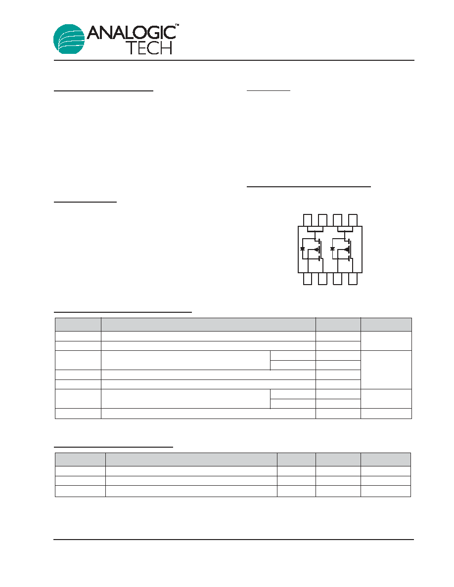
Dual TSOPJW-8 Package
D1
D1
D2
D2
S1
G1
S2
G2
Top View
1
2
3
4
8
7
6
5
AAT7357
20V P-Channel Power MOSFET
Absolute Maximum Ratings
(T
A
=25įC unless otherwise noted)
Thermal Characteristics
Symbol
Description
Typ
Max
Units
R
JA
Junction-to-Ambient steady state, one FET on
1
115
140
įC/W
R
JA2
Junction-to-Ambient t<5 seconds
1
64
78
įC/W
R
JF
Junction-to-Foot
1
60
72
įC/W
Symbol
Description
Value
Units
V
DS
Drain-Source Voltage
-20
V
V
GS
Gate-Source Voltage
Ī12
I
D
Continuous Drain Current @ T
J
=150įC
1
T
A
= 25įC
Ī5
T
A
= 70įC
Ī4
A
I
DM
Pulsed Drain Current
2
Ī12
I
S
Continuous Source Current (Source-Drain Diode)
1
-1.3
P
D
Maximum Power Dissipation
1
T
A
= 25įC
1.6
W
T
A
= 70įC
1.0
T
J
, T
STG
Operating Junction and Storage Temperature Range
-55 to 150
įC
Advanced Information
7357.2003.08.0.6
1
Electrical Characteristics
(T
J
=25įC unless otherwise noted)
Notes:
1. Based on thermal dissipation from junction to ambient while mounted on a 1" x 1" PCB with optimized layout. A 5 second pulse on a
1" x 1" PCB approximates testing a device mounted on a large multi-layer PCB as in most applications. R
JF
+ R
FA
= R
JA
where the
foot thermal reference is defined as the normal solder mounting surface of the device's leads. R
JF
is guaranteed by design, however
R
CA
is determined by the PCB design. Actual maximum continuous current is limited by the application's design.
2. Pulse test: Pulse Width = 300 Ķs
3. Guaranteed by design. Not subject to production testing.
Symbol
Description
Conditions
Min
Typ Max
Units
DC Characteristics
BV
DSS
Drain-Source Breakdown Voltage V
GS
=0V, I
D
=-250ĶA
-20
V
R
DS(ON)
Drain-Source ON-Resistance
2
V
GS
=-4.5V, I
D
=-5A
30
39
m
V
GS
=-2.5V, I
D
=-4A
49
63
I
D(ON)
On-State Drain Current
2
V
GS
=-4.5V, V
DS
=-5V (Pulsed)
-12
A
V
GS(th)
Gate Threshold Voltage
V
GS
=V
DS
, I
D
=-250ĶA
-0.6
V
I
GSS
Gate-Body Leakage Current
V
GS
=Ī12V, V
DS
=0V
Ī100
nA
I
DSS
Drain Source Leakage Current
V
GS
=0V, V
DS
=-20V
-1
ĶA
V
GS
=0V, V
DS
=-16V, T
J
=70įC
3
-5
g
fs
Forward Transconductance
2
V
DS
=-5V, I
D
=-5A
12
S
Dynamic Characteristics
3
Q
G
Total Gate Charge
V
DS
=-10V, R
D
=2.0
, V
GS
=-4.5V
14
Q
GS
Gate-Source Charge
V
DS
=-10V, R
D
=2.0
, V
GS
=-4.5V
3.5
nC
Q
GD
Gate-Drain Charge
V
DS
=-10V, R
D
=2.0
, V
GS
=-4.5V
5.6
t
D(ON)
Turn-ON Delay
V
DS
=-10V, R
D
=2.0
, V
GS
=-4.5V, R
G
=6
TBD
t
R
Turn-ON Rise Time
V
DS
=-10V, R
D
=2.0
, V
GS
=-4.5V, R
G
=6
TBD
ns
t
D(OFF)
Turn-OFF Delay
V
DS
=-10V, R
D
=2.0
, V
GS
=-4.5V, R
G
=6
TBD
t
F
Turn-OFF Fall Time
V
DS
=-10V, R
D
=2.0
, V
GS
=-4.5V, R
G
=6
TBD
Source-Drain Diode Characteristics
V
SD
Source-Drain Forward Voltage
2
V
GS
=0, I
S
=-5A
-1.2
V
I
S
Continuous Diode Current
1
-1.3
A
AAT7357
20V P-Channel Power MOSFET
2
7357.2003.08.0.6
Typical Characteristics
(T
J
= 25ļC unless otherwise noted)
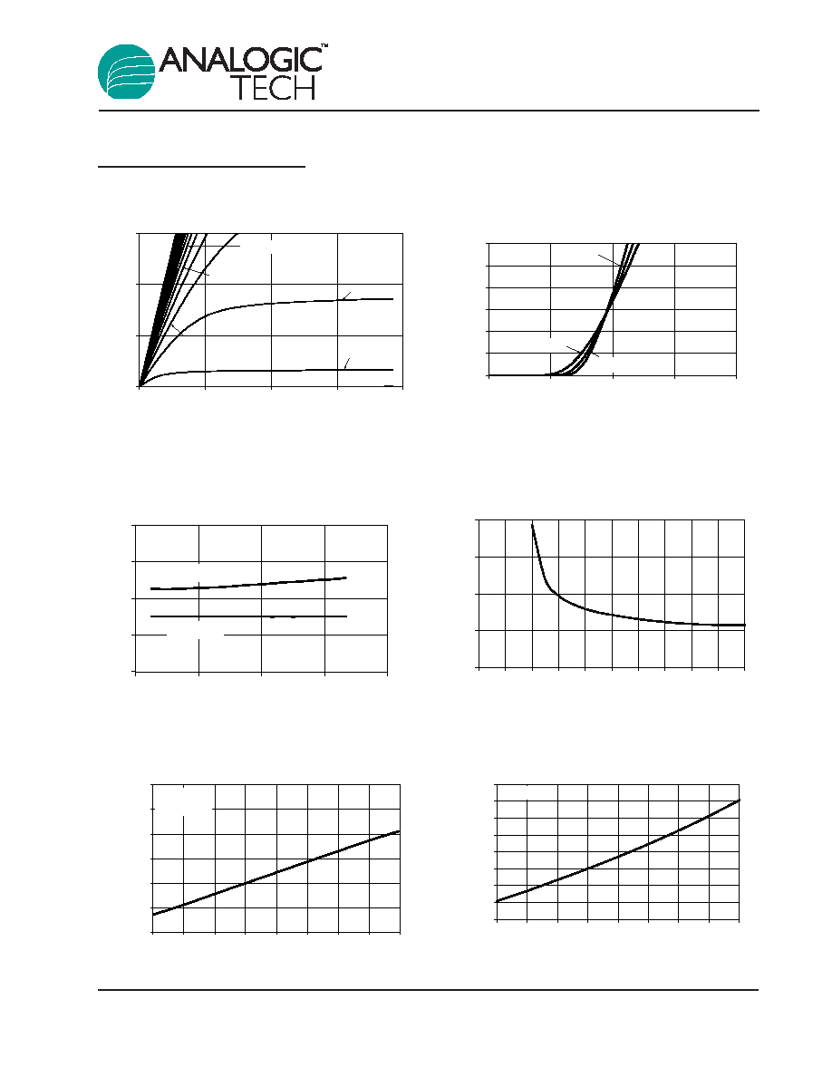
Threshold Voltage
T
J
(
įC)
V
GS(th)
Variance (V)
-0.3
-0.2
-0.1
0
0.1
0.2
0.3
0.4
0.5
-50
-25
0
25
50
75
100
125
150
I
D
= 250
ĶA
On-Resistance vs. Junction Temperature
T
J
(
įC)
Normalized R
DS(ON)
0.6
0.8
1.0
1.2
1.4
1.6
1.8
-50
-25
0
25
50
75
100
125
150
V
GS
= 4.5V
I
D
= 4.5A
On-Resistance vs. Gate to Source Voltage
V
GS
(V)
R
DS(ON)
(m
)
0
0.02
0.04
0.06
0.08
0
1
2
3
4
5
6
7
8
9
10
On-Resistance vs. Drain Current
I
D
(A)
R
DS(ON)
(
)
0
0.02
0.04
0.06
0.08
0
5
10
15
20
V
GS
= 2.5 V
V
GS
= 4.5 V
Transfer Characteristics
V
GS
(V)
I
D
(A)
0
2
4
6
8
10
12
0
1
2
3
4
V
D
= V
G
25
įC
-55
įC
125
įC
Output Characteristics
V
DS
(V)
I
DS
(A)
1.5V
2.5V
3V
2V
3.5V
0
4
8
12
0
0.5
1
1.5
2
4V through 10V
AAT7357
20V P-Channel Power MOSFET
7357.2003.08.0.6
3
Typical Characteristics
(T
J
= 25ļC unless otherwise noted)
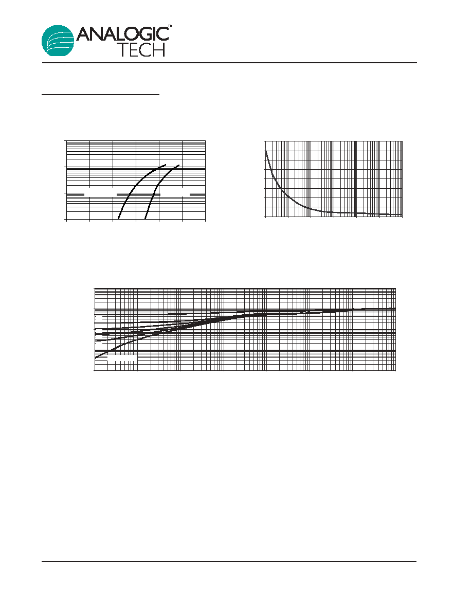
Transient Thermal Response, Junction to Ambient
Time (s)
Normalized Effective
Transient Thermal Impedance
0.001
0.01
0.1
1
10
0.0001
0.001
0.01
0.1
1
10
100
1000
Single Pulse
.5
.2
.1
.01
.02
Single Pulse Power, Junction to Ambient
Time (s)
Power (W)
0
5
10
15
20
25
30
35
40
1.00E-03 1.00E-02 1.00E-01 1.00E+01 1.00E+01 1.00E+02 1.00E+03
Source-Drain Diode Forward Voltage
V
SD
(V)
I
S
(A)
0.1
1
10
100
0
0 .2
0.4
0 .6
0.8
1
1.2
T
J
= 150
įC
T
J
= 25
įC
AAT7357
20V P-Channel Power MOSFET
4
7357.2003.08.0.6
Ordering Information
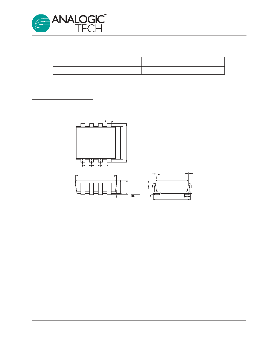
Package Information
TSOPJW-8
All dimensions in millimeters.
0.65 BSC 0.65 BSC 0.65 BSC
0.325
Ī
0.075
2.85
Ī
0.20
2.40
Ī
0.10
3.025
Ī
0.075
0.055
Ī
0.045
0.9625
Ī
0.0375
1.0175
Ī
0.0925
0.010
0.15
Ī
0.05
7
į
0.04 REF
0.45
Ī
0.15
2.75
Ī
0.25
Package
Marking
Part Number (Tape and Reel)
TSOPJW-8
AAT7357ITS-T1
AAT7357
20V P-Channel Power MOSFET
7357.2003.08.0.6
5

AAT7357
20V P-Channel Power MOSFET
6
7357.2003.08.0.6
Advanced Analogic Technologies, Inc.
830 E. Arques Avenue, Sunnyvale, CA 94085
Phone (408) 737-4600
Fax (408) 737-4611
AnalogicTech cannot assume responsibility for use of any circuitry other than circuitry entirely embodied in an AnalogicTech product. No circuit patent licenses, copyrights, mask work
rights, or other intellectual property rights are implied.
AnalogicTech reserves the right to make changes to their products or specifications or to discontinue any product or service without notice, and advise customers to obtain the latest
version of relevant information to verify, before placing orders, that information being relied on is current and complete. All products are sold subject to the terms and conditions of sale
supplied at the time of order acknowledgement, including those pertaining to warranty, patent infringement, and limitation of liability.
AnalogicTech warrants performance of its semiconductor products to the specifications applicable at the time of sale in accordance with AnalogicTech's standard warranty. Testing and
other quality control techniques are utilized to the extent AnalogicTech deems necessary to support this warranty. Specific testing of all parameters of each device is not necessarily
performed.