AAT9055
30V N-Channel Power MOSFET
Preliminary Information
9055.2003.04.0.61
1
PWMSwitch
TM
General Description
The AAT9055 30 V N-Channel Power MOSFET is a
member of AnalogicTechTM's TrenchDMOSTM prod-
uct family. Using the ultra-high density proprietary
TrenchDMOS technology, this product demon-
strates high power handling and small size.
Applications
∑
DC-DC converters
∑
High current load switches
∑
LDO output
Features
∑
V
DS(MAX)
= 30V
∑
I
D(MAX)
1
= 12 A @ T
C
= 25∞C
∑
I
APP(MAX)
= 6A in typical computer application
∑
Low R
DS(ON)
:
∑
56 m
@V
GS
= 10V
∑
90 m
@V
GS
= 4.5V
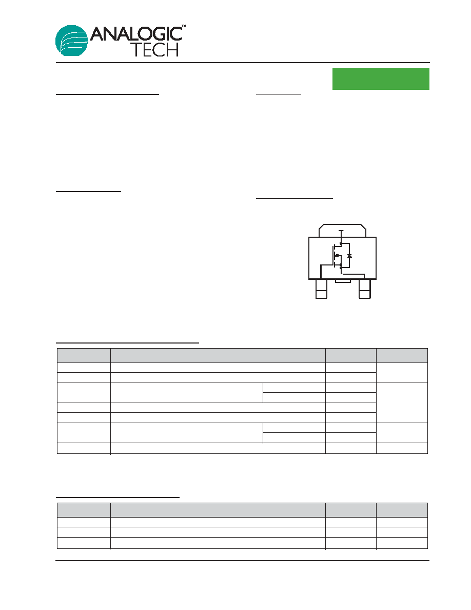
DPAK Package
G
S
Drain-Connected Tab
Absolute Maximum Ratings
(T
C
=25∞C unless otherwise noted)
Thermal Characteristics
Symbol
Description
Value
Units
R
JA
Maximum Junction-to-Ambient
100
∞C/W
R
TYP
Typical Junction to ambient on PC board
2
28
∞C/W
R
JC
Maximum Junction-to-Case
5.5
∞C/W
Symbol
Description
Value
Units
V
DS
Drain-Source Voltage
30
V
V
GS
Gate-Source Voltage
±20
I
D
Continuous Drain Current @ T
J
=150∞C
1
T
C
= 25∞C
±12
T
C
= 70∞C
±10
I
DM
Pulsed Drain Current
3
±16
A
I
S
Continuous Source Current (Source-Drain Diode)
1
12
P
D
Maximum Power Dissipation
1
T
C
= 25∞C
22
W
T
C
= 70∞C
14
T
J
, T
STG
Operating Junction and Storage Temperature Range
-55 to 150
∞C
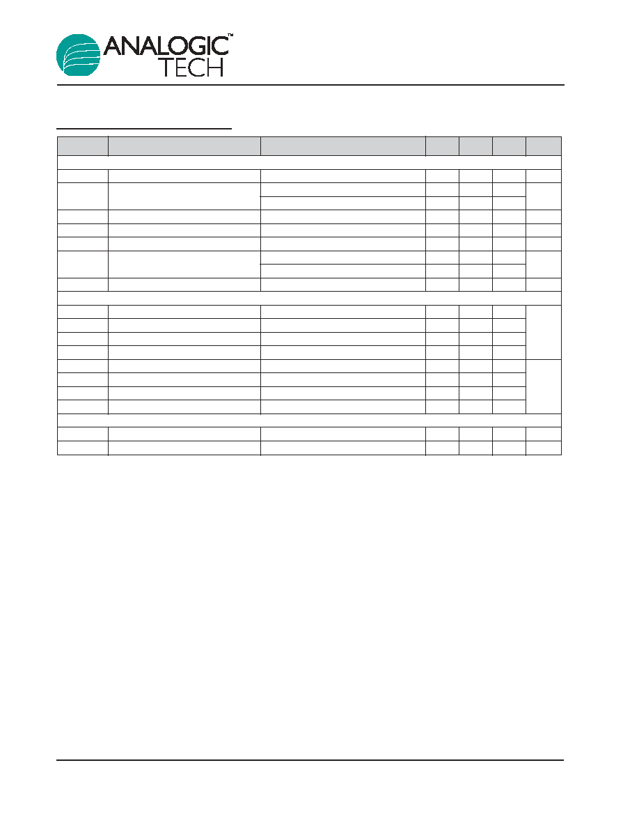
Electrical Characteristics
(T
J
=25∞C unless otherwise noted)
Notes:
1. Based on thermal dissipation from junction to case. R
JC
+ R
CA
= R
JA
where the case thermal reference is defined as the solder
mounting surface of the drain tab. R
JC
is guaranteed by design, however R
CA
is determined by the PCB design. Package current is
limited to 8A DC and 16A pulsed.
2. Mounted on typical computer main board.
3. Pulse measurement 300 µs.
4. Guaranteed by design. Not subject to production testing.
Symbol Description
Conditions
Min
Typ
Max
Units
DC Characteristics
BV
DSS
Drain-Source Breakdown Voltage
V
GS
=0V, I
D
=250µA
30
V
R
DS(ON)
Drain-Source ON-Resistance
3
V
GS
=10V, I
D
=12A
44
56
m
V
GS
=4.5V, I
D
=10A
68
90
I
D(ON)
On-State Drain Current
3
V
GS
=10V, V
DS
=5V (Pulsed)
16
A
V
GS(th)
Gate Threshold Voltage
V
GS
=V
DS
, I
D
=250µA
1.0
V
I
GSS
Gate-Body Leakage Current
V
GS
=±20V, V
DS
=0V
±100
nA
I
DSS
Drain Source Leakage Current
V
GS
=0V,V
DS
=30V
1
µA
V
GS
=0V,V
DS
=30V, T
J
=70∞C
25
g
fs
Forward Transconductance
3
V
DS
=5V, I
D
=4A
6
S
Dynamic Characteristics
4
Q
G
Total Gate Charge
V
DS
=15V, R
D
=2.5
, V
GS
=5V
4.2
Q
GT
Total Gate Charge
V
DS
=15V, R
D
=2.5
, V
GS
=10V
7.7
Q
GS
Gate-Source Charge
V
DS
=15V, R
D
=2.5
, V
GS
=10V
1.35
nC
Q
GD
Gate-Drain Charge
V
DS
=15V, R
D
=2.5
, V
GS
=10V
1.2
t
D(ON)
Turn-ON Delay
V
DD
=15V, R
D
=2.5
, V
GS
=10V, R
G
=6
2.5
t
R
Turn-ON Rise Time
V
DD
=15V, R
D
=2.5
, V
GS
=10V, R
G
=6
2.6
t
D(OFF)
Turn-OFF Delay
V
DD
=15V, R
D
=2.5
, V
GS
=10V, R
G
=6
12
ns
t
F
Turn-OFF Fall Time
V
DD
=15V, R
D
=2.5
, V
GS
=10V, R
G
=6
5.7
Source-Drain Diode Characteristics
V
SD
Source-Drain Forward Voltage
3
V
GS
=0, I
S
=12A
1.2
1.5
V
I
S
Continuous Diode Current
1
12
A
AAT9055
30V N-Channel Power MOSFET
2
9055.2003.04.0.61
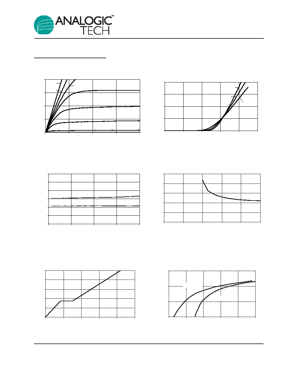
Typical Characteristics
Source-Drain Diode Forward Voltage
0.1
1
10
100
0.4
0.6
0.8
1
1.2
1.4
V
I
S
(A)
SD
(V)
T
J
= 25
∞C
T
J
= 150
∞C
Gate Charge
0
2
4
6
8
10
0
2
4
6
8
10
Q
G
, Charge (nC)
V
GS
(V)
V
D
=15V
R
D
=2.5
On-Resistance vs. Gate to Source Voltage
0
20
40
60
80
100
0
2
4
6
8
10
V
GS
(V)
R
DS(ON)
(m
)
I
D
= 10A
On-Resistance vs. Drain Current
I
D
(A)
R
DS(ON)
(m
)
0
20
40
60
80
100
120
0
4
8
12
16
V
GS
= 4.5V
V
GS
= 10V
Transfer Characteristics
V
GS
(V)
I
D
(A)
0
4
8
12
16
0
1
2
3
4
5
V
D
=V
G
25∞C
-55∞C
125∞C
Output Characteristics
V
DS
(V)
I
DS
(A)
2V
0
4
8
12
16
0
1
2
3
4
3V
6V
3.5V
5V
4.5V
10V
4V
AAT9055
30V N-Channel Power MOSFET
9055.2003.04.0.61
3
Ordering Information
Note: Sample stock is generally held on all part numbers listed in BOLD.
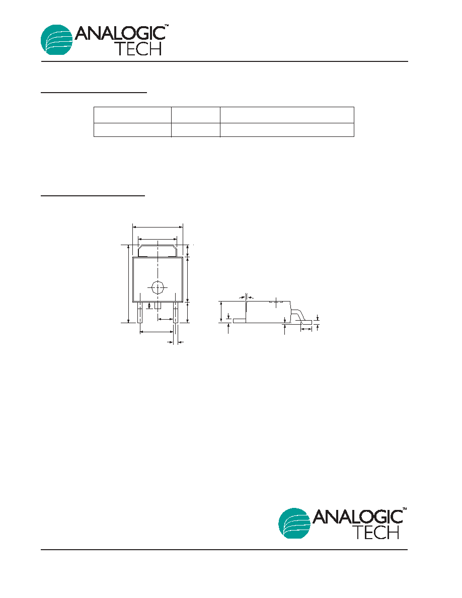
Package Information
TO-252 (DPAK)
All measurements in millimeters.
2.29 BSC
7.5
∞ ± 7.5∞
5.205
± 0.255
1.145
0.58
± 0.13
1.59
± 0.19
5.775
±
0.445
1.46
±
0.57
6.54
± 0.19
2.67 REF
2.285
±
0.105
0.83
±
0.19
0.72
± 0.17
9.855
±
0.555
0.50
0.13
Package
Marking
Part Number (Tape and Reel)
TO-252 (DPAK)
9055
AAT9055INY-T1
AAT9055
30V N-Channel Power MOSFET
4
9055.2003.04.0.61
Advanced Analogic Technologies, Inc.
830 E. Arques Avenue, Sunnyvale, CA 94085
Phone (408) 737-4600
Fax (408) 737-4611
AnalogicTech cannot assume responsibility for use of any circuitry other than circuitry entirely embodied in an AnalogicTech product. No circuit patent licenses, copyrights, mask work
rights, or other intellectual property rights are implied.
AnalogicTech reserves the right to make changes to their products or specifications or to discontinue any product or service without notice, and advise customers to obtain the latest
version of relevant information to verify, before placing orders, that information being relied on is current and complete. All products are sold subject to the terms and conditions of sale
supplied at the time of order acknowledgement, including those pertaining to warranty, patent infringement, and limitation of liability.
AnalogicTech warrants performance of its semiconductor products to the specifications applicable at the time of sale in accordance with AnalogicTech's standard warranty. Testing and
other quality control techniques are utilized to the extent AnalogicTech deems necessary to support this warranty. Specific testing of all parameters of each device is not necessarily
performed.