Available on Tape
and Reel For Pick and
Place Manufacturing.
USA/Canada:
Toll Free:
Europe
:
(315) 432-8909
(800) 544-2414
+44 2392-232392
Model 1P603
Rev. A
Hybrid Couplers
3 dB, 90
�
Description
The 1P603 Pico Xinger is a low profile, miniature 3dB hybrid coupler in an
easy to use surface mount package designed for W-LAN and MMDS
applications. The 1P603 is designed for balanced amplifiers, variable
phase shifters and attenuators, LNAs, signal distribution and is an ideal
solution for the ever-increasing demands of the wireless industry for smaller
printed circuit boards and high performance. Parts have been subjected to
rigorous qualification testing and units are 100% tested. They are
manufactured using materials with x and y thermal expansion coefficients
compatible with common substrates.
ELECTRICAL
SPECIFICATIONS**
Frequency
Isolation
Insertion
Loss
VSWR
GHz
dB Min
dB Max
Max:1
2.3 � 2.7
20
0.30
1.20
Amplitude
Balance
Phase
Balance
Power
JC
Operating
Temp.
dB Max
Degrees
Ave. CW Watts
�C/Watt
�C
Features:
� 2.3 � 2.7 GHz.
� W-LAN and MMDS
� Low Loss
� High Isolation
� 90o Quadrature
� Surface Mountable
� Tape And Reel
� New Pico-Package
� 100% Tested
� 0.25
� 3
25
30.6
-55 to +85
**Specification based on performance of unit properly installed on microstrip printed circuit
boards with 50
nominal impedance. Specifications subject to change without notice.
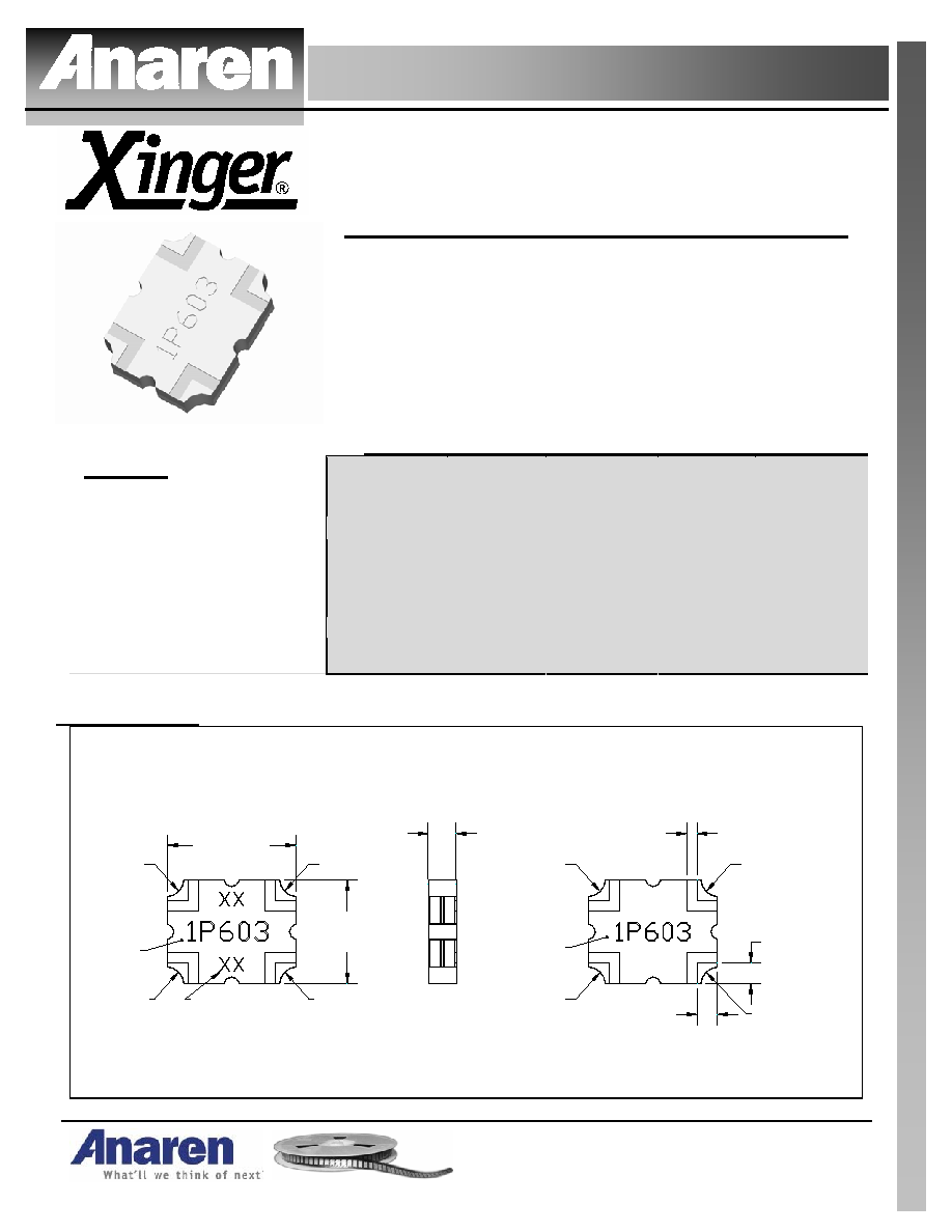
Outline Drawing
1P603 Rev A Mechanical Outline
Dimensions are in Inches [Millimeters]
.054
�.005
[1.38
�0.13
]
Top View (Near-side)
Bottom View (Far-side)
Pin 1
Pin 4
Pin 3
Pin 2
GND
Side View
.250
�.010
[6.35
�0.25
]
.200
�.010
[5.08
�0.25
]
Pin 1
Pin 2
Pin 4
Pin 3
GND
Denotes Array
Number
.040
�.008
[1.01
�0.20
]
.040
�.008
[1.01
�0.20
]
.020
�.004
TYP
[0.51
�0.10
]
Part Is Symmetric About All Axis
USA/Canada:
Toll Free:
Europe:
(315) 432-8909
(800) 544-2414
+44 2392-232392
Available on Tape and
Reel For Pick and Place
Manufacturing.
Model 1P603
Rev. A
Typical Performance: 2.2 GHz. to 2.8 GHz.
Coupling 1P603
-3.8
-3.5
-3.2
-2.9
-2.6
2200
2300
2400
2500
2600
2700
2800
Frequency (MHz)
C
oupl
i
n
g (
d
B
)
Return Loss 1P603
-50
-40
-30
-20
-10
0
2200
2300
2400
2500
2600
2700
2800
Frequency (MHz)
R
e
t
u
rn
L
o
s
s
(d
B
)
Isolation 1P603
-50
-40
-30
-20
-10
2200
2300
2400
2500
2600
2700
2800
Frequency (MHz)
I
s
o
l
at
i
o
n (
d
B
)
Phase Balance 1P603
-93
-92
-91
-90
-89
-88
-87
2200
2300
2400
2500
2600
2700
2800
Frequency (MHz)
P
h
a
s
e B
a
l
a
n
c
e (D
eg
re
es
)
AMPLITUDE BALANCE
3dB hybrids are a type of backward wave coupler. In the
design of these couplers, the even mode impedance was
chosen to `critically couple' or slightly `over couple' at mid
band to maximize performance and bandwidth. The
amplitude balance specification is defined as the
difference (in dB) of the signals at the COUPLED port
output and the DC port output, when compared to the
average output level.
PHASE BALANCE
In theory, output ports of a backward wave hybrid coupler
remain in perfect phase quadrature independent of
frequency. In practice, factors associated with the
manufacturing processes slightly degrade performance.
The specification is typical two to three degrees maximum
although in practice, phase balance is statistically better
than specified (<1
o
).
VSWR & ISOLATION
Similar to phase balance, the VSWR and isolation of a
coupler are theoretically perfect; where the input and
output ports are perfectly matched and no power is
coupled to the isolated port. In practice, factors
associated with the design and manufacturing
processes limit VSWR and isolation. The significant
limitations are associated with limitations of building
perfect 50
transitions at the input and output ports of
the device.
INSERTION LOSS
Coupler insertion loss is defined as the difference of the
input power from the sum of the output power. In
practice, loss is typically 0.20 dB. Specification limits
are somewhat higher due to imperfect test conditions;
USA/Canada:
Toll Free:
Europe:
(315) 432-8909
(800) 544-2414
+44 2392-232392
Available on Tape and
Reel For Pick and Place
Manufacturing.
Model 1P603
Rev. A
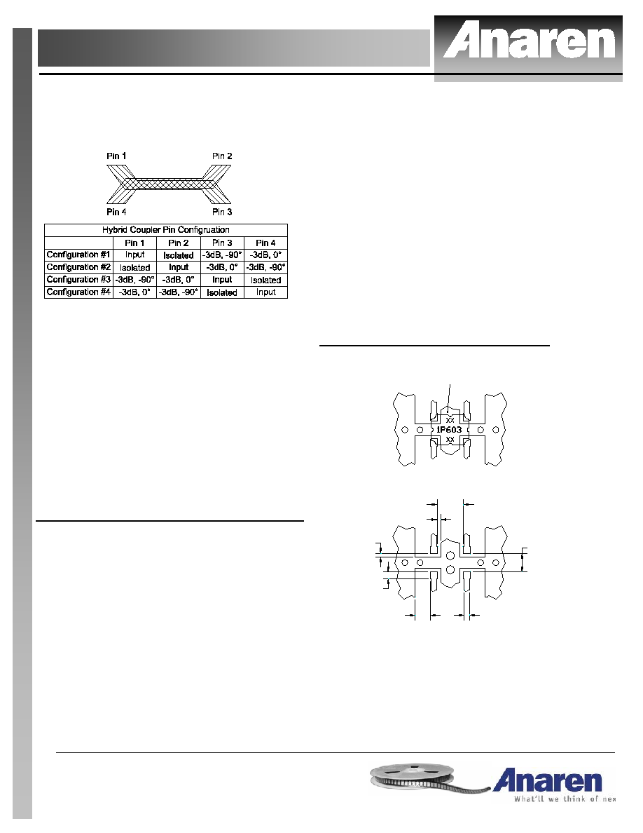
PIN CONFIGURATION
All of the standard surface mount 3dB hybrid couplers
have pin orientations that are symmetrical. When a port
is designated as the input, automatically the two output
and isolated ports are defined. For example, if the input
port for a device was selected to be Pin 1, Pin 2 is
automatically the isolated port, Pin 4 is the 0 degree
reference output port, and Pin 3 is the output port which
"lags" behind the reference output port by 90 degrees.
Similarly, if Pin 3 was to be selected as the input port,
the adjacent port on the long side (Pin 4) is the isolated
port, the adjacent port on the short side (Pin 2) is the 0
degree output port, and the opposite port (Pin 1) is the -
90 degree output port. Below is a table of all possible
orientations.
MOUNTING
In order for Xinger surface mount couplers to work
optimally, there must be 50
transmission lines leading
to and from all of the RF ports. Also, there must be a
very good ground plane under the part to ensure proper
electrical performance. If either of these two conditions
are not satisfied, insertion loss, coupling, VSWR and
isolation may not meet published specifications.
Overall ground is improved if a dense population of
plated through holes connect the top and bottom ground
layers of the PCB. This minimizes ground inductance
and improves ground continuity. All of the Xinger hybrid
and directional couplers are constructed from ceramic
filled PTFE composites which possess excellent
electrical and mechanical stability having X and Y
thermal coefficient of expansion (CTE) of 17 ppm/
o
C
When a surface mount hybrid coupler is mounted to a
printed circuit board, the primary concerns are;
insuring the RF pads of the device are in contact with
the circuit trace of the PCB and insuring the ground
plane of neither the component nor the PCB is in
contact with the RF signal. As long as the geometry
of the unit fits onto the layout of the circuit trace on
the PCB, and the conditions of the previous
paragraph are followed, the coupler's performance is
ensured. An example of how the PCB footprint could
look is shown below. In specific designs, the 50
lines need to be adjusted to the unique dielectric
coefficients and thicknesses as well as varying pick
and place equipment tolerances.
SUGGESTED FOOTPRINT
1P603 Rev A Mounting Footprint
Dimensions are in Inches [Millimeters]
Part Is Symmetric About All Axis
.174
[4.42]
.124
[3.15]
4X 50
Transmission
Line
To ensure proper electrical and thermal performance
there must be a ground plane with 100%
solder conection underneath the part
4X .045 SQ
[1.14]
4X .024
[0.61]
4X .099
[2.51]
4X .024 [0.61]