
Available on Tape
and Reel For Pick and
Place Manufacturing.
USA/Canada:
Toll Free:
Europe
:
(315) 432-8909
(800) 544-2414
+44 2392-232392
Model JA1305-5
Rev. A
Directional Couplers
5 dB
Description
The JA1305-5 is a low profile 5dB directional coupler in an easy to use
surface mount package covering WCDMA and other 3G applications. The
JA1305-5 is ideal for 3 way inline splitting and combining amplifiers and for
power injection. The coupler can be used in most high power designs.
Parts have been subjected to rigorous qualification testing and units are
100% tested. They are manufactured using materials with x and y thermal
expansion coefficients compatible with common substrates such as FR4,
G-10 and polyamide.
ELECTRICAL
SPECIFICATIONS**
Frequency
Mean
Coupling
Insertion
Loss
VSWR
Freq.
Sensitivity
GHz
dB
dB Max
Max:1
dB Max
2.11 � 2.17
5.0 � 0.25
0.23
1.20
�0.10
2.0 � 2.3
5.1 � 0.4
0.25
1.25
�0.20
Deviation from
Linear Phase (50
MHz. Band)
Directivity
Power
Handling
JC
Operating
Temp.
Deg. Max
dB Min
Watts
�C / Watt
�C
NA
20
55
15.35
-55 to +85
Features:
� 2.0 - 2.3 GHz
� Optimized for 3G
� Low Insertion loss
� High Directivity
� Surface Mountable
� Tape And Reel
� Convenient Package
� 100% Tested
�0.10
18
50
15.35
-55 to +85
**Specification based on performance of unit properly installed on microstrip printed circuit
boards with 50
nominal impedance. Specifications subject to change without notice.
Outline Drawing
JA1305-5 Rev A Mechanical Outline
Dimensions are in Inches [Millimeters]
Bottom View (Far-side)
Side View
Top View (Near-side)
.081
�.008
[2.05
�0.20
]
.560
�.010
[14.22
�0.25
]
.350
�.010
[8.89
�0.25
]
.050
�.008
[1.27
�0.20
]
.050
�.008
[1.27
�0.20
]
Pin 4
Pin 4
Pin 3
Pin 1
Pin 2
Denotes
Array Number
GND
GND
Pin 2
Pin 1
Pin 3
.024
�.004
TYP
[0.61
�0.10
]
Part Is Symmetric About All Axis

USA/Canada:
Toll Free:
Europe:
(315) 432-8909
(800) 544-2414
+44 2392-232392
Available on Tape and
Reel For Pick and Place
Manufacturing.
Model JA1305-5
Rev. A
Typical Performance: 1.8 GHz. to 2.5 GHz.
COUPLING
Choice of a coupling value in an application normally
depends on the power level of the main (sampled) line.
For example, if the coupler is being used to monitor
main line power, the coupling value is selected to
provide sufficient power to the monitoring device and yet
minimize system loss. Note that any coupler reduces
power flowing in the main line by the amount coupled
off; a 6dB coupler reduces main line power by 1.25 dB
(25%) where a 20dB coupler reduces it by only 0.044dB
(1%).
Anaren uses mean coupling and frequency sensitivity
with the coupling specification. The mean coupling
value is arrived at by periodically sampling the coupling
value over the specified band and averaging the
readings. Frequency sensitivity is the peak to peak
variation in coupling over the specified band.
VSWR & DIRECTIVITY
In directional couplers, directivity is specified in lieu
of isolation. Directivity is a measure of how well the
coupled power is isolated from reflections at the
main line output port. For example, open or short
circuiting the output port of a coupler with 20dB
directivity would only affect the coupled output
power by 1% and only 0.1% for 30dB directivity.
High directivity is especially important if the coupler
is being used to measure the VSWR of a device at
its output port. In this application, accurate
measurements of forward and reverse power are
required.
In theory, VSWR and directivity characteristics of a
coupler are perfect; the input and output ports are
perfectly matched and no power is coupled to the
isolated port. In practice, factors associated with the
Coupling JA1305-5
-5.3
-5.2
-5.1
-5
-4.9
-4.8
-4.7
1800
1900
2000
2100
2200
2300
2400
2500
Frequency (MHz)
C
oup
l
i
n
g
(
d
B
)
Return Loss JA1305-5
-50
-40
-30
-20
-10
0
1800
1900
2000
2100
2200
2300
2400
2500
Frequency (MHz)
R
e
t
u
rn
L
o
s
s
(d
B
)
Directivity JA1305-5
-45
-40
-35
-30
-25
-20
-15
1800
1900
2000
2100
2200
2300
2400
2500
Frequency (MHz)
D
i
r
e
ct
ivit
y (
d
B
)
Transmission Loss JA1305-5
-2
-1.9
-1.8
-1.7
-1.6
-1.5
1800
1900
2000
2100
2200
2300
2400
2500
Frequency (MHz)
T
r
a
n
sm
i
s
si
o
n
L
o
s
s
(
d
B
)
Available on Tape
and Reel For Pick and
Place Manufacturing.
USA/Canada:
Toll Free:
Europe
:
(315) 432-8909
(800) 544-2414
+44 2392-232392
Model JA1305-5
Rev. A
design and manufacturing processes limit VSWR and
directivity. The internal meandering of the coupled line
and limitations of building perfect 50
transitions at the
input and output ports of the device are the most
significant factors against perfect VSWR and directivity.
Typically, VSWR and directivity of 1.15 :1 and 23 dB
respectively are achieved in practice.
INSERTION LOSS
Coupler insertion loss is defined as the log of the input
power divided by the sum of the power at the two output
ports. In practice, typical loss is approximately 0.15 dB.
Specification limits are somewhat higher due to imperfect
test conditions; surface mount couplers must be tested in
test fixtures which negatively affect results.
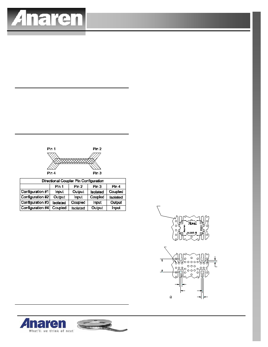
PIN CONFIGURATION
Most of the surface mount directional couplers have pin
orientations which are symmetrical. When a port is
chosen as the input port, automatically the output,
coupled and isolated ports are known. For example, if
the input port for a device was selected to be Pin 1, Pin 2
automatically becomes the output port, Pin 4 becomes
the coupled port, and Pin 3 is the isolated port. Similarly,
if Pin 3 was to be selected as the input port, the adjacent
port on the long side (Pin 4) is the output port, the
adjacent port on the short side (Pin 2) is the coupled port,
and the opposite port (Pin 1) is the isolated port. Any port
can be selected as the input port, as shown in the table
below, which shows every pin configuration possible.
MOUNTING
For optimal performance of the surface mount couplers,
there must be 50
transmission lines leading to and from
all of the RF ports. Also, there must be a very good
ground plane under the part to ensure proper electrical
performance. If either of these two conditions are not
satisfied, insertion loss, coupling, VSWR and directivity
may not meet published specifications.
Overall ground is improved if a dense population of plated
through holes connect the top and bottom ground layers
of the PCB. This minimizes ground inductance and
improves ground continuity as well as power handling.
Performance can also be improved when grounded
coplanar waveguide is used as the transmission medium
and a low loss dielectric is used. All of the Xinger
couplers are constructed from ceramic filled PTFE
composites which possess excellent electrical and
mechanical stability having X and Y thermal coefficient of
expansion (CTE) of 17 ppm/
o
C.
When a surface mount directional coupler is mounted to a
printed circuit board, the primary concerns are; insuring
the RF pads of the device are in contact with the circuit
trace of the PCB and insuring the ground plane of neither
the component nor the PCB is in contact with the RF
signal. As long as the geometry of the unit fits onto the
layout of the circuit trace on the PCB, and the conditions
of the previous paragraph are followed, the coupler's
performance is ensured. An example of how the PCB
footprint could look is shown below. In specific designs,
the 50
lines need to be adjusted to the unique dielectric
coefficients and varying thickness as well as adjustments
for pick and place equipment tolerances.
SUGGESTED FOOTPRINT
JA1305-5 Rev A Mounting Footprint
Dimensions are in Inches [Millimeters]
To insure proper electrical and thermal performance
there must be a ground plane under the part
.034 TYP
[0.86]
Multiple plated thru holes to ground plane
2x .313
[7.95]
.063 SQ TYP
[1.60]
2x .523
[13.28]
50 Transmission Line