
1.1W Mono Low-Voltage Audio Power Amplifier
Copyright
©
ANPEC Electronics Corp.
Rev. A.
5 -
Oct
.,
2005
APA0710/0711
www.anpec.com.tw
1
ANPEC reserves the right to make changes to improve reliability or manufacturability without notice, and advise
customers to obtain the latest version of relevant information to verify before placing orders.
The APA0710 is a bridged-tied load (BTL) or singled-
ended (SE) audio power amplifier developed especially
for low-voltage applications where internal speakers
and external earphone operation are required. The
APA0711 is a only BTL audio power amplifier developed
especially for low-voltage applications where internal
speakers are required. Operating with a 5V supply,
the APA0710/1 can deliver 1.1W of continuous power
into a BTL 8
load at 10% THD+N throughout voice
band frequencies. Although this device is characterized
out to 20kHz,its operation is optimized for narrow band
applications such as wireless communications. The
BTL configuration eliminates the need for external
coupling capacitors on the output in most applications,
which is particularly important for small battery-powered
equipment. A unique feature of the APA0710 is that it
allows the amplifier to switch from BTL to SE on the
fly when an earphone drive is required. This eliminates
complicated mechanical switching or auxiliary devices
just to drive the external load. This device features a
shutdown mode for power-sensitive applications with
special depop circuitry to eliminate speaker noise when
exiting shutdown mode. The APA0710/1 are available
in an 8-pin SOP and 8-pin MSOP-P with enhanced
thermal pad.
∑
Operating Voltage : 2.6V-5.5V
∑
APA0710 Compatible with TPA711
APA0711 Compatible with TPA751
∑
Bridge-Tied Load (BTL) or Single-Ended (SE)
Modes Operation (for APA0710 only)
∑
Supply Current
≠ I
DD
=1.3mA at V
DD
=5V ,BTL mode
≠ I
DD
=0.9mA at V
DD
=3.3V ,BTL mode
∑
Low Shutdown Current
≠ I
DD
=0.1
µ
A
∑
Low Distortion
≠ 630mW, at V
DD
=5V, BTL, R
L
=8
THD+N=0.15%
≠ 280mW, at V
DD
=3.3V, BTL, R
L
=8
THD+N=0.15%
∑
Output Power
at 1% THD+N
≠ 900mW, at V
DD
=5V, BTL, R
L
=8
≠ 400mW, at V
DD
=3.3V, BTL, R
L
=8
at 10% THD+N
≠1.1W at V
DD
=5V, BTL, R
L
=8
≠480mW at V
DD
=3.3V, BTL, R
L
=8
∑
Depop Circuitry Integrated
∑
Thermal Shutdown Protection and
Over Current Protection Circuitry
∑
High supply voltage ripple rejection
∑
Surface-Mount Packaging
≠ 8 pin MSOP-P (with enhanced thermal pad)
power package available
≠ SOP-8 package
∑
Lead Free Available (RoHS Compliant)
Features
General Description
Applications
∑
Mobil Phones
∑
PDAs
∑
Digital Camera
∑
Portable Electronic Devices
Copyright
©
ANPEC Electronics Corp.
Rev. A.
5 -
Oct
.,
2005
APA0710/0711
www.anpec.com.tw
2
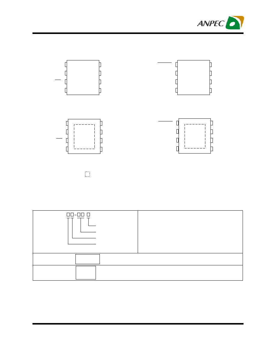
Ordering and Marking Information
APA0710/1
Handling Code
Temp. Range
Package Code
Package Code
K : SOP-8 XA : MSOP-8-P
Temp. Range
I : -40 to 85 C
Handling Code
TR : Tape & Reel
Lead Free Code
L : Lead Free Device Blank : Original Device
∞
APA0710/1 K :
APA0710/1
XXXXX
XXXXX - Date Code
XXXXX - Date Code
Lead Free Code
APA0710/1 XA :
A0710/1
XXX
XX
Pin Description
SOP-8
1
2
3
4
5
6
7
8
Shutdown
Bypass
SE/BTL
VO+
GND
V
DD
IN
VO-
APA0710
SOP-8
1
2
3
4
5
6
7
8
Shutdown
Bypass
IN+
VO+
GND
V
DD
IN-
VO-
APA0711
1
2
3
4
5
6
7
8
Shutdown
Bypass
IN+
VO+
GND
V
DD
IN-
VO-
1
2
3
4
5
6
7
8
Shutdown
Bypass
SE/BTL
VO+
GND
V
DD
IN
VO-
NC = No internal connection
= Thermal Pad
(connected to GND plane for better heat dissipation)
MSOP-8-P
APA0710
APA0711
MSOP-8-P
Note: ANPEC lead-free products contain molding compounds/die attach materials and 100% matte tin plate
termination finish; which are fully compliant with RoHS and compatible with both SnPb and lead-free soldiering
operations. ANPEC lead-free products meet or exceed the lead-free requirements of IPC/JEDEC J STD-020C
for MSL classification at lead-free peak reflow temperature.

Copyright
©
ANPEC Electronics Corp.
Rev. A.
5 -
Oct
.,
2005
APA0710/0711
www.anpec.com.tw
3
Block Diagram
+
_
+
_
C B
C I
R I
V
DD
C s
V
DD
/2
B y p a s s
S h u t d o w n
1
2
3
4
5
6
7
8
Vo+
Vo-
G N D
IN -
B i a s
C o n trol
R F
Audio
In p u t
V
DD
A P A 0 7 1 1
From S ys te m C o n t r o l
IN +
+
_
+
_
CB
CI
RI
V
DD
Cs
C
C
V
DD
/2
Bypass
Shutdown
SE/BTL
1
2
3
4
5
6
7
8
Vo+
Vo-
GND
IN
Bias
Control
RF
Audio
Input
V
DD
From System Control
From HP Jack
APA0710

Copyright
©
ANPEC Electronics Corp.
Rev. A.
5 -
Oct
.,
2005
APA0710/0711
www.anpec.com.tw
4
Symbol
Parameter
Test Conditions
Min.
Max.
Unit
V
DD
Supply Voltage
2.6
5.5
V
Shutdown, Shutdown
2.2
V
IH
High-Level Voltage
SE/BTL
0.9V
DD
V
Shutdown, Shutdown
0.4
V
IL
Low-Level Voltage
SE/BTL
0.9V
DD
-1
V
Recommended Operating Conditions
Thermal Characteristics
Symbol
Parameter
Value
Unit
R
THJA
Thermal Resistance from Junction to Ambient in Free Air
MSOP-8-P*
SOP-8
50
160
∞
C/W
Symbol
Parameter
Rating
Unit
V
DD
Supply Voltage
-0.3 to 6
V
V
IN
Input Voltage Range, Shutdown, SE/BTL
-0.3 to V
DD
+0.3
V
T
A
Operating Ambient Temperature Range
-40 to 85
∞
C
T
J
Maximum Junction Temperature
Internally Limited*
1
∞
C
T
STG
Storage Temperature Range
-65 to +150
∞
C
T
S
Soldering Temperature, 10 seconds
260
∞
C
V
ESD
Electrostatic Discharge
-2000 to 2000*
2
V
P
D
Power Dissipation
Internally Limited
W
Note:
1.APA0710/1 integrated internal thermal shutdown protection when junction temperature ramp up to 170∞C
2.Human body model: C=100pF, R=1500
, 3 positives pulses plus 3 negative pulses
3.Machine model: C=200pF, L=0.5
µ
F, 3 positive pulses plus 3 negative pulses
Absolute Maximum Ratings
(Over operating free-air temperature range unless otherwise noted.)
* 3.42in
2
printed circuit board with 20z trace and copper through 6 vias of 12mil diameter vias.
The thermal pad on the MSOP-8-P package with solder on the printed circuit board.
Copyright
©
ANPEC Electronics Corp.
Rev. A.
5 -
Oct
.,
2005
APA0710/0711
www.anpec.com.tw
5
APA0710/1
Symbol
Parameter
Test Conditions
Min.
Typ.
Max.
Unit
V
OO
Output Offset Voltage
R
L
= 8
, R
F
= 10k
20
mV
BTL mode, R
F
= 10k
0.9
1.8
I
DD
Supply Current
SE mode, R
F
= 10k
0.55
1.1
mA
I
DD(SD)
Supply Current,
Shutdown Mode
R
F
= 10k
0.1
2
µ
A
Shutdown, V
I
= V
DD
1
Shutdown, V
I
= V
DD
1
|IH|
SE/BTL, V
I
= V
DD
1
µ
A
Shutdown, V
I
= 0V
1
Shutdown, V
I
= 0V
1
|IL|
SE/BTL, V
I
= 0V
1
µ
A
Operating characteristic, V
DD
= 3.3V, T
A
= 25∞C, RL = 8
THD = 1%, BTL mode, R
L
= 8
400
P
O
Output Power
(Note 1)
THD = 1%, SE mode, R
L
= 32
40
mW
THD+N
Total Harmonic Distortion
Plus Noise
(Note 1)
P
O
= 280mW, BTL mode, R
L
= 8
0.15
%
Bom
Maximum Output Power
Bandwidth
Gain = 2, THD+N = 2%
20
kHz
B1
Unity-Gain Bandwidth
Open Loop
2
MHz
C
B
= 1
µ
F, BTL mode, R
L
= 8
74
PSRR
Power Supply Rejection
Ratio
(Note1)
C
B
= 1
µ
F, SE mode, R
L
= 8
61
dB
Vn
Noise Output Voltage
Gain = 1, C
B
= 0.1
µ
F
28
µ
V(rms)
T
WU
Wake-up time
C
B
= 1
µ
F
380
ms
Electrical Characteristics
Electrical Characteristics at Specified Free - Air Temperature
V
DD
= 3.3V, T
A
= 25∞C (unless otherwise noted)
V
DD
= 5V, T
A
= 25∞C (unless otherwise noted)
APA0710/1
Symbol
Parameter
Test Conditions
Min.
Typ.
Max.
Unit
V
OO
Output Offset Voltage
R
L
= 8
, R
F
= 10k
20
mV
BTL mode, R
F
= 10k
1.3
2.6
I
DD
Supply Current
SE mode, R
F
= 10k
0.75
1.5
mA
I
DD(SD)
Supply Current ,
Shutdown Mode
R
F
= 10k
0.1
2
µ
A