Copyright ANPEC Electronics Corp.
Rev. A.2 -Apr., 2004
APA2030/2031
www.anpec.com.tw
1
ANPEC reserves the right to make changes to improve reliability or manufacturability without notice, and advise
customers to obtain the latest version of relevant information to verify before placing orders.
Stereo 2.6W Audio Amplifier(With Gain Control)
Features
General Description
Applications
∑∑
∑∑
∑ Low operating current with 6mA
∑∑
∑∑
∑ Improved depop circuitry to eliminate turn-on
transients in outputs
∑∑
∑∑
∑ High PSRR
∑∑
∑∑
∑ Internal gain control, eliminate external components.
∑∑
∑∑
∑ 2.6W per channel output power into 3 load at 5V,
BTL mode
∑∑
∑∑
∑ Multiple input modes allowable selected by HP
/LINE pin (APA2030)
∑∑
∑∑
∑ Two output modes allowable with BTL and SE
modes selected by SE/BTL pin (for APA2030 only)
∑∑
∑∑
∑ Low current consumption in shutdown mode (50µ
A)
∑∑
∑∑
∑ Short Circuit Protection
∑∑
∑∑
∑ TSSOP-24-P (APA2030) and TSSOP-20-P
(APA2031) with thermal pad package.
∑∑
∑∑
∑ NoteBook PC
∑∑
∑∑
∑ LCD Monitor
APA2030/1 is a monolithic integrated circuit, which
provides internal gain control, and a stereo bridged
audio power amplifiers capable of producing 2.6W
(1.9W) into 3
with less than 10% (1.0%) THD+N.
By control the two gain setting pins, Gain0 and Gain1,
The amplifier can provide 6dB, 10dB, 15.6dB, and
21.6dB gain settings. The advantage of internal gain
setting can be less components and PCB area. Both
of the depop circuitry and the thermal shutdown pro-
tection circuitry are integrated in APA2030/1, that
reduces pops and clicks noise during power up or
shutdown mode operation. It also improved the power
off pop noise and protects the chip from being de-
stroyed by over temperature and short current failure.
To simplify the audio system design APA2030 com-
bines a stereo bridge-tied loads (BTL) mode for
speaker drive and a stereo single-end (SE) mode for
headphone drive into a single chip, where both modes
are easily switched by the SE/BTL input control pin
signal. Besides the multiple input selections is used
for portable audio system. APA2031 eliminates both
input selection and single-end (SE) mode function to
simplifying the design and save the PCB space.
APA2030/1
Handling Code
Tem p. Range
Package Code
Package Code
R : TSSO P-P *
Tem p. Range
I : - 40 to 85 C
Handling Code
TU : Tube TR : Tape & Reel
TY : Tray
Lead Free Code
L : Lead Free Device Blank : Original Device
∞
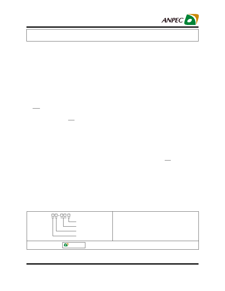
APA2030/1 R :
APA2030/1
XXXXX
XXXXX - Date Code
Lead Free Code
Ordering and Marking Information

Copyright ANPEC Electronics Corp.
Rev. A.2 - Apr., 2004
APA2030/2031
www.anpec.com.tw
2
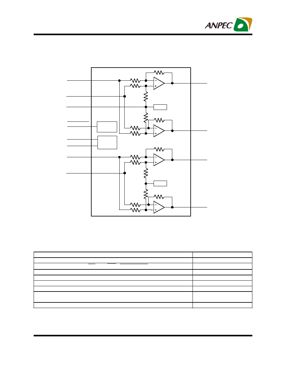
Block Diagram
Pin Assignment
APA2030
LOUT+ 4
LOUT- 9
21 ROUT+
16 ROUT-
RIN+ 8
LIN+ 10
BY PA SS 11
LLINEIN 5
23 RLINEIN
LHPIN 6
20 RHPIN
GA IN0 2
15 SE/BTL
22 SHUTDOWN
GA IN1 3
24 GND
13 GND
19 V
DD
18 PV
DD
PV
DD
7
GND 1
GND 12
14 PCBEEP
17 HP/LINE
T OP V ie w
(A PA 2030)
A P A 2030_P inOut
LOUT+ 4
LIN+ 9
17 RIN-
12 NC
LOUT- 8
BY PA SS 10
LIN- 5
19 SHUTDOWN
PV
D D
6
16 V
D D
GA IN0 2
11 GND
18 ROUT+
GA IN1 3
20 GND
15 PV
D D
14 ROUT-
RIN+ 7
GND 1
13 GND
T OP V ie w
(A PA 2031)
Sh u t d o w n
ckt
H P/L IN E
M U X
M U X
SE /B T L
LOUT+
LOUT-
ROUT+
ROUT-
LLINEIN
RLINEIN
LHPIN
RHPIN
HP/LINE
SE/BTL
SHUTDOW N
BY PA SS
PC - B EEP
ckt
PCBEEP
Vb ias
G ain
select ab le
Vb ias
LIN+
RIN+
GIA N1
GA IN0
A P A 2030_B lock
Copyright ANPEC Electronics Corp.
Rev. A.2 - Apr., 2004
APA2030/2031
www.anpec.com.tw
3
Parameter Rating
Supply voltage range, V
DD
, PV
DD
-0.3V to 6V
Input voltage range at SE/BTL, HP/LINE, SHUTDOWN,
-0.3V to V
DD
Operating ambient temperature range, T
A
-40∞C to 85∞C
Maximum junction temperature, T
J
Internal
Limited
Storage temperature range, T
STG
-65∞C to 150∞C
Soldering Temperature, 10 seconds, T
S
260∞C
Electrostatic Discharge, V
ESD
-3000 to 3000*1
-200 to 200*2
Power dissipation, P
D
Internal
Limited
Block Diagram
APA2031
Absolute Maximum Ratings
(Over operating free-air temperature range unless otherwise noted.)
Note:
*1. Human body model: C=100pF, R=1500
, 3 positives pulse plus 3 negative pulses
*2. Machine model: C=200pF, L=0.5mH, 3 positive pulses plus 3 negative pulses
Sh u td o wn
ckt
LOUT+
LOUT-
ROUT+
ROUT-
SHUTDOWN
BY PA SS
Vb ias
Gain
select ab le
Vb ias
LIN+
RIN+
LIN-
GA IN0
GA IN1
RIN-
APA2031_Block
Copyright ANPEC Electronics Corp.
Rev. A.2 - Apr., 2004
APA2030/2031
www.anpec.com.tw
4
Recommended Operating Conditions
Thermal Characteristics
Symbol Parameter Value
Unit
R
THJA
Thermal Resistance from Junction to Ambient in Free Air
TSSOP-P24*
TSSOP-P20*
45
48
∞C/W
Electrical Characteristics
(V
DD
=5V,-20∞C<T
A
<85∞C, unless otherwise noted.)
Symbol
Parameter
Test
Condition
Min. Typ. Max. Unit
V
DD
Supply
Voltage
3.3 5.5
V
SE/BTL = 0V
6
12
mA
I
DD
Supply
current
SE/BTL = 5V
4
8
mA
I
SD
Supply current in shutdown
mode
SHUTDOWN = 0V
50
300
µA
SHUTDOWN, GAIN0, GAIN1
2
V
V
IH
High level threshold Voltage
SE/BTL, HP/LINE
4 V
SHUTDOWN, GAIN0, GAIN1
0.8
V
V
IL
Low level threshold Voltage
SE/BTL, HP/LINE
3
V
I
I
Input
current
SHUTDOWN, SE/BTL,
HP/LINE, GAIN0, GAIN1
5
nA
V
ICM
Common mode Input voltage
VDD-1.0
V
V
OS
Output differential voltage
5
mV
PC_beep trigger level
1
Vp.p
* 5 in
2
printed circuit board with 2oz trace and copper pad through 9 25mil diameter vias.
The thermal pad on the TSSOP_P package with solder on the printed circuit board.
Supply Voltage, V
DD
...................................................................................................4.5V to 5.5V
Copyright ANPEC Electronics Corp.
Rev. A.2 - Apr., 2004
APA2030/2031
www.anpec.com.tw
5
Symbol
Parameter
Test Condition
Min.
Typ.
Max. Unit
THD=10%, Fin=1khz, RL=32
110
mW
P
O
Maximum output power
THD=1%, Fin=1khz, RL=32
90
mW
THD+N
Total harmonic distortion plus
noise
Po=75mW, RL=32
.Fin=1khz
0.03
%
PSRR
Power ripple rejection ratio
Vin=0.2Vrms, Rl=32
,
Cb=0.47
µf, f=120,
55
dB
SE/BTL attenuation
80
dB
xtalk
Channel separation
f=1khz, Cb=0.47
µf,
65
dB
HP/LINE input separation
f=1khz, Cb=0.47
µf, BTL
80
dB
S/N
Signal to noise ratio
Po=75mW, Rl=32
, A_weight,
100
dB
Symbol Parameter
Test
Condition Min. Typ. Max. Unit
THD=10%, F
in
=1khz, RL=3
2.6 W
THD=10%, F
in
=1khz, RL=4
2.3 W
THD=10%, F
in
=1khz, RL=
8
1.5 W
THD=1%, F
in
=1khz, RL=3
1.9 W
THD=1%, F
in
=1khz, RL=4
1.7 W
P
O
Maximum output power
THD=1%, F
in
=1khz, RL=8
1 1.1 W
Po=1.1W, RL=4
Fin=1khz
0.05 %
THD+N
Total harmonic distortion plus
noise
Po=0.7W, RL=8
, Fin=1khz
0.04 %
PSRR Power ripple rejection ratio
Vin=0.2Vrms, Rl=8
,
Cb=0.47
µf, f=120Hz
85 dB
xtalk Channel
separation
f=1khz, Cb=0.47
µf,
95 dB
HP/LINE input separation
f=1khz, Cb=0.47
µf,
80 dB
S/N
Signal to noise ratio
Po=1.1W, Rl=8
, A_weight
105 dB
Electical Characteristics (Cont.)
Operating Characteristics, BTL mode
Vdd=5V, T
A
=25∞C, Rl=4
, Gain=6dB, (Unless otherwise noted)
Operating Characteristics, SE mode ( for APA2030 only)
Vdd=5V, T
A
=25∞C, Rl=32
, Gain=4, 1dB, (Unless otherwise noted)