
Copyright
ANPEC Electronics Corp.
Rev. A.1 - Mar., 2003
APA2120/2121
www.anpec.com.tw
1
ANPEC reserves the right to make changes to improve reliability or manufacturability without notice, and advise
customers to obtain the latest version of relevant information to verify before placing orders.
Stereo 2-W Audio Power Amplifier (with DC_Volume Control)
Features
∑∑
∑∑
∑
Low operating current with 14mA
∑
Improved depop circuitry to eliminate turn-on
and turn off transients in outputs
∑
High PSRR
∑
32 steps volume adjustable by DC voltage with
hysteresis
∑
2W per channel output power into 4
load at 5V,
BTL mode
∑
Two output modes allowable with BTL and SE
modes selected by SE/BTL pin
∑
Low current consumption in shutdown mode
(50
µ
A)
∑
Short Circuit Protection
∑
Power off depop circuit integration
∑
TSSOP-24 with or without thermal pad package
Applications
General Description
Ordering and Marking Information
* TSSOP-P is a standard TSSOP package with a thermal pad exposure on the bottom of the package.
APA2120/1 is a monolithic integrated circuit, which
provides precise DC volume control, and a stereo
bridged audio power amplifiers capable of producing
2.7W(2.0W) into 3
with less than 10% (1.0%)
THD+N. The attenuator range of the volume control
in APA2120/1 is from 20dB (DC_Vol=0V) to -80dB
(DC_Vol=3.54V) with 32 steps. The advantage of
internal gain setting can be less components and PCB
area. Both of the depop circuitry and the thermal
shutdown protection circuitry are integrated in
APA2120/1, that reduce pops and clicks noise dur-
ing power up or shutdown mode operation. It also
improves the power off pop noise and protects the
chip from being destroyed by over temperature and
short current failure. To simplify the audio system
design, APA2120/1 combines a stereo bridge-tied
loads (BTL) mode for speaker drive and a stereo
single-end (SE) mode for headphone drive into a
single chip, where both modes are easily switched
by the SE/BTL input control pin signal. Besides, the
multiple input selection is used for portable audio
system.
∑
NoteBook PC
∑
LCD Monitor or TV
A P A 2 1 2 0 /1
H a n d lin g C o d e
T e m p . R a n g e
P a c k a g e C o d e
P a c k a g e C o d e
R : T S S O P -P *
T e m p . R a n g e
I : - 4 0 to 8 5 C
H a n d lin g C o d e
T U : T u b e T R : T a p e & R e e l
T Y : T ra y
∞
A P A 2 1 2 0 /1 R :
A P A 2 1 2 0 /1
X X X X X
X X X X X - D a te C o d e

Copyright
ANPEC Electronics Corp.
Rev. A.1 - Mar., 2003
APA2120/2121
www.anpec.com.tw
2
Block Diagram
(Over operating free-air temperature range unless otherwise noted.)
Symbol
Parameter
Rating
Unit
V
DD
Supply Voltage Range
-0.3 to 6
V
V
IN
Input Voltage Range, SE/BTL, HP/LINE,
SHUTDOWN, PCBEN
-0.3 to V
DD
+0.3
V
T
A
Operating Ambient Temperature Range
-40 to 85
∞
C
T
J
Maximum Junction Temperature
Intermal Limited*
1
∞
C
T
STG
Storage Temperature Range
-65 to +150
∞
C
T
S
Soldering Temperature,10 seconds
260
∞
C
V
ESD
Electrostatic Discharge
-3000 to 3000*
2
-200 to 200*
3
V
P
D
Power Dissipation
Intermal Limited
Absolute Maximum Ratings
S h u td o w n
ckt
H P /L IN E
V o lu m e
C o n tro l
M U X
M U X
S E /B T L
LOUT+
LOUT-
ROUT+
ROUT-
LLINEIN
RLINEIN
LHPIN
RHPIN
HP/LINE
SE/BTL
SHUTDOWN
RBYPASS
LBYPASS
VOLUME
B Y P A S S
BYPASS
P C -B E E P
ckt
PCBEEP
C lo ck G en
CLK
For APA2121
Note:
1.APA2120/1 integrated internal thermal shutdown protection when junction temperature ramp up to 150∞C
2.Human body model: C=100pF, R=1500
, 3 positives pulse plus 3 negative pulses
3.Machine model: C=200pF, L=0.5
µ
F, 3 positive pulses plus 3 negative pulses
Copyright
ANPEC Electronics Corp.
Rev. A.1 - Mar., 2003
APA2120/2121
www.anpec.com.tw
3
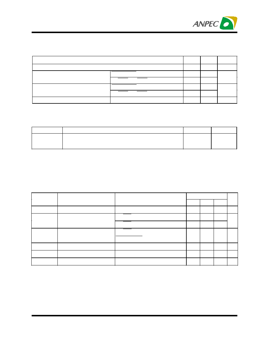
Recommended Operating Conditions
Min.
Max.
Unit
Supply Voltage, V
DD
4.5
5.5
V
SHUTDOWN, PCBEN
2
High level threshold voltage, V
IH
SE/BTL , HP/LINE
4
V
SHUTDOWN, PCBEN
1.0
Low level threshold voltage, V
IL
SE/BTL , HP/LINE
3
V
Common mode input voltage, V
ICM
V
DD
-1.0
V
V
DD
=5V, -20∞C<T
A
<85∞C
(unless otherwise noted)
Electrical Characteristics
Thermal Characteristics
Symbol
Parameter
Value
Unit
R
THJA
Thermal Resistance from Junction to Ambient in Free Air
TSSOP-P*
45
K/W
APA2120/1
Symbol
Parameter
Test Condition
Min. Typ. Max.
Unit
V
DD
Supply Voltage
4.5
5.5
V
SE/BTL=0V
14
25
I
DD
Supply Current
SE/BTL=5V
8.0
15
mA
I
SD
Supply Current in Shutdown
Mode
SE/BTL=5V
SHUTDOWN=0V
50
µ
A
I
IH
High input Current
900
nA
I
IL
Low Input Current
900
nA
V
OS
Output Differential Voltage
5
mV
* 5 in
2
printed circuit board with 2oz trace and copper pad through 9 25mil diameter vias.
The thermal pad on the TSSOP_P package with solder on the printed circuit board.

Copyright
ANPEC Electronics Corp.
Rev. A.1 - Mar., 2003
APA2120/2121
www.anpec.com.tw
4
APA2120/1
Symbol
Parameter
Test Condition
Min. Typ. Max.
Unit
THD=10%, R
L
=3
, Fin=1kHz
2.7
THD=10%, R
L
=4
, Fin=1kHz
2.3
THD=10%, R
L
=8
, Fin=1kHz
1.5
THD=1%, R
L
=3
, Fin=1kHz
2.0
THD=1%, R
L
=4
, Fin=1kHz
1.9
P
O
Maximum Output Power
THD=0.5%, R
L
=8
, Fin=1kHz
1
1.1
W
P
O
=1.5W, R
L
=4
, Fin=1kHz
0.05
THD+N Total Harmonic Distortion Plus
Noise
P
O
=1W, R
L
=8
, Fin=1kHz
0.07
%
PSRR Power Ripple Rejection Ratio
V
IN
=0.1Vrms, R
L
=8
, C
B
=1
µ
F,
Fin=120Hz
60
dB
Xtalk Channel Separation
C
B
=1
µ
F, R
L
=8
, Fin=1kHz
90
dB
S/N
Signal to Noise Ratio
P
O
=1.1W, R
L
=8
, A_wieght
95
dB
Operating Characteristics, BTL mode
V
DD
=5V,T
A
=25∞C,R
L
=4
, Gain=2V/V (unless otherwise noted)
Electrical Characteristics (Cont.)
Operating Characteristics, SE mode
V
DD
=5V,T
A
=25∞C,R
L
=4
, Gain=1V/V (unless otherwise noted)
APA2120/1
Symbol
Parameter
Test Condition
Min. Typ. Max.
Unit
THD=10%, R
L
=8
, Fin=1kHz
400
THD=10%, R
L
=32
, Fin=1kHz
110
THD=1%, R
L
=8
, Fin=1kHz
320
P
O
Maximum Output Power
THD=1%, R
L
=32
, Fin=1kHz
90
mW
P
O
=250mW, R
L
=8
, Fin=1kHz
0.08
THD+N Total Harmonic Distortion Plus
Noise
P
O
=75mW, R
L
=32
, Fin=1kHz
0.08
%
PSRR
Power Ripple Rejection Ratio
V
IN
=0.1Vrms, R
L
=8
, C
B
=1
µ
F,
Fin=120Hz
48
dB
Xtalk
Channel Separation
C
B
=1
µ
F, R
L
=32
, Fin=1kHz
100
dB
S/N
Signal to Noise Ratio
P
O
=75mW, SE, R
L
=32
, A_wieght
100
dB
