Class AB Stereo Headphone Driver
Copyright ANPEC Electronics Corp.
Rev. B.3 - Jun., 2003
APA2308
www.anpec.com.tw
1
ANPEC reserves the right to make changes to improve reliability or manufacturability without notice, and advise
customers to obtain the latest version of relevant information to verify before placing orders.
Features
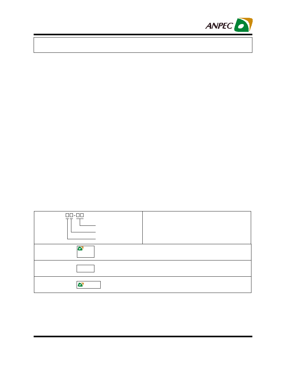
Ordering and Marking Information
The APA2308 is an integrated class AB stereo head-
phone driver contained in an SO-8, a DIP-8 or a
TSSOP-8 plastic package. The APA2308 is capable
of delivering 280mW of max. Output power to an 8
load or 110mW to a 32
load with less than 10%
(THD+N) from a 5V power supply. The device is fab-
ricated in a CMOS process and has been primarily
developed for portable digital audio applications .
Applications
∑
Portable Digital Audio
Gereral Description
∑∑
∑∑
∑
Operating Voltage
Single Supply 3V to 6V
Dual Supply
±1.5V to ± 3.0V
∑∑
∑∑
∑
High Signal-to-Noise Ratio 100dB
∑∑
∑∑
∑
Low Distortion -65dB
∑∑
∑∑
∑
Large Output Voltage Swing
∑∑
∑∑
∑
Excellent Power Supply Ripple Rejection
∑∑
∑∑
∑
Low Power Consumption
∑∑
∑∑
∑
Short-circuit Elimination
∑∑
∑∑
∑
Wide Temperature Range
∑∑
∑∑
∑
No Switch ON/OFF Clicks
∑∑
∑∑
∑
Available in 8 pin SOP ,DIP or TSSOP Package
A P A 2 3 08
P a ck a g e C o d e
J : P D IP - 8 K : S O P - 8
O : T S S O P - 8
T e m p . R an g e
I : - 4 0 to 8 5 C
H a nd lin g C o d e
T U : T u b e T R : T a p e & R e e l
∞
H a nd lin g C o d e
T e m p . R an g e
P a ck a g e C o d e
A P A 2 3 0 8 J :
A P A 2 3 0 8
X X X X X
X X X X X - D a te C o d e
A P A 2 3 0 8 K :
A P A 2 3 0 8
X X X X X
X X X X X - D a te C o d e
A P A 2 3 0 8 O :
A P A 2 3 0 8
X X X X X
X X X X X - D a te C o d e

Copyright ANPEC Electronics Corp.
Rev. B.3 - Jun., 2003
APA2308
www.anpec.com.tw
2
Thermal Characteristics
Absolute Maximum Ratings
Electrical Characteristics
V
DD
=5V , V
SS
=0V , T
A
=25∞C , f
i
=1kHz , R
L
=32
( unless otherwise noted)
Note : *1. Human body model : C=100pF , R=1500
, 3 positive pulses plus 3 negative pulses
Symbol
Parameter
Value
Unit
R
THJA
Thermal Resistance from Junction to Ambient in Free Air
DIP-8
SO-8
109
210
K/W
K/W
Symbol
Parameter
Rating
Unit
V
DD
Supply Voltage
7
V
T
SC(O)
Output Short-circuit Duration,at TA=25∞C,PTOT=1W
20
S
T
A
Operating Ambient Temperature range
-40 to 85
∞C
T
J
Maximum Junction Temperature
150
∞C
T
STG
Storage Temperature Range
-65 to +150
∞C
T
S
Soldering Temperature , 10 seconds
260
∞C
V
ESD
Electrostatic Discharge
-3000 to 3000
*1
V
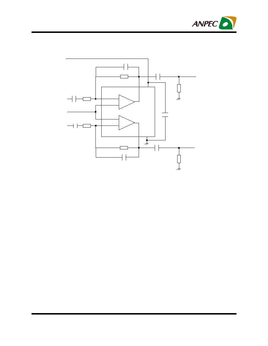
Block Diagram
APA2308
1
2
3
4
5
6
7
8
Out A
Inverting Input A
Non-inverting Input A
Non-inverting Input B
Out B
Inverting Input B
-
-
+
+
V
SS
V
DD
APA2308
Symbol
Parameter
Test Condition
Min.
Typ.
Max
Unit
Supply
Supply Voltage
Single
3.0
5.0
6.0
V
DD
Dual
±1.5
±2.5
±3.0
V
V
SS
Negative Supply Voltage
-1.5
-2.5
-3.0
V
I
DD
Supply Current
No Load
2.5
5
MA
P
TOT
Total Power Dissipation
No Load
12.5
25
mW

Copyright ANPEC Electronics Corp.
Rev. B.3 - Jun., 2003
APA2308
www.anpec.com.tw
3
APA2308
Symbol
Parameter
Test Condition
Min.
Typ.
Max
Unit
DC Characteristics
V
I(OS)
Input Offset Voltage
5
MV
I
BIAS
Input Bias Current
10
PA
V
CM
Common Mode Voltage
0
3.5
V
G
V
Open-loop Voltage Gain
R
L
=5k
75
dB
I
O
Max. Output Current
(THD+N)/S<0.1%
140
MA
R
O
Output Resistance
0.25
AC Characteristics
R
L
=32
*
1
0.25
4.75
V
O
Output Voltage Swing
R
L
=16
*
1
0.5
4.5
V
PSRR
Power Supply Rejection Ratio
F
i
=100Hz
V
RIPPLE(P-P)
=100mV
65
dB
\
CS
Channel Separation
R
L
=32
95
dB
C
L
Load Capacitance
200
pF
-65
-60
dB
(THD+N)/S Total Harmonic Distortion Plus
Noise to Signal Ratio
R
L
=32
*
2
0.05
0.1
S/N
Signal to Noise Ratio
90
100
dB
F
G
Unity Gain Frequency
R
L
=5k
5
MHz
P
O
Max. Output Power
(THD+N)/S<0.1%
84
mW
C
I
Input Capacitance
3
pF
B
Power Bandwidth
Unity Gain Inverting
20
kHz
Notes *1 : Values are proportional to V
DD
; (THD+N)/S < 0.1%
*2 : V
DD
=5.0V ; V
O(P-P)
=3.5V (at 0 dB)
Electrical Characteristics Cont.
V
DD
=5V, V
SS
=0V, T
A
=25∞C, f
i
=1kHz, R
L
=32
( unless otherwise noted)
Copyright ANPEC Electronics Corp.
Rev. B.3 - Jun., 2003
APA2308
www.anpec.com.tw
4
Test And Application Circuits
220pF
1
2
3
4
6
7
8
-
+
-
+
15k
15k
15k
15k
V
INA
V
INB
R
L
R
L
220
µF
100
µF
V
DD
V
OUTA
V
OUTB
220
µF
2.2
µF
220pF
5
2.2
µF
APA2308
V
REF
typ.1/2V
DD
Copyright ANPEC Electronics Corp.
Rev. B.3 - Jun., 2003
APA2308
www.anpec.com.tw
5
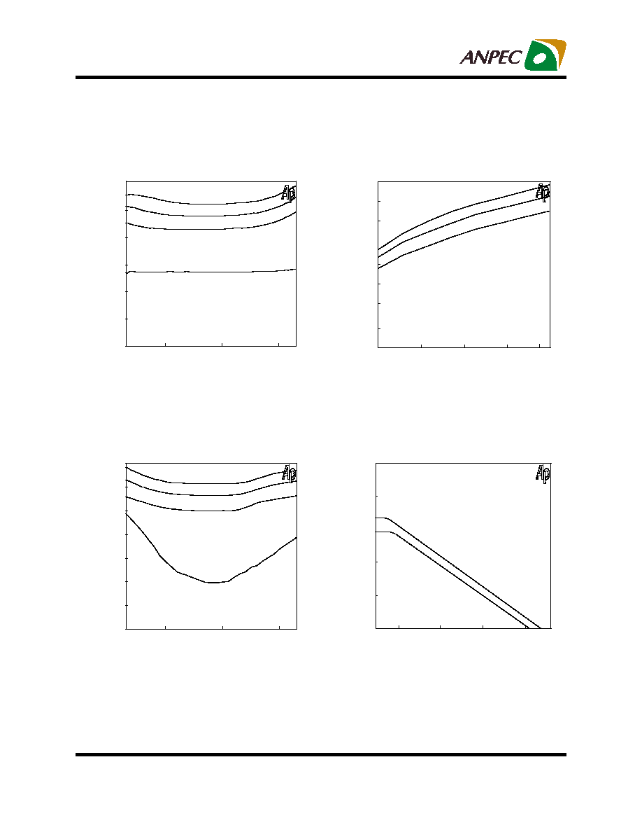
Typical Characteristics
Total Harmonic Distortion Plus Noise-to-
Signal Ratio as a Function of Input Fre-
quency
Output Power as a Function of Supply
Voltage
Crosstalk as a Function of Input
Frequency
Open Loop Gain as a Function of Input
Frequency
-120
-100
-80
100
1k
R
L
=5k
R
L
=32
R
L
=16
R
L
=8
10k
No load
+60
+20
+40
+80
1k
10k
100k
1M
R
L
=32
Frequency (Hz)
(THD+N) / S (dB)
V
DD
(Vrms)
P
O
(mW)
Frequency (Hz)
Xtalk
Frequency (Hz)
Gv (dB)
2
5
10
20
100
200
5.5
2.5
3.5
4.5
R
L
=8
R
L
=16
R
L
=32
-100
-80
-60
100
1k
10k
R
L
=8
R
L
=16
R
L
=32
R
L
=5k
p
o
=50mW
p
o
=50mW
p
o
=50mW
V
o(PP)
=3.5V