
Copyright
ANPEC Electronics Corp.
Rev. B.1 - Apr., 2003
APA3541/4
www.anpec.com.tw
1
ANPEC reserves the right to make changes to improve reliability or manufacturability without notice, and advise
customers to obtain the latest version of relevant information to verify before placing orders.
Class AB Stereo Headphone Driver with Mute
Ordering and Marking Information
Features
The APA3541/4 is an integrated class AB stereo
headphone driver contained in an SO-8 or a DIP-8
plastic package with Mute feature . Besides the com-
mon Mute feature , the APA3541/4 further integrates
a voltage divider inside the chip . Thus , the external
resistors can be eliminated . The APA3541 has a fixed
gain of 0dB and the APA3544 has a fixed gain of 6dB
so that external gain setting is unnecessary. The de-
vice is fabricated in a CMOS process and has been
primarily developed for portable digital audio appli-
cations .
∑∑
∑∑
∑
High Signal-to-Noise Ratio
∑∑
∑∑
∑
High Slew Rate
∑∑
∑∑
∑
Low Distortion
∑∑
∑∑
∑
Large Output Voltage Swing
∑∑
∑∑
∑
Flexible Mute Function
∑∑
∑∑
∑
Excellent Power Supply Ripple Rejection
∑∑
∑∑
∑
Low Power Consumption
∑∑
∑∑
∑
Short-circuit Elimination
∑∑
∑∑
∑
Wide Temperature Range
∑∑
∑∑
∑
No Switch ON/OFF Clicks
∑∑
∑∑
∑
Integrated Voltage Divider (V
DD
/2) to Eliminate
External Resistors
Applications
∑∑
∑∑
∑
Portable Digital Audio
General Description
A P A 3 5 41 /4
P a ck a g e C o d e
J : P D IP - 8 K : S O P - 8
Y : C h ip F ro m
T e m p . R an g e
I : - 4 0 to 8 5 C
H a nd lin g C o d e
T U : T u b e T R : T a p e & R e e l
∞
H a nd lin g C o d e
T e m p . R an g e
P a ck a g e C o d e
A P A 3 5 4 1/4 J :
A P A 3 5 4 1/4
X X X X X
X X X X X - D a te C o d e
A P A 3 5 4 1/4 K :
A P A 3 5 4 1/4
X X X X X
X X X X X - D a te C o d e

Copyright
ANPEC Electronics Corp.
Rev. B.1 -Apr., 2003
APA3541/4
www.anpec.com.tw
2
Symbol
Parameter
Rating
Unit
V
DD
Supply Voltage
7
V
t
SC(O)
Output Short-circuit Duration, at T
A
=25
∞
C, P
tot
=1W
20
S
T
A
Operating Ambient Temperature range
-40 to 85
∞
C
T
J
Maximum Junction Temperature
150
∞
C
T
STG
Storage Temperature Range
-65 to +150
∞
C
T
S
Soldering Temperature,10 seconds
300
∞
C
V
ESD
Electrostatic Discharge
-3000 to 3000
*1
V
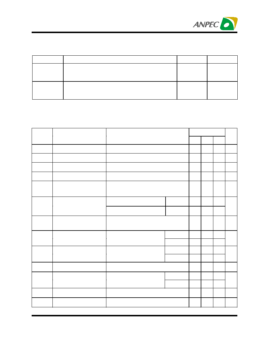
Pin Name
I/O
Function Description
Out A
O
A channel output pin
Mute
I
Chip disable control input, low active and high for normal operating
Input A
I
A channel input terminal
V
SS
Power ground pin
Input B
I
B channel input terminal
BIAS
I
Right channel bias input pin
OUT B
O
B channel output pin
V
DD
Power input pin
Absolute Maximum Ratings
Note: 1. Human body model : C=100pF, R=1500
, 3 positive pulses plus 3 negative pulses
Function Pin Description
Block Diagram
Input B
Out B
BIAS
M ute
Out A
Input A
BIAS
+
A
B
+
1
2
3
4
V
SS
5
6
7
8
V
D D
M U TE
0dB
(6dB)
0dB
(6dB)
180k
(
90k
)
180k
(
90k
)
* The values in parenthessis are for the APA3544.
Copyright
ANPEC Electronics Corp.
Rev. B.1 -Apr., 2003
APA3541/4
www.anpec.com.tw
3
Symbol
Parameter
Rating
Unit
R
THJA
Thermal Resistance from Junction to Ambient in Free Air
DIP-8
SOP-8
108
210
K/W
R
THJC
Thermal Resistance from Junction to Case
DIP-8
SOP-8
45
40
K/W
Electrical Characteristics
V
IN
=0dBV, V
CC
=5V, T
A
=25
∞
C, f=1kHz, R
L
=32
(unless otherwise noted)
APM3541/4
Symbol
Parameter
Test Condition
Min. Typ. Max.
Unit
V
DD
Supply Voltage
3.0
5.0
6.0
V
I
Q
Quiescent Current
VIN= 0 Vrms
3.5
5
mA
Imute
Mute Current
200
µ
A
V
TM
Mute Terminal Voltage
0.3
0.7
1.6
V
G
VCL
Differential Channel
Voltage Gain
-0.5
0
0.5
dB
Vin=1Vrms,f= 1kHz,RL=32
APA3541
-2
0
2
G
VCL
Voltage Gain
Vin=0.5Vrms, f=1kHz,Rl=32
APA3544
4
6
8
dB
THD
Total Harmonic Channel
Distortion Factor
BW<80kHz
0.03
0.1
%
APA3541
50
55
P
U1
Rated Output Power1
RL=32
,THD+N=0.1%,BW<8
0kHz
APA3544
75
80
mW
APA3541
105
110
P
U2
Rated Output Power2
RL=16
,THD+N=0.1%,BW<8
0kHz
APA3544
140
145
mW
V
NO
Output Noise Voltage
BW=20~20kHz , Vin=0Vrms
-93
-85
dBV
APA3541
-90
-95
CS
Channel Separation
F=1kHz
APA3544
-65
-70
dB
ATT
Mute Attenuation
VIN=1Vrms,f=1kHz,Mute=L
65
70
dB
RR
Ripple Rejection
F
RR
=100Hz,V
RR
=-20dBV
50
60
dB
Thermal Characteristics

Copyright
ANPEC Electronics Corp.
Rev. B.1 -Apr., 2003
APA3541/4
www.anpec.com.tw
4
Test and Application Circuit
+
BIAS
5
7
M UTE
6
8
V
DD
0dB(6dB)
B
A
APA3541
(APA3544)
220
µ
F
1
µ
F
1
µ
F
100
µ
F
220
µ
F
1 0 µ
F
1
µ
F
100k
V
INA
V
DD
O ut B
Input B
BIAS
V
INB
V
MUTE
H : Speaker Action
L : M ute on
O ut A
M ute
V
SS
+
Input A
4
3
2
1
0dB(6dB)

Copyright
ANPEC Electronics Corp.
Rev. B.1 -Apr., 2003
APA3541/4
www.anpec.com.tw
5
Typical Characteristics
Figure 1 : Supply Voltage : V
DD
(V)
Quiescent Current : I
Q
(mA)
Figure 2 : Supply Voltage : V
DD
(V)
Bias DC Voltage :V
bias
(V)
0
1
2
3
4
5
6
7
8
0
2
4
6
7
5
3
1
MUTE : OFF
MUTE : ON
R
L
=32
0
1
2
3
4
5
0
2
4
6
7
1
3
5
R
L
=32
Figure 3 : Mute Control Voltage : V
TM
(V)
Output Voltage : V
OUT
(dBV)
Figure 4 : Frequency :f (Hz)
Voltage Gain : G
VC
(dB)
10
100k
100
1k
10k
-12
+8
-10
-8
-6
-4
-2
+0
+2
+4
+6
APA3541
V
DD
=5V
V
IN
=0dBv
-80
-70
-60
-50
-40
-30
-20
-10
0
10
0
0.4
0.8
1.2
1.6
2
V
DD
=5V
V
IN
=0dBv
f =1 kHz
R
L
=32