Copyright
ANPEC Electronics Corp.
Rev. A.3 - Apr., 2001
APA4863
www.anpec.com.tw
1
ANPEC reserves the right to make changes to improve reliability or manufacturability without notice, and advise
customers to obtain the latest version of relevant information to verify before placing orders.
Stereo 2.2W Audio Power Amplifier
Features
∑∑
∑∑
∑
Depop Circuitry Integrated
∑∑
∑∑
∑
Thermal Shutdown Circuitry Integrated
∑∑
∑∑
∑
Bridge-Tied Load (BTL) or Single-Ended
(SE) Modes Operation
∑∑
∑∑
∑
Output Power at 1% THD+N, V
DD
=5V
- 2.2W/Ch (typ) into a 3
Load
- 1.8W/Ch (typ) into a 4
Load
- 1.2 W/Ch (typ) into a 8
Load
∑∑
∑∑
∑
Shutdown Control Mode, I
SD
= 0.5 µA
∑∑
∑∑
∑
Output Power (SE) at 0.5% THD+N, V
DD
=5V
- 90mW/Ch (typ.) into a 32
Load
∑∑
∑∑
∑
Various Power Packages Available
SOP, TSSOP, TSSOP-P
Applications
∑∑
∑∑
∑
Stereo Audio Power Amplifier for Notebook
Computer
∑∑
∑∑
∑
Portable Televisions
∑∑
∑∑
∑
Portable and Desktop Computers
General Description
Ordering Information
The APA4863 is a stereo bridge-tied audio power am-
plifier in various power packages , including SOP ,
TSSOP and TSSOP-P . When connecting to a 5V volt-
age supply , the APA4863 is capable of delivering
2.2W/1.8W/1.2W of continuous RMS power per chan-
nel into 3
/
4
/
8
bridge-tied loads with less than
1% THD+N respectively . When APA4863 operates
in the single-ended load , it is capable of delivering
90mW of continuous RMS power per channel into
32
load . The APA4863 simplifies design and frees
up board space for other features .
The APA4863 also served well in low-voltage appli-
cations , which provides 750mW (1% THD+N) per
channel into 4
loads with a 3.3V supply voltage .
Both of the depop circuitry and the thermal shutdown
protection circuitry are integrated in the APA4863 ,
that reduces pops and clicks noise during power up
and when using the shutdown mode and protects the
chip from being destroyed by over-temperature fail-
ure . To simplify the audio system design in note-
book computer applications , the APA4863 combines
a stereo bridge-tied loads mode for speaker drive and
a stereo single-end mode for headphone drive into a
single chip , where both modes are easily switched
by the HP-IN input control pin signal . For power sen-
sitive applications , the APA4863 also features a shut-
down function which keeps the supply current only
0.5 µA (typ.) .
Package Code
K: SOP
O: TSSOP R: TSSOP-P*
Temp. Range
I : -40 to 85 C
Handling Code
TU : Tube
TR : Tape & Reel TY: Tray
APA4863
Handling Code
Temp. Range
Package Code
∞
* TSSOP-P is a standard TSSOP package with a thermal pad exposed on the bottom of the package.
Copyright
ANPEC Electronics Corp.
Rev. A.3 - Apr., 2001
APA4863
www.anpec.com.tw
2
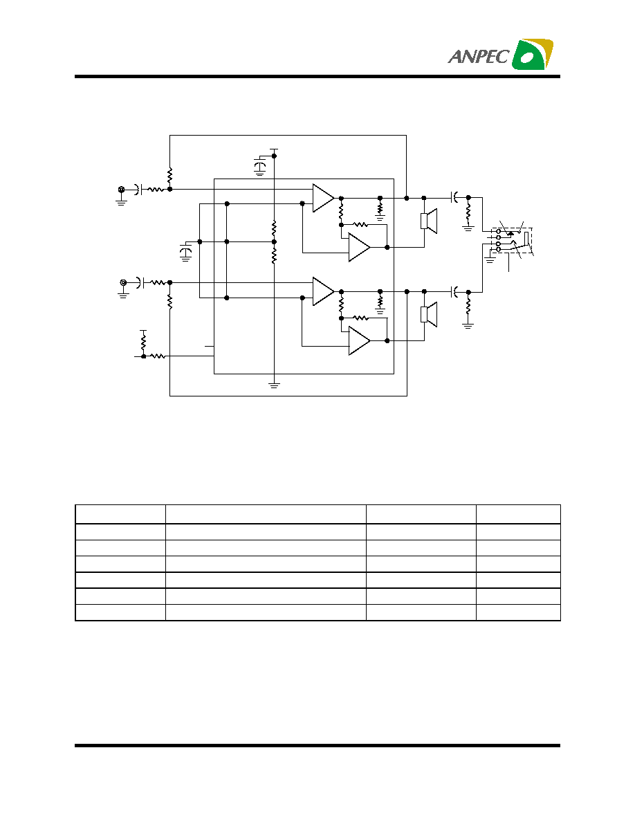
Block Diagram
(Over operating free-air temperature range unless otherwise noted.)
Absolute Maximum Ratings
Ring
10
4, 13
V
DD
5
0
50K
-
+
-
+
5
3
- IN A
+ OUT A
R
L
100
µ
F
To HP-IN Circuit
8
20K
20K
20K
-
+
-
+
12
14
+ OUT B
R
L
8
20K
20K
20K
- OUT B
- OUT A
C
O
+
1K
100
µ
F
C
O
+
1K
C
S
0.1
µ
F
V
DD
/ 2
6
C
B
2.2
µ
F
8
+ IN A*
Bypass
11
9
- IN B
+ IN B*
GND
2
,
7,15
20K
R
F
20K
R
F
C
1
R
1
Audio
Input
20K
1
µ
F
C
1
R
1
Audio
Input
20K
1
µ
F
16
1
100K
Shutdown
HP-IN
To Control Pin on
Headphone Jack
1
00
Headphone Jack
Sleeve
Control
Pin
Tip
V
DD
*
+INA and +INB pins are connected to Bypass pin inside the IC.
Note: *1. Human body model : C=100pF, R=1500
, 3 positive pulses plus 3 negative pulses
Symbol
Parameter
Rating
Unit
V
DD
Supply Voltage
6
V
T
A
Operating Ambient Temperature Range
-40 to 85
∞
C
T
J
Maximum Junction Temperature
150
∞
C
T
STG
Storage Temperature Range
-65 to +150
∞
C
T
S
Soldering Temperature,10 seconds
260
∞
C
V
ESD
Electrostatic Discharge
-2000 to 2000
*1
V
Copyright
ANPEC Electronics Corp.
Rev. A.3 - Apr., 2001
APA4863
www.anpec.com.tw
3
Min.
Typ.
Max.
Unit
Supply Voltage, V
DD
3
5
5.5
V
V
DD
=5V,
250mW/Ch average
power
4-
stereo BTL drive, with
proper PCB design
-20
85
Operating free-air
temperature, T
A
V
DD
=5V,
1.8 W/Ch average
power
4-
stereo BTL drive, with
proper PCB design and 300
CFM forced-air cooling
-20
85
∞
C
V
DD
=5 V
1.25
4.5
Common mode
input voltage, V
ICM
V
DD
=3.3V
1.25
2.7
V
Recommended Operating Conditions
Dissipation Rating Table
Package
Air Flow
(CFM)
Thermal Resistance
JA
(
∞
∞
∞
∞
C/W)
T
A
25
∞
∞
∞
∞
C
T
A
=70
∞
∞
∞
∞
C
SO16 +
0
50
2.5W
1.6W
TSSOP ++
0
200
73.2
66.6
1.7W
1.8W
1.1W
1.2W
TSSOP-P ++
0
200
37.6
32.3
3.3W
3.8W
2.1W
2.4W
+ : The parameter is measured with the recommended copper heat sink pattern on an 2-layer PCB, 11.7 in
2
3.0
◊
2.4 in
2
in PCB,
1oz.
copper, 3.0
◊
1.5 in
2
in coverage at Top-layer and Bottom-layer at 100% coverage (7.2in
2
).
++:The parameter is measured with the JEDEC standard test boards (multi-layer PCB).
APA4863
Symbol
Parameter
Test Conditions
Min.
Typ.
Max.
Unit
V
DD
Supply Voltage
3
5.5
V
I
DD
Quiescent Power Supply
Current
V
IN
=0V, I
O
=0A, HP-IN=0V
V
IN
=0V, I
O
=0A, HP-IN=4V
9
5
13.5
7.5
mA
I
SD
Shutdown Current
V
PIN1
= V
DD
5
0.5
µ
A
V
IH
Headphone High Input Voltage
4
V
V
IL
Headphone Low Input Voltage
0.8
V
Electical Characteristics
Electrical Characteristics for Entire IC
The following specifications apply for V
DD
= 5V unless otherwise noted. Limits apply for T
A
= 25∞C

Copyright
ANPEC Electronics Corp.
Rev. A.3 - Apr., 2001
APA4863
www.anpec.com.tw
4
Truth Table for Logic Inputs
Shutdown
HP-IN
APA4863 Mode
Low
Low
Bridge -Tied
Low
High
Single-Ended
High
Low
APA4863 Shutdown
High
High
APA4863 Shutdown
Electical Characteristics Cont.
APA4863
Symbol
Parameter
Test Conditions
Typ.
Unit
V
OS
Output Offset Voltage
V
IN
=0V
5
mV
THD=0.5%,
f=1kHz, R
L
=32
90
THD=1%,
f=1kHz, R
L
=8
320
P
O
Output Power
THD=10%,
f=1kHz, R
L
=8
400
mW
THD+N Total Harmonic Distortion
plus Noise
A
V
= -1 , P
O
=75mW, f=1kHz, R
L
=32
0.02
%
RSRR Power Supply Rejection
Ratio
V
RIPPLE
=200mV
RMS
, f=1kHz, C
B
=2.2
µ
F, R
L
=8
49
dB
X
TALK
Channel Separation
f=1kHz , C
B
=2.2
µ
F, P
O
=32mW, R
L
=32
85
dB
SNR
Signal-to-Noise Ratio
V
DD
=5V , P
O
=340mW, R
L
=8
95
dB
Electrical Characteristics for SE Mode Operation
The following specifications apply for V
DD
= 5V unless otherwise noted. Limits apply for T
A
= 25∞C
Electrical Characteristics for BTL Mode Operation
The following specifications apply for V
DD
= 5V unless otherwise noted. Limits apply for T
A
= 25∞C
APA4863 Unit
Symbol
Parameter
Test Conditions
Typ.
V
OS
Output Offset Voltage
V
IN
=0V
5
mV
THD=1%, f=1kHz
R
L
=3
R
L
=4
R
L
=8
2.2
1.8
1.2
P
O
Output Power
THD=10%, f=1kHz
R
L
=3
R
L
=4
R
L
=8
2.7
2.3
1.5
W
THD+N
Total Harmonic Distortion + Noise A
VD
=2, f=1kHz
R
L
=4
, P
O
=1.8W
R
L
=8
, P
O
=1W
0.3
0.15
%
RSRR
Power Supply Rejection Ratio
V
DD
=5V, V
RIPPLE
=200Mv
Rms
, R
L
=8
C
B
=2.2
µ
F
64
dB
X
TALK
Channel Separation
f=1kHz , C
B
=2.2
µ
F, P
O
=1W, R
L
=8
90
dB
SNR
Signal-to-Noise Ratio
V
DD
=5V, P
O
=1.1W, R
L
=8
95
dB
Copyright
ANPEC Electronics Corp.
Rev. A.3 - Apr., 2001
APA4863
www.anpec.com.tw
5
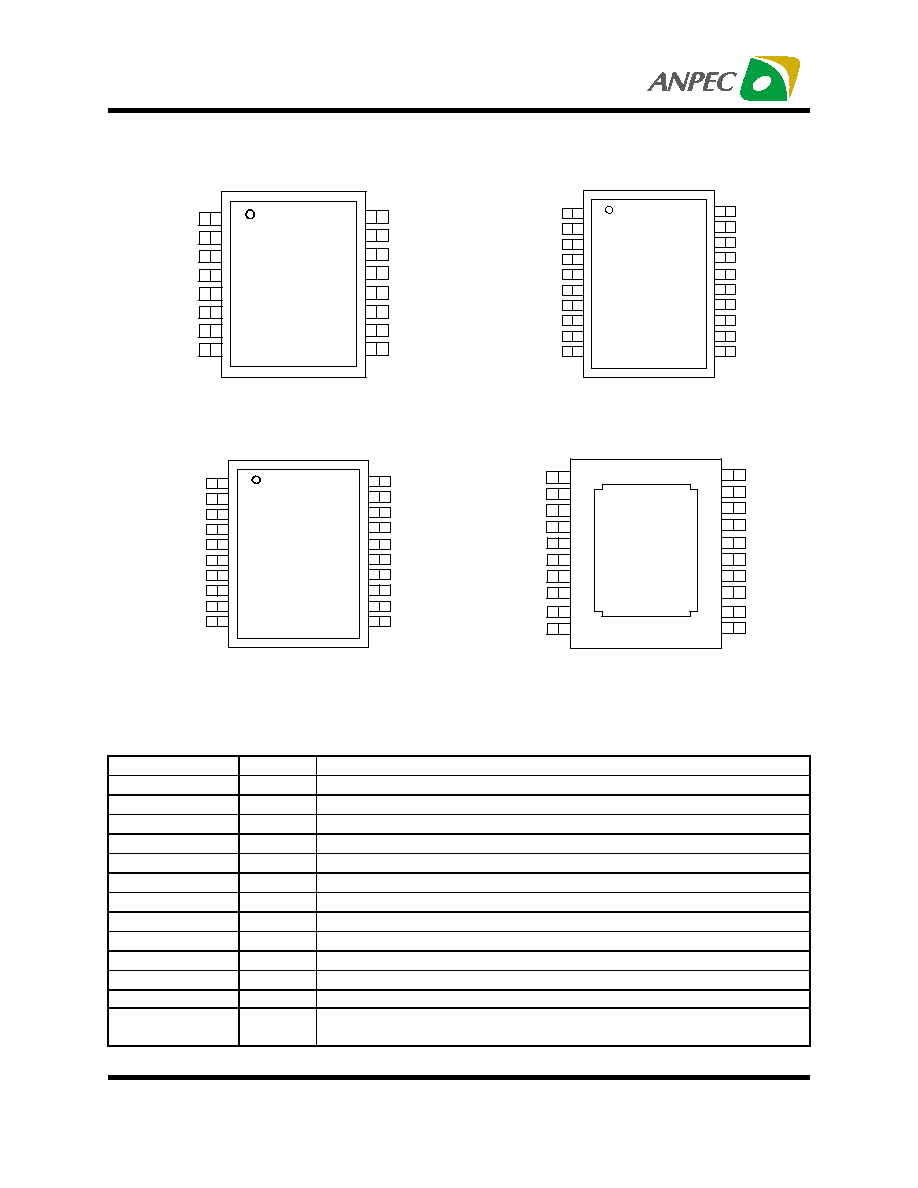
Pin Description
1
2
3
4
5
6
7
8
12
11
10
9
16
15
14
13
+ OUT A
SHUTDOWN
GND
V
DD
- IN A
- OUT A
GND
+ IN A
HP-IN
GND
V
DD
- IN B
- OUT B
BYPASS
+ IN B
+ OUT B
1
2
3
4
5
6
7
8
12
11
16
15
14
13
+ OUT A
SHUTDOWN
GND
V
DD
- IN A
- OUT A
GND
+ IN A
HP-IN
GND
V
DD
- IN B
- OUT B
BYPASS
+ IN B
+ OUT B
9
10
20
19
18
17
NC
NC
NC
NC
Top View
for SOP
Top View
for TSSOP
1
2
3
4
5
6
7
8
12
11
16
15
14
13
+ OUT A
SHUTDOWN
GND
V
DD
- IN A
- OUT A
GND
+ IN A
HP-IN
GND
V
DD
- IN B
- OUT B
BYPASS
+ IN B
+ OUT B
9
10
20
19
18
17
GND
GND
GND
GND
Thermal
Pad
Pin Description
Bottom View
Top View
for TSSOP -P
for TSSOP-P
Name
I/O
Description
GND
Ground connection of circuitry
V
DD
I
Supply voltage input
+ INA
I
Non-inverting input of channel A, connected to bypass pin inside the IC
- INA
I
Input pin of channel A
+ OUT A
O
A channel + output in BTL mode, high impedance in SE mode
- OUT A
O
A channel - output in BTL mode, + output in SE mode
+ IN B
I
Non-inverting input of channel B, connected to bypass pin inside the IC
- IN B
I
Input pin of channel B
+ OUT B
O
B channel + output in BTL mode, high impedance in SE mode
- OUT B
O
B channel - output in BTL mode, + output in SE mode
BYPASS
Connect to voltage divider for internal mid-supply bias
HP-IN
I
Headphone control pin input, hold high for single-ended mode operation
SHUTDOWN
I
Shutdown mode control pin input, places entire IC in shutdown mode
when held high, I
DD
= 0.5
µ
A