
Copyright
ANPEC Electronics Corp.
Rev. A.4 - Jan., 2003
APA4880
www.anpec.com.tw
1
ANPEC reserves the right to make changes to improve reliability or manufacturability without notice, and advise
customers to obtain the latest version of relevant information to verify before placing orders.
Stereo 330mW 8
Speak Driver With Mute
Ordering and Marking Information
The APA4880 is an integrated class AB stereo head-
phone amplifier contained in an SO-8 or a DIP-8 plas-
tic package. The APA4880 is capable of delivering
330mW of max. output power to an 8
load with less
than 10% (THD+N) from a 5V power supply. The
device has been primarily developed for portable digi-
tal audio applications. Both of the depop circuitry and
mute circuitry are integrated in the APA4880 , that
reduces pops and clicks noise during power up and
when using the mute mode(high active).
Applications
∑
Portable Digital Audio
∑
Personal Computers
∑
Microphone Preamplifier
∑
CD ROM Player
∑
Headphone Amplifier
Gereral Description
∑
Operating Voltage
Single Supply 3V to 7V
Dual Supply ±1.5V to ± 3.5V
∑
Depop Circuitry Integrated.
∑
High Signal-to-Noise Ratio 100dB
∑
High Slew Rate 5.5V/ms
∑
Low Distortion -66dB
∑
Output Power at 10% THD+N
into 8
330mW
into 16
200mW
∑
Large Output Voltage Swing
∑
Excellent Power Supply Ripple Rejection
∑
Low Power Consumption
∑
Short-circuit Elimination
∑
Wide Temperature Range
∑
No Switch ON/OFF Clicks
∑
Available in 8 pin SOP,TSSOP or PDIP
Package
Features
A P A 4 8 8 0
P a c k a g e C o d e
J : P D IP - 8 K : S O P - 8 O : T S S O P -8
T e m p . R a n g e
I : - 4 0 to 8 5 C
H a n d lin g C o d e
T U : T u b e T R : T a p e & R e e l
L e a d F re e C o d e
L : L e a d F re e D e v ic e B la n k : O rig in a l D e v ic e
∞
H a n d lin g C o d e
T e m p . R a n g e
P a c k a g e C o d e
A P A 4 8 8 0 J :
A P A 4 8 8 0
X X X X X
X X X X X - D a te C o d e
A P A 4 8 8 0 K /O :
A P A 4 8 8 0
X X X X X
X X X X X - D a te C o d e
L e a d F re e C o d e
Copyright
ANPEC Electronics Corp.
Rev. A.4 - Jan., 2003
APA4880
www.anpec.com.tw
2
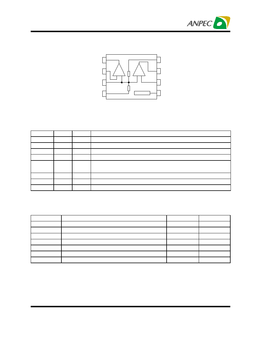
Mute
O u t B
INB
O u t A
Bypass
+
A
-
B
+ -
1
2
3
4
V
S S
5
6
8
V
D D
M U T E
7
INA
Block Diagram
APA4880
Absolute Maximum Ratings
Note : *1. Human body model : C=100pF , R=1500
, 3 positive pulses plus 3 negative pulses
Pin Function Description
Pin Name
No
I/O
Description
OUTA
1
O
Channel A output pin
INA
2
I
Audio input channel A
Bypass
3
I
Connect to voltage divider for internal mid_supply bias
VSS
4
Ground or negative supply voltage connection for circuitry.
Mute
5
I
mute mode control signal input, place entire IC in mute mode when held
high, Imute=140
µ
A
INB
6
I
Audio input channel B
OUTB
7
O
Channel B output pin
VDD
8
Supply voltage input pin
Symbol
Parameter
Rating
Unit
V
DD
Supply Voltage
5
V
T
SC(O)
Output Short-Circuit Duration , at T
A
=25
∞
C , P
TOT
=1W
20
S
T
A
Operating Ambient Temperature range
-40 to 85
∞
C
T
J
Maximum Junction Temperature
150
∞
C
T
STG
Storage Temperature Range
-65 to+150
∞
C
T
S
Soldering Temperature , 10 seconds
260
∞
C
V
ESD
Electrostatic Discharge
-3000 to 3000
*1
V

Copyright
ANPEC Electronics Corp.
Rev. A.4 - Jan., 2003
APA4880
www.anpec.com.tw
3
Thermal Characteristics
Symbol
Parameter
Value
Unit
R
THJA
Thermal Resistance from Junction to Ambient in Free Air
SO-8
TSSOP-8
PDIP-8
210
220
109
K/W
Electrical Characteristics
T
A
=25∞C, V
DD
=5V, V
SS
=0V, f=1kHz (unless otherwise noted)
APA4880
Symbol
Parameter
Test Conditions
Min.
Typ.
Max.
Unit
I
DD
Supply Current
No Load
3.0
mA
I
MUTE
Mute Current
V
PINS
140
uA
V
I(OS)
Input Offset Voltage
5
mV
AC Characteristics
(THD+N)/S Total Harmonic Distortion
plus Noise to Signal Ratio
P
O
=200mW , R
L
=8
, f=1kHz
P
O
=120mW , R
L
=16
, f=1kHz
P
O
=75mW , R
L
=32
, f=1kHz
0.05
0.04
0.03
%
Po
Output Power
(THD+N)/S=0.1% , f=1kHz
R
L
=8
R
L
=16
R
L
=32
(THD+N)/S=10% , f=1kHz
R
L
=8
R
L
=16
R
L
=32
240
150
85
330
200
110
mW
PSRR
Power Supply Rejection
Ratio
C
S
=2.2uF , V
RIPPLE
=200mV
RMS
,
f=120Hz
50
dB
ATT
Mute attenuation
Vin=1Vrms , R
L
=8
85
dB
Xtalk
Channel Separation
P
O
=200mV , R
L
=8
, Cb=2.2
µ
F
85
dB
Gv
Open Loop Gain
100
dB
Fg
Unity Gain Frequency
7
MHz
SR
Slew Rate
5.5
V/us
S/N
Signal to Noise Ratio
Vin=1Vrms , R
L
=8
20
uVrms

Copyright
ANPEC Electronics Corp.
Rev. A.3 - Jun., 2001
APA4880
www.anpec.com.tw
5
Typical Characteristics
0.01
1 0
0.02
0.05
0.1
0.2
0.5
1
2
5
1 0 m
5 0 0 m
2 0 m 3 0 m
5 0 m
8 0 m
2 0 0 m
0.01
1 0
0.02
0.05
0.1
0.2
0.5
1
2
5
1 0 m
3 0 0 m
2 0 m
3 0 m
5 0 m 7 0 m 1 0 0 m
0.01
1 0
0.02
0.05
0.1
0.2
0.5
1
2
5
1 0 m
2 0 0 m
2 0 m
3 0 m
5 0 m
7 0 m
1 0 0 m
0.01
0.02
0.05
0.1
0.2
0.5
1
2
5
1 0 m
3 0 0 m
2 0 m
3 0 m
5 0 m 7 0 m 1 0 0 m
THD+N-Total Harmonic Distortion+Noise (%)
V
DD
=5V
RL=32
Av=-1
THD+N-Total Harmonic Distortion+Noise (%)
THD+N-Total Harmonic Distortion+Noise (%)
THD+N-Total Harmonic Distortion+Noise (%)
Output Power (W)
f=20kHz
f=20Hz
f=1kHz
V
DD
=5V
RL=8
Av=-1
Output Power (W)
f=20kHz
f=20Hz
f=1kHz
V
DD
=5V
RL=16
Av=-1
Output Power (W)
f=20kHz
f=20Hz
f=1kHz
Output Power (W)
f=20kHz
f=20Hz
f=1kHz
V
DD
=3V
RL=8
Av=-1
