5A Low Dropout Fast Response Positive Adjustable Regulator and Fixed 3.3V
Copyright
ANPEC Electronics Corp.
Rev. B.9 - Aug., 2003
APL1084
www.anpec.com.tw
1
ANPEC reserves the right to make changes to improve reliability or manufacturability without notice, and advise
customers to obtain the latest version of relevant information to verify before placing orders.
!
Fast Transient Response
!
Guaranteed Dropout Voltage at Multiple Cur-
rents
!
Load Regulation :0.05% Typ.
!
Line Regulation : 0.03% Typ.
!
Low Dropout Voltage: 1.3V Typ. at I
OUT
=5A
!
Trimmed Current Limit : 5A Typ. at T
J
=125
∞
C
!
On-Chip Thermal Limiting : 150
∞
C Typ.
!
Standard 3-pin TO-220, TO-252 and TO-263
Power Packages
Features
General Description
Applications
!
Pentium
TM
Processor Supplies
!
powerPC
TM
Supplies
!
Low Voltage Logic Supplies
!
Battery-Powered Circuitry
!
Post Regulator for Switching Power Supply
applications, the APL1084 has been optimized. The
output available voltage range of adjustable version
is from 1.25~5.75V with an input supply below 7V,
and the fixed 3.3V output voltage device is also
available. Current limit is trimmed to ensure speci-
fied output current and controlled short-circuit current.
On-chip thermal limiting provides protection against
any combination of overload that would create ex-
cessive junction temperatures. The APL1084 is avail-
able in both the through-hole and surface mount ver-
sions of the industry standard 3-pin TO-220,TO-252
and TO-263 power packages.
Pin Description
Ordering Information
P a c k a g e C o d e
F : T O -2 2 0 G : T O -2 6 3 U : T O -2 5 2 Z : T O -2 64
T e m p . R a n g e
C : 0 to 7 0 C
H a n d lin g C o d e
T U : T u b e
T R : T a p e & R e e l
V o lta g e C o d e :
3 3 : 3 .3 V
B la n k : A d ju s ta b le V e rs io n
L e a d F re e C o d e
L : L e a d F re e D e vic e B la n k : O rg in a l D e vic e
∞
A P L1084 -
H a n d lin g C o d e
T e m p . R a n g e
P a c k a g e C o d e
V o lta g e C o d e
L e a d F re e C o d e
A P L 1 0 8 4 :
A P L 1 0 8 4
X X X X X
- D a te C o d e
X X X XX
A P L 1 0 8 4
X X X X X
3 3
A P L 1 0 8 4 - 3 3 :
- D a te C o d e
X X X X X
1
2
3
V
IN
V
OUT
ADJ
6)*EI8
OUT
1
2
3
V
IN
V
OUT
ADJ
6)*EI8
OUT
Front View APL1084
TO-263 Package
Front View APL1084
TO-264 Package
The APL1084 is a low dropout three-terminal adjust-
able regulator with 5A output current capability. In
order to obtain lower dropout voltage and faster tran-
sient response, which is critical for low voltage
1
2
3
V
IN
V
OUT
ADJ
6)*EI8
OUT
Front View APL1084
TO-220 Package
Front View APL1084
TO-252 Package
TAB is V
OUT
!
V
IN
V
OUT
ADJ

Copyright
ANPEC Electronics Corp.
Rev. B.9 - Aug., 2003
APL1084
www.anpec.com.tw
2
Symbol
Parameter
Rating
Unit
V
I
Input Voltage
7
V
T
J
Operating Junction Temperature Range
Control Section
Power Transistor
0 to 125
0 to 150
∞
C
T
STG
Storage Temperature Range
-65 to +150
∞
C
T
L
Lead Temperature (Soldering, 10 second)
260
∞
C
APL1084
Symbol
Parameter
Test Conditions
Min.
Typ.
Max.
Unit
V
REF
Reference Voltage
APL1084
1.5V
(V
IN
-V
OUT
)
5.75V,
10mA
I
OUT
5A, T
J
=0~125
∞
C
1.225(-2%) 1.250 1.275(+2%) V
V
OUT
Output Voltage
APL1084-3.3
10mA
I
OUT
5A, 4.75V
V
IN
7V,
T
J
=0~125
∞
C
3.235(-2%) 3.300 3.365(+2%) V
REG
LINE
Line Regulation
APL1084
APL1084-3.3
T
J
=0~125
∞
C, (Notes 1)
2.75V
V
IN
7V, I
OUT
=
10mA,
4.75V
V
IN
7V, I
OUT
=
0mA ,
0.03
0.2
%
REG
LOAD
Load Regulation
APL1084
APL1084-3.3
T
J
=25
∞
C, (Notes 1)
(V
IN
-V
OUT
)
=3V, 10mA
I
OUT
5A
V
I N
=5V, 0mA
I
OUT
5A
0.05
0.05
0.3
0.5
%
V
REF
=1% ,I
OUT
=3A ,T
J
=0~125
∞
C
1.2
1.4
V
V
D
Dropout Voltage
V
REF
=1% ,I
OUT
=5A ,T
J
=0~125
∞
C
1.3
1.5
(V
IN
-V
OUT
)
=1.7V, T
J
=
25
∞
C
T
J
=
125
∞
C
6.0
5.0
7.6
6.0
A
I
LIMIT
Current Limit
(V
IN
-V
OUT
)
=3V, T
J
=
25
∞
C
T
J
=
125
∞
C
6.5
5.5
8.2
6.5
I
ADJ
Adjust Pin Current
APL1084
(V
IN
-V
OUT
)
=3V, I
OUT
=10mA,
T
J
=0
125
∞
C
60
120
µ
A
I
ADJ
Adjust Pin Current
Change APL1084
1.5V
( V
IN
-V
OUT
)
5.75V,
10mA
I
OUT
5A
0.2
5
µ
A
I
LMIN
Minimum Load
Current APL1084
1.5V
( V
IN
-V
OUT
)
5.75V,
T
J
=0
125
∞
C
2
10
mA
I
Q
Quiescent Current
APL1084-3.3
V
I N
=5V
8
13
mA
PSRR Ripple Rejection
APL1084
APL1084-3.3
F=120Hz, C
out
=22
µ
F, Tant. ,
(V
IN
-V
OUT
)
=3V, I
OUT
=5A
F=120Hz, C
out
=22
µ
F, Tant. ,
(V
IN
=6.3V, I
OUT
=5A
60
dB
L
S
Long -Term
Stability
T
J
=
125
∞
C,1000Hrs.
0.03
1.0
%
Absolute Maximum Ratings
Electrical Characteristics

Copyright
ANPEC Electronics Corp.
Rev. B.9 - Aug., 2003
APL1084
www.anpec.com.tw
3
Application Circuits
* Required for stability
APL
1084
:C
=10
µ
F
* R1 is typically in range of 100
to 120
(2.75V~7V)
APL1084
V
IN
+
10µ
F
C
1
(1.250V/ 5A)
Solid Tantalum
C
2*
V
OUT
+
(5V)
APL1084
V
IN
+
10µ
F
C
1
(3.3V/ 5A)
V
OUT
Solid Tantalum
C
2*
+
R1
R2
V
OUT
=(R1+R2)/R1*1.250V
Typical Regulator
5V to 3.3V Regulator
Electrical Characteristics (Cont.)
NOTE 1: See thermal regulation specifications for changes in output voltage due to heating effects. Load and line regulations are
measured at a constant junction temperature by low duty cycle pulse testing.
NOTE 2 :The value could be varied when heat sink size is different. Use larger heat sink or larger PCB size , which improves
th
,TAB-A
, to improve overall thermal resistance (
th
,J-A
).
APL1084
Symbol
Parameter
Test Conditions
Min.
Typ.
Max.
Unit
V
N
RMS Output Noise(% of
V
OUT
)
T
J
=
25
∞
C,10Hz
F
10kHz
0.003
%
th,J-TAB
Thermal Resistance
Junction-to-Case, at TAB
(NOTE 2)
6.0
∞
C/ W
th,J-AMB
Thermal Resistance
Junction-to-Ambient
TO-263
TO-252
50
62.5
∞
C/ W
Copyright
ANPEC Electronics Corp.
Rev. B.9 - Aug., 2003
APL1084
www.anpec.com.tw
5
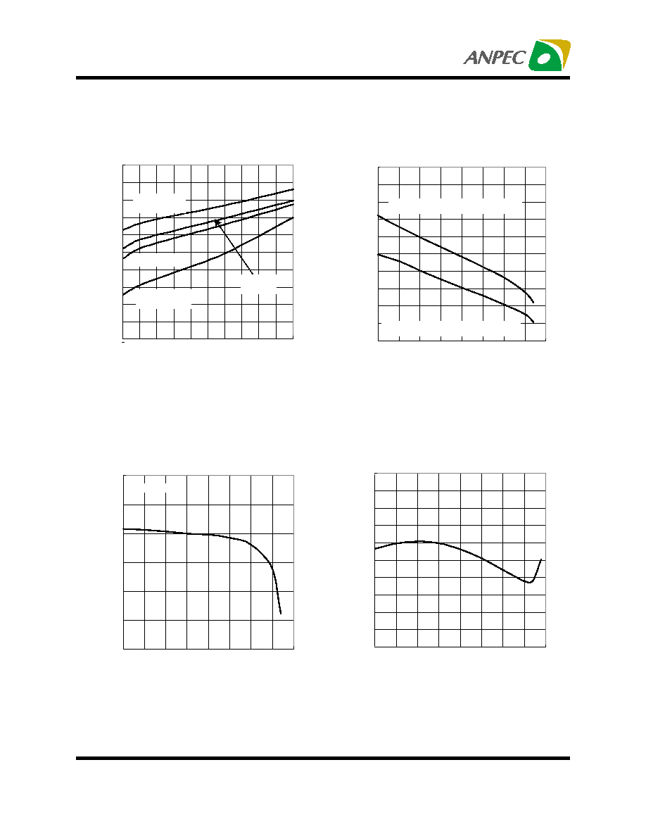
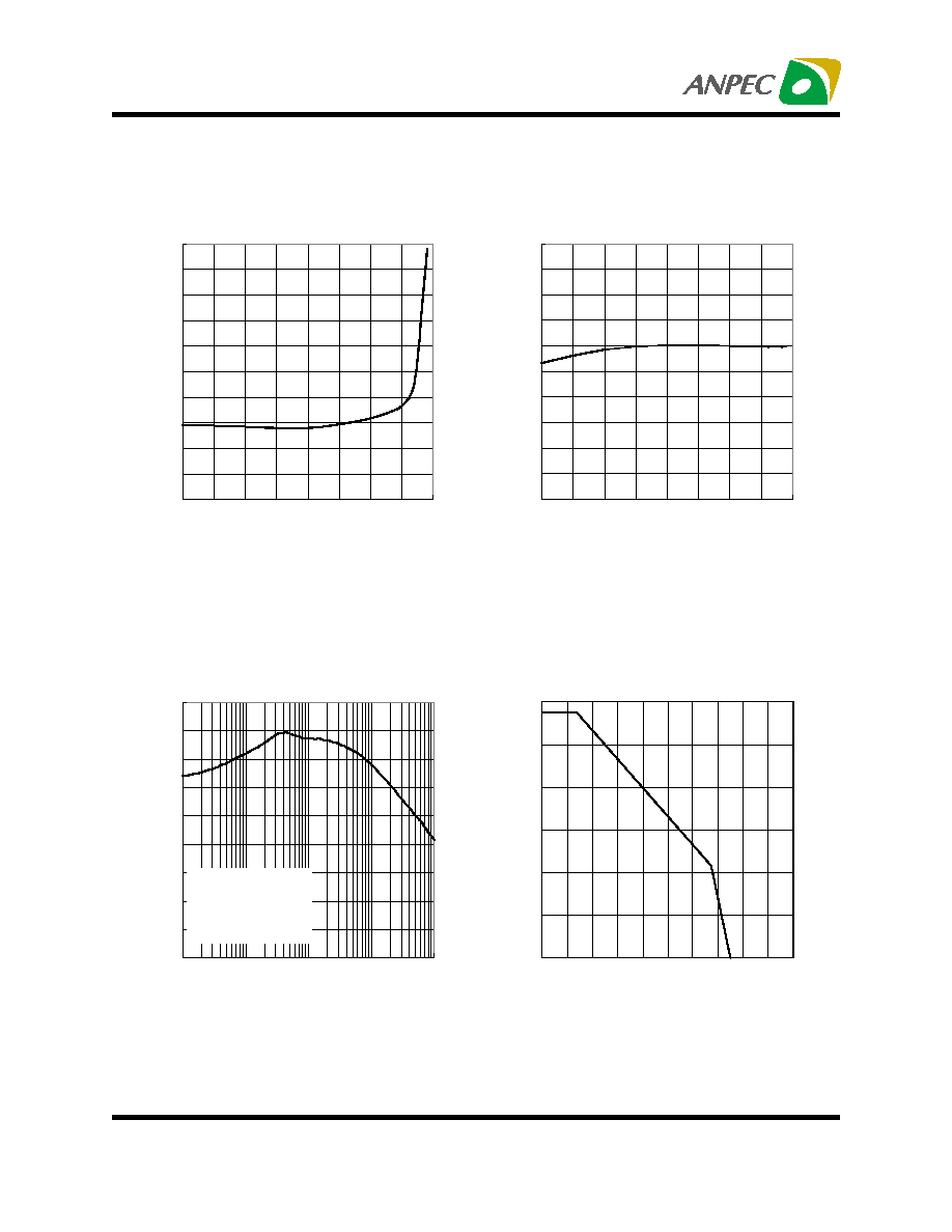
Typical Characteristics (Cont.)
-50
0
50
100
150
0
1
2
3
4
5
Temperature (
∞
C)
-50
0
50
100
150
0
10
20
30
40
50
60
70
80
90
100
Temperature (
∞
C)
V
IN
-V
OUT
= 3V
V
RIPPLE(p-p)
= 1V
I
OUT
= 5A
10
100
1k
10k
100k
0
10
20
30
40
50
60
70
80
90
Minimum Load Current vs Temperature
Minimum
Load
Current
(
mA)
Adjust Pin Current vs Temperature
Adjust
Pin
Current
(
µ
A)
Ripple Rejection vs Frequency
Ripple
Rejection
(dB)
Frequency (Hz)
#
%
'
!
#
#
#
#
!
Maximum Power Dissipation*
Power
(W)
Case Temperature (
∞
C)
* as Limited by Maximum Jcnction Temperature