
Copyright
ANPEC Electronics Corp.
Rev. A.3 - Jun., 2003
APL1117D/R
www.anpec.com.tw
1
ANPEC reserves the right to make changes to improve reliability or manufacturability without notice, and advise
customers to obtain the latest version of relevant information to verify before placing orders.
1A, Low Dropout Fast Response Positive Regulator Fixed 3.3V and 5.0V
∑∑
∑∑
∑
Guaranteed Output Voltage Accuracy within 2%
∑∑
∑∑
∑
Fast Transient Response
∑∑
∑∑
∑
Guaranteed Dropout Voltage at Multiple Cur-
rents
∑∑
∑∑
∑
Load Regulation : 0.1% Typ.
∑∑
∑∑
∑
Line Regulation : 0.03% Typ.
∑∑
∑∑
∑
Low Dropout Voltage : 1.2V Typ. at I
OUT
=0.8A
∑∑
∑∑
∑
Current Limit : 1A Typ. at T
J
=125
∞
C
∑∑
∑∑
∑
On-Chip Thermal Limiting : 150
∞
C Typ.
∑∑
∑∑
∑
Standard 3-pin SOT-223 and TO-252 Power
Packages
Features
Applications
∑∑
∑∑
∑
Active SCSI Terminators
∑∑
∑∑
∑
Low Voltage Logic Supplies
∑∑
∑∑
∑
Battery-Powered Circuitry
∑∑
∑∑
∑
Post Regulator for Switching Power Supply
General Description
The APL1117D/R is a low dropout three-terminal fixed
3.3V and 5.0V regulators with 1A output current
capability. In order to obtain lower dropout voltage
and faster transient response, which is critical for
low voltage applications , the APL1117D/R has been
optimized. The dropout voltage is guaranteed at a
maximum of 1.3V at 0.8A. Current limit is trimmed to
ensure specified output current and controlled short-
circuit current. On-chip thermal limiting provides pro-
tection against any combination of overload that would
create excessive junction temperatures. The
APL1117D/R is available in the industry standard 3-
pin SOT-223 and TO-252 the low profile surface mount
packages which can be used in applications where
space is limited.
Pin Description
Front View for TO-252
1
2
3
1
2
3
Front View for SOT-223
APL1117D GND V
OUT
V
IN
APL1117R V
IN
GND V
OUT
APL1117D GND V
OUT
V
IN
APL1117R V
IN
GND V
OUT

Copyright
ANPEC Electronics Corp.
Rev. A.3 - Jun., 2003
APL1117D/R
www.anpec.com.tw
2
P a c k a g e C o d e
U : T O -2 5 2 V : S O T -2 2 3
T e m p . R a n g e
C : 0 to 7 0 C
H a n d lin g C o d e
T U : T u b e T R : T a p e & R e e l
V o lta g e C o d e
3 3 : 3 .3 V 5 0 : 5 .0 V
L e a d F re e C o d e
L : L e a d F re e D e v ic e B la n k : O rig in a l D e v ic e
∞
A P L 1 1 1 7 D /R -
H a n d lin g C o d e
T e m p . R a n g e
P a c k a g e C o d e
V o lta g e C o d e
X X X X X - D a te C o d e
A P L 1 1 1 7 D /R -3 3 U :
A P L 1 1 1 7 D /R
X X X X X
- D a te C o d e
X X X X X
A P L 1 1 1 7 D /R
X X X X X 3 3
X X X X X - D a te C o d e
3 3
A P L 1 1 1 7 D /R -5 0 U :
A P L 1 1 1 7 D /R
X X X X X
- D a te C o d e
X X X X X
5 0
A P L 1 1 1 7 D /R -3 3 U :
A P L 1 1 1 7 D /R -5 0 U :
A P L 1 1 1 7 D /R
X X X X X 5 0
L e a d F re e C o d e
Ordering and Marking Information
Symbol
Parameter
Rating
Unit
V
I
Input Voltage
13.2
V
T
J
Operating Junction Temperature Range
Control Section
Power Transistor
0 to 125
0 to 150
∞
C
T
STG
Storage Temperature Range
-65 to +150
∞
C
T
L
Lead Temperature (Soldering, 10 second)
260
∞
C
Absolute Maximum Ratings
Electrical Characteristics
APL1117D/R
Sym bol
Param eter
Test C onditions
M in.
Typ. M ax.
Unit
APL1117D/R-33
3.235 3.300 3.365
V
OU T
APL1117D/R-50
T
J
=0~125
∞
C,
0
I
OU T
0.8A, 4.75V
V
IN
12V
4.900 5.000 5.100
V
REG
LINE
Line Regulation
T
J
=0~125
∞
C,
I
OU T
=0.8A, 4.75V
V
IN
7.75V
(Note1)
1
6
m V
REG
LO AD
Load Regulation
T
J
=0~125
∞
C,
V
IN
=4.75A, 0V
I
OU T
0.8A
(N ote1)
1
10
m V
V
D
Dropout Voltage
I
OU T
0.8A,T
J
=0~125∞C
1.2
1.3
V
I
LIMT
Current Lim it
(V
IN
-V
OU T
)=5V, T
J
=25∞C
1
A
PSR R
Ripple Rejection
F
RIPPLE
=120H z, V
RIPPLE
=1
VP-P
(V
IN
-V
OU T
)=3V,T
J
=0~125∞C
60
75
dB
T
R
Therm al Regulation T
J
=25∞C, 30m s Pulse
0.01
% /W
T
S
Tem perature
Stability
0.5
%
L
S
Long -Term
Stability
T
J
=125∞C, 1000Hrs
0.3
%
Copyright
ANPEC Electronics Corp.
Rev. A.3 - Jun., 2003
APL1117D/R
www.anpec.com.tw
3
APL1117D/R
Symbol
Parameter
Test Conditions
Min.
Typ. Max.
Unit
V
N
RMS Output Noise
T
J
=25
∞
C,10Hz
F
10kHz, (% of V
OUT
)
0.003
%
th
Thermal Resistance Junction to Case, at Tab
Junction to ambient
15
50
∞
C/ W
OT
Over Temperature
Point
150
∞
C
Quiescent Current
T
J
=0~125
∞
C,
V
IN
12V
5.5
10
mA
Note 1: See thermal regulation specifications for changes in output voltage due to heating effects. Load line regulations are mea-
sured at a constant junction temperature by low duty cycle pulse testing.
Note 2: Dropout voltage is specified over the full output current range of the device. Dropout voltage is defined as the minimum input/
output differential measured at the specified output current. Test points and limits are also shown on the Dropout Voltage curve.
Note 3: Minimum load current is defined as the minimum output current required to maintain regulation.
Electrical Characteristics
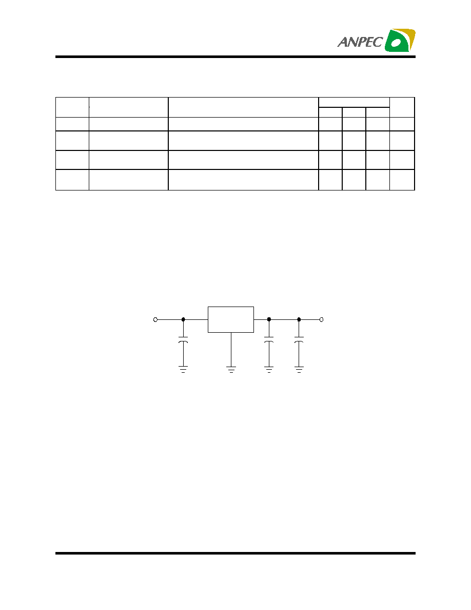
Application Schematic
APL1117D/R
C
OUT1
0.1uF
V
IN
=5~12V
V
OUT
C
IN
10uF
C
OUT2
10uF
+
+
+
Copyright
ANPEC Electronics Corp.
Rev. A.3 - Jun., 2003
APL1117D/R
www.anpec.com.tw
4
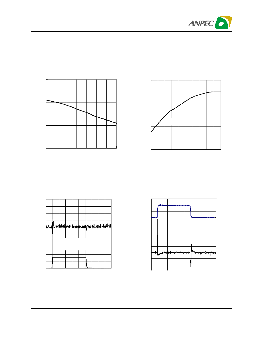
Typical Characteristics
2
3
4
5
6
7
8
-5 0
0
5 0
1 0 0
1 2 5
-2 5
2 5
7 5
Temperature (∞C)
Input Current (mA)
Input Current vs. Temperature
0.7
0.8
0.9
1
1.1
1.2
1.3
-50
-30
-10
10
30
50
70
90
110
130
150
Current Limit vs. Temperature
Temperature (∞C)
Current Limit (mA)
Vin-Vout=5V
0
0.5
1
1.5
2
2.5
3
3.5
4
4.5
5
-100
0
100
200
300
400
500
600
700
800
900
-0.03
-0.02
-0.01
0
0.01
0.02
-20
30
80
130
180
-0.05
0
0.05
0.1
0.15
0
1
2
3
4
5
6
Load Transient Response
Output Current (A)
Output V
oltage Deviation (V)
Time (
µ
s)
Line Transient Response
Input V
oltage (V)
Output V
oltage Deviation (V)
Time (
µ
s)
C
IN
=10uF
Cout=10uF Tantalum
V
IN
=5V
C
IN
=10uF
Cout=10uF Tantalum
I
OUT
=0.1A
V
out
=3.3V
V
out
=3.3V
V
out
=3.3V
V
out
=3.3V

Copyright
ANPEC Electronics Corp.
Rev. A.3 - Jun., 2003
APL1117D/R
www.anpec.com.tw
5
1
1.02
1.04
1.06
1.08
1.1
1.12
4
5
6
7
8
9
10
11
12
13
Typical Characteristics
Output Voltage vs. Input Voltage
Outputt V
oltage (V)
Dropout Voltage vs. Output Current
Output Current (A)
Dropout V
oltage (V)
Iutput Voltage (V)
0
0.5
1
1.5
2
2.5
3
3.5
0
1
2
3
4
5
6
7
8
9
0
1
2
3
4
5
6
0
2
4
6
8
1 0
Current Limit vs. Input Voltage
Input Voltage (V)
Input Current vs. Input Voltage
Input Voltage (V)
Input Current (mA)
Current Limit (A)
0.9
0.95
1
1.05
1.1
1.15
1.2
1.25
1.3
0
0.2
0.4
0.6
0.8
1
V
out
=3.3V
V
out
=3.3V
V
out
=3.3V
V
out
=3.3V