DUAL INPUT LOW DROPOUT REGULATOR
Copyright
ANPEC Electronics Corp.
Rev. A.4 - Apr., 2003
APL1582
www.anpec.com.tw
1
ANPEC reserves the right to make changes to improve reliability or manufacturability without notice, and advise
customers to obtain the latest version of relevant information to verify before placing orders.
Features
General Description
The APL1582 of high performance positive voltage
regulators are designed for use in applications
requiring very low dropout voltage at 3Amps .
The APL1582 can provide a output voltage at the range
of 1.25V to 2.55V , where both 5V and 3.3V voltage
supplies are available .
The superior dropout characteristics result in reduced
heat dissipation compared to regular LDOs. The
APL1582 also provides excellent regulation over line ,
load , and temperature variations.
Current limit is trimmed to ensure specified output
current and controlled short-circuit current . On-chip
thermal limiting provides protection against any
combination of overload that would create excessive
junction temperature .
The APL1582 is available in both the through-hole
and surface mount versions of the industry standard
5-Pin TO-220, TO-252 and TO-263 power packages .
Applications
∑
Microprocessor Supplies
∑
!
Chip Set Supplies
∑
VGA Card Power
∑
LCD Monitor Power
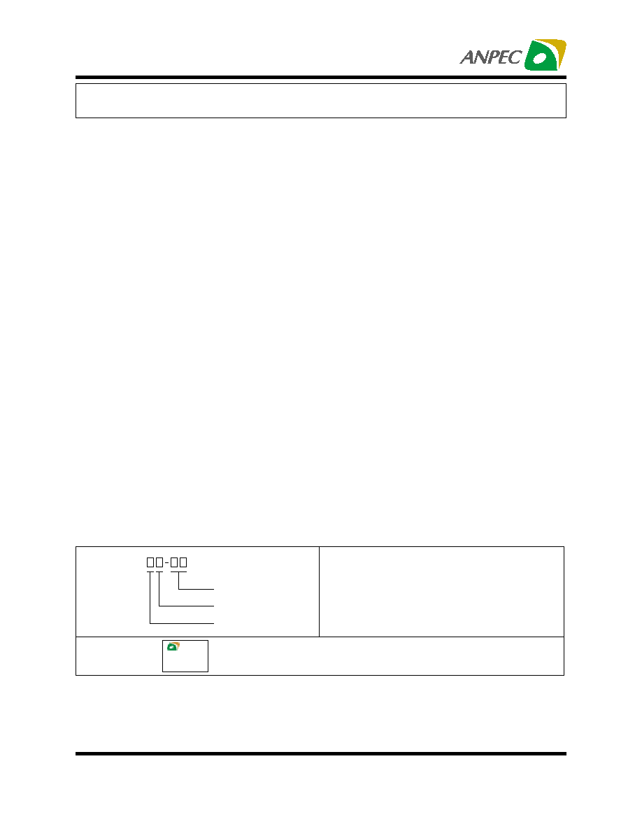
Ordering and Marking Information
APL1582
Package Code
F : TO-220-5 G : TO-263-5
U : TO-252-5
Temp. Range
C : 0 to 70 C
Handling Code
TU : Tube TR : Tape & Reel
Handling Code
Temp. Range
Package Code
APL1582
XXXXX
APL1582 F/G/U :
XXXXX - Date Code
∑∑
∑∑
∑
450mV typ. Dropout at 3A in dual power
voltage mode
∑∑
∑∑
∑
Remote Sense Pin Available
∑∑
∑∑
∑
2% Accuracy Over Temperature Range
∑∑
∑∑
∑
Build-in Over Temperature Protection
∑∑
∑∑
∑
Build-in Current Limit
∑∑
∑∑
∑
5 Pin TO-220, TO-252 and TO-263 Packages
∑∑
∑∑
∑
No Supply Sequencing Problems in Dual
Supply Mode
∞
Copyright
ANPEC Electronics Corp.
Rev. A.4 - Apr., 2003
APL1582
www.anpec.com.tw
2
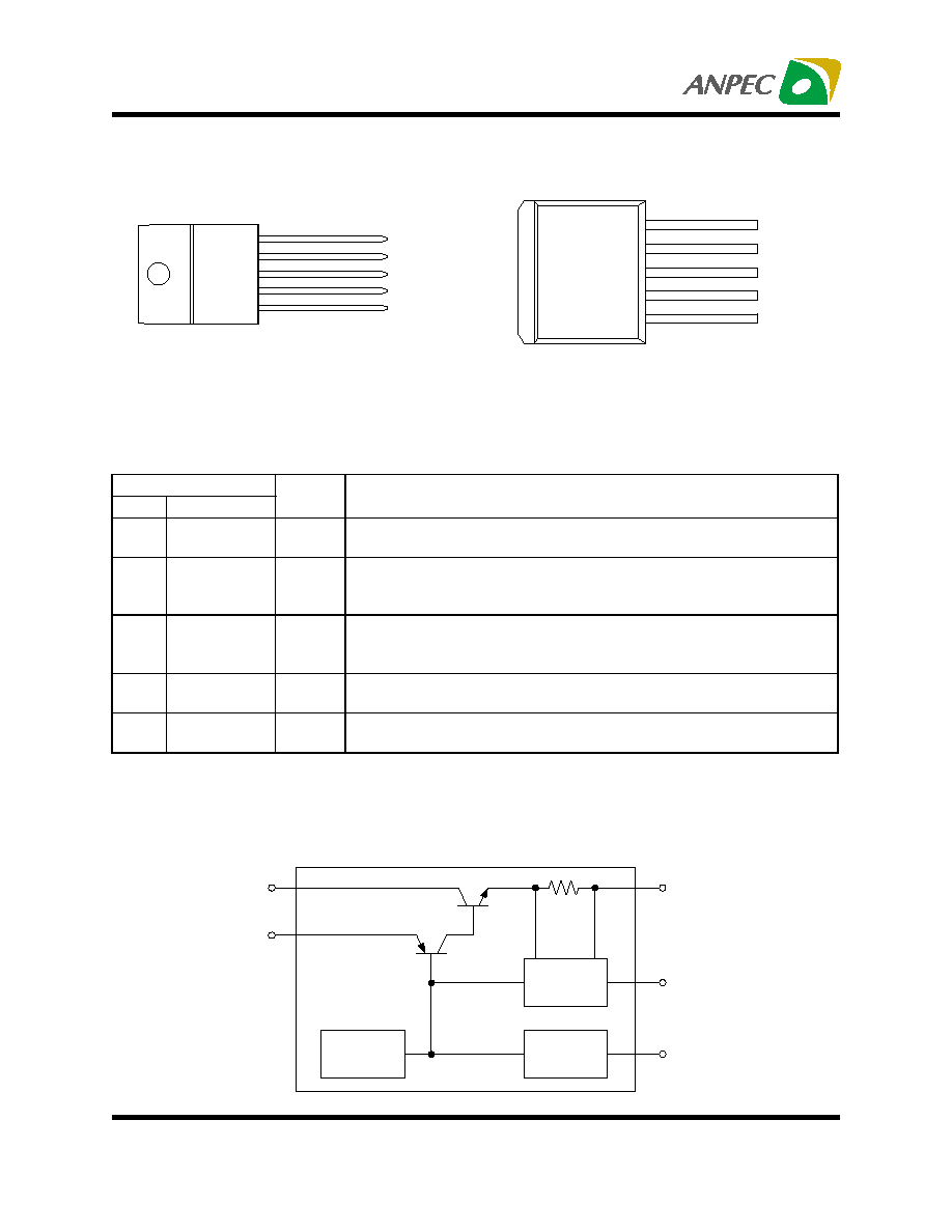
Block Diagram
Pin Configuration
Pin Description
Current
Limit
Voltage
Regulation
Thermal
Protection
V
IN
V
CONTROL
V
OUT
ADJ
V
SENSE
PIN
No.
Name
I/O
Description
1
V
SENSE
I
Positive side of the reference voltage, which allows remote sensing to
obtain excellent load regulation.
2
ADJ
O
Negative side of the reference voltage, which allows to use resistor
divider to set an expect output voltage. A small bypass capacitor can be
connected from this pin to ground to improve PSRR performance.
3
V
OUT
O
Output pin of the regulator, which connects to the TAB. A minimum of
10
µ
F capacitor must be connected from this pin to ground to ensure the
stability.
4
V
CONTROL
I
Supply pin of the control circuitry, which must be always higher than
V
OUT
for the device to regulate. (see electrical characteristics)
5
V
IN
I
Power input pin of the regulator, which must be always higher than
V
OUT
for the device to regulate. (see electrical characteristics)
V
SENSE
ADJ
V
OUT
V
CONTROL
V
IN
1
2
3
4
5
V
SENSE
ADJ
V
OUT
V
CONTROL
V
IN
1
2
3
4
5
Front View of TO-220-5
Front View of TO-252-5/TO-263-5
Copyright
ANPEC Electronics Corp.
Rev. A.4 - Apr., 2003
APL1582
www.anpec.com.tw
3
S ym b ol
Param eter
R atin g
U nit
V
IN
Input Voltage
7
V
V
C O N TR O L
C ontrol Voltage
13.2
V
Q
JA
T herm al R esistance ≠ Ju nction to A m bient
62.5
∞
C / W
P
D
Power D issipation
Internally Lim ited
W
T
J
O perating Junction Tem perature
∞
C
C ontrol S ection
0 to 125
Pow er Transistor
0 to 150
T
STG
Stora ge Tem perature R ange
-65 to +150
∞
C
T
L
Lead Tem perature (Soldering, 10 second)
260
∞
C
Absolute Maximum Ratings
Electrical Characteristics
Unless otherwise noted these specifications apply over , C
IN
=1uF , C
OUT
=10uF , T
J
=0 to 125∞C. Typical values
refer to T
J
=25∞C. V
OUT
=V
SENSE
.
APL1582
Symbol
Parameter
Test Conditions
MIN TYP MAX
UNIT
V
REF
Reference Voltage
V
CONTROL
=2.75 to 12V , V
IN
=2.05V to
5.5V , I
O
=10mA to 3A , V
ADJ
=0V
1.225 1.250 1.275
V
REG
LINE
Line Regulation
V
CONTROL
=2.75V to 12V , V
IN
=1.75V to
5.5V , I
O
=10mA , V
ADJ
=0V
3
mV
REG
LOAD
Load Regulation (note 1)
V
CONTROL
=2.75V , V
IN
=2.1V , I
O
=10mA to
3A , V
ADJ
=0V
5
mV
V
CONTROL
-V
OUT
Dropout Voltage (note 2) V
IN
=2.05V , I
O
=3A , V
ADJ
=0V
1.10 1.25
V
V
IN
-V
OUT
Dropout Voltage (note 2) V
CONTROL
=2.75V , I
O
=3A , V
ADJ
=0V
0.45
V
I
LIMIT
Current Limit
V
CONTROL
=2.75V , V
IN
=2.05V
3.2
A
I
LMIN
Minimum Load Current
(note 3)
V
CONTROL
=5V , V
IN
=3.3V , V
ADJ
=0V
5
10
mA
REG
THERMAL
Thermal Regulation
30mS Pulse
0.01
%
/W
PSRR
Power Supply Ripple
Rejection
T
J
=25
∞
C , V
RIPPLE
=1V
PP
at 120Hz,
V
CONTROL
=5V , V
IN
=5V , I
O
=3A , V
ADJ
=0V
60
70
dB
I
CONTROL
Control Pin Current
V
CONTROL
=2.75V , V
IN
=2.05V , I
O
=3A ,
V
ADJ
=0V
33
120
mA
I
ADJ
Adjust Pin Current
V
CONTROL
=2.75V , V
IN
=2.05V , V
ADJ
=0V
50
120
µ
A
Copyright
ANPEC Electronics Corp.
Rev. A.4 - Apr., 2003
APL1582
www.anpec.com.tw
4
Electrical Characteristics Cont.
Note 1 : Low duty cycle pulse test with Kelvin con-
nections are required to maintain data accuracy .
Note 2 : Drop-out voltage is defined as the minimum
difference between V
IN
and V
OUT
required to maintain
1% V
OUT
regulation .
Note 3 : Minimum load current is defined as the mini-
mum current required at the output to maintain V
OUT
regulation.
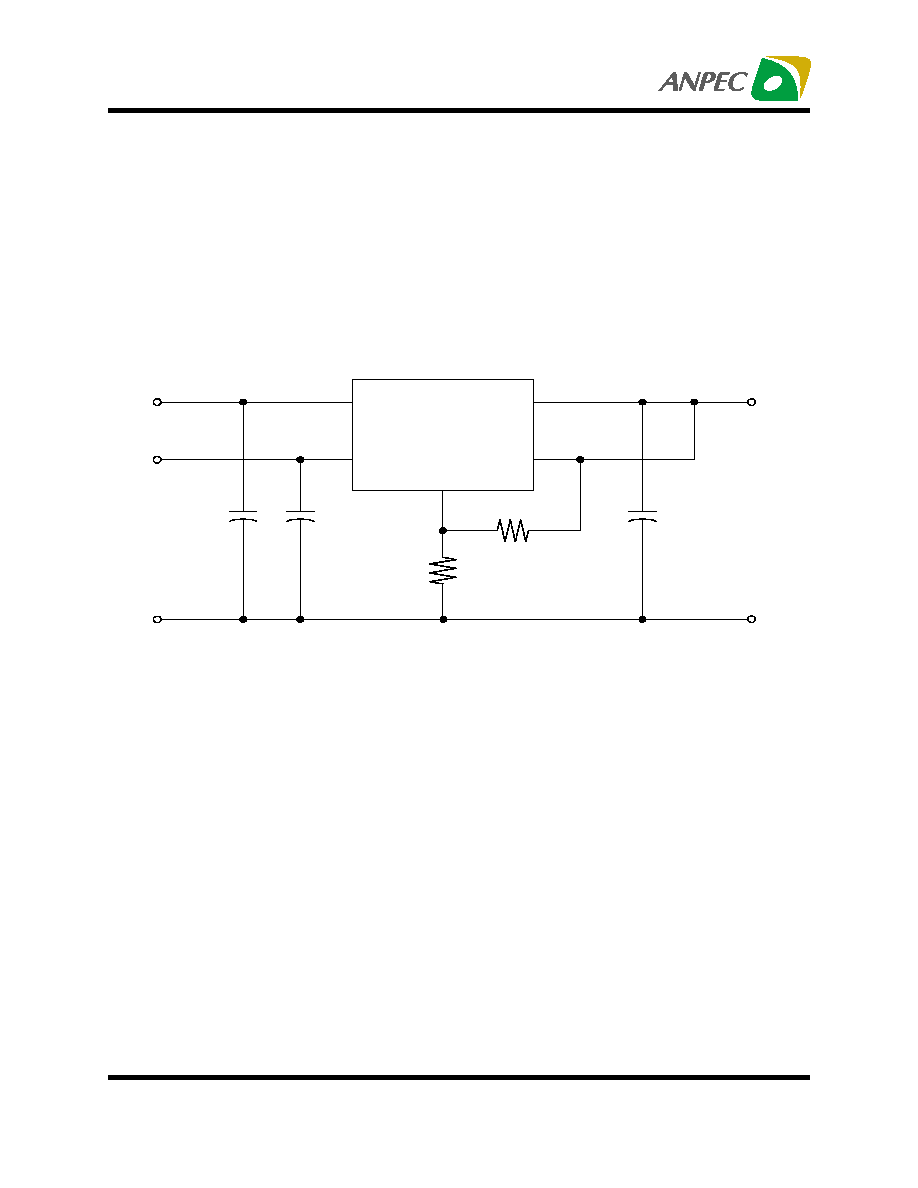
Application Circuit
V
OUT
= V
REF
( 1+ R2 / R1 ) + I
ADJ
* R2
R1 is typically in range of 100
to 125
to satisfy the minimum load current requirement
V
SENSE
V
OUT
V
IN
APL1582
ADJ
V
CONTROL
GND
2.5V
GND
5.0V
3.3V
5
4
2
1
3
R2
125
R1
125
V
REF
-
+
Copyright
ANPEC Electronics Corp.
Rev. A.4 - Apr., 2003
APL1582
www.anpec.com.tw
5
0
100
200
300
400
500
600
700
0
0.5
1
1.5
2
2.5
3
1.225
1.230
1.235
1.240
1.245
1.250
1.255
1.260
1.265
1.270
1.275
-50
-25
0
25
50
75
100 125 150
0
10
20
30
40
50
60
70
80
-50
-25
0
25
50
75
100
125
150
0.0
0.2
0.4
0.6
0.8
1.0
1.2
-50
-25
0
25
50
75
100
125
150
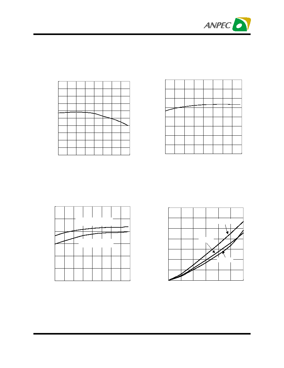
Typical Characteristics
Reference Voltage vs. Junction Temperature
Junction Temperature (∞C)
Reference V
oltage (V)
Adjust Pin Curret vs. Junction Temperature
Junction Temperature (∞C)
Adjust Pin Current (
µ
A)
Minimum Load Current vs. Junction Temperature
Junction Temperature (
∞
C)
V
IN
-V
OUT
Dropout Voltage vs. Output Current
Output Current (A)
V
IN
-V
OUT
Dropout V
oltage (mV)
T
J
=125∞C
V
CONTROL
-V
OUT
=10.75V
Minimum Load Current (mA)
V
CONTROL
-V
OUT
=1.45V
T
J
=25∞C
T
J
=-50∞C
Copyright
ANPEC Electronics Corp.
Rev. A.4 - Apr., 2003
APL1582
www.anpec.com.tw
6
0.7
0.8
0.9
1.0
1.1
1.2
1.3
1.4
0
0.5
1
1.5
2
2.5
3
0
10
20
30
40
50
60
70
0
0 .5
1
1 .5
2
2 .5
3
0
5
10
15
20
25
30
35
40
0
0.5
1
1.5
2
2.5
3
0
1
2
3
4
5
6
7
8
9
-50
-25
0
25
50
75
100
125
150
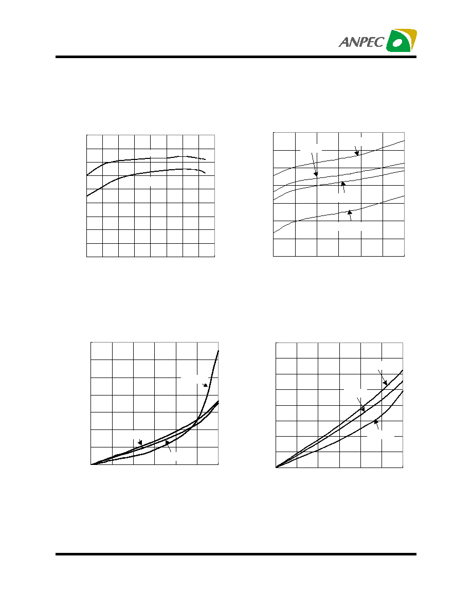
Typical Characteristics (Cont.)
Short-Circuit Current vs. Junction Temperature
Junction Temperature (∞C)
Short-Circuit Current (A)
V
CONTROL
-V
OUT
Dropout Voltage vs. Output Current
Output Currnet (A)
Output Current (A)
Control Pin Current vs. Output Current
Output Current (A)
Control Pin Current (mA)
Control Pin Current (mA)
V
CONTROL
-V
OUT
Dropout V
oltage (mV)
V
IN
=5.0V
V
IN
=3.3V
T
J
=-50∞C
T
J
=0∞C
T
J
=25∞C
T
J
=125∞C
T
J
=0∞C
T
J
=25∞C
T
J
=125∞C
T
J
=0∞C
T
J
=25∞C
T
J
=125∞C
V
IN
-V
OUT
=0.6V
Control Pin Current vs. Output Current
V
IN
-V
OUT
=0.8V
Copyright
ANPEC Electronics Corp.
Rev. A.4 - Apr., 2003
APL1582
www.anpec.com.tw
7
0
5
10
15
20
25
30
35
40
0
0.5
1
1.5
2
2.5
3
0
5
10
15
20
25
30
35
40
0
0.5
1
1.5
2
2.5
3
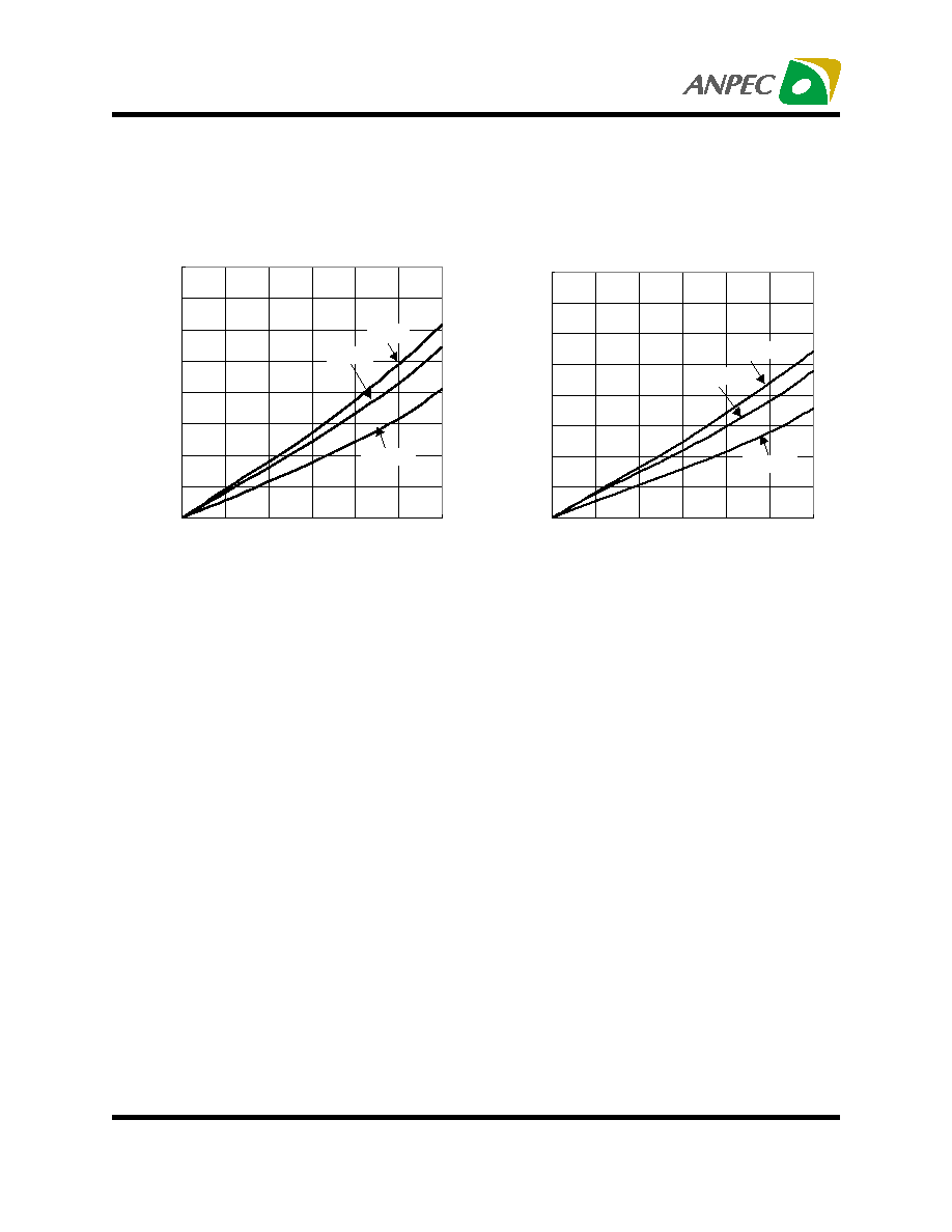
Typical Characteristics (Cont.)
Control Pin Current vs. Output Current
Output Current (A)
Control Pin Current vs. Output Current
Output Current (A)
Control Pin Current (mA)
Control Pin Current (mA)
T
J
=0∞C
T
J
=25∞C
T
J
=125∞C
T
J
=0∞C
T
J
=25∞C
T
J
=125∞C
V
IN
-V
OUT
=1.0V
V
IN
-V
OUT
=4.25V
Copyright
ANPEC Electronics Corp.
Rev. A.4 - Apr., 2003
APL1582
www.anpec.com.tw
8
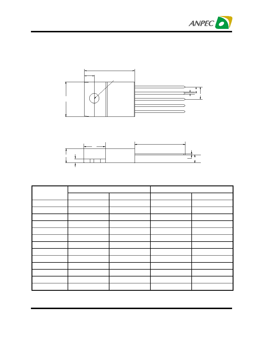
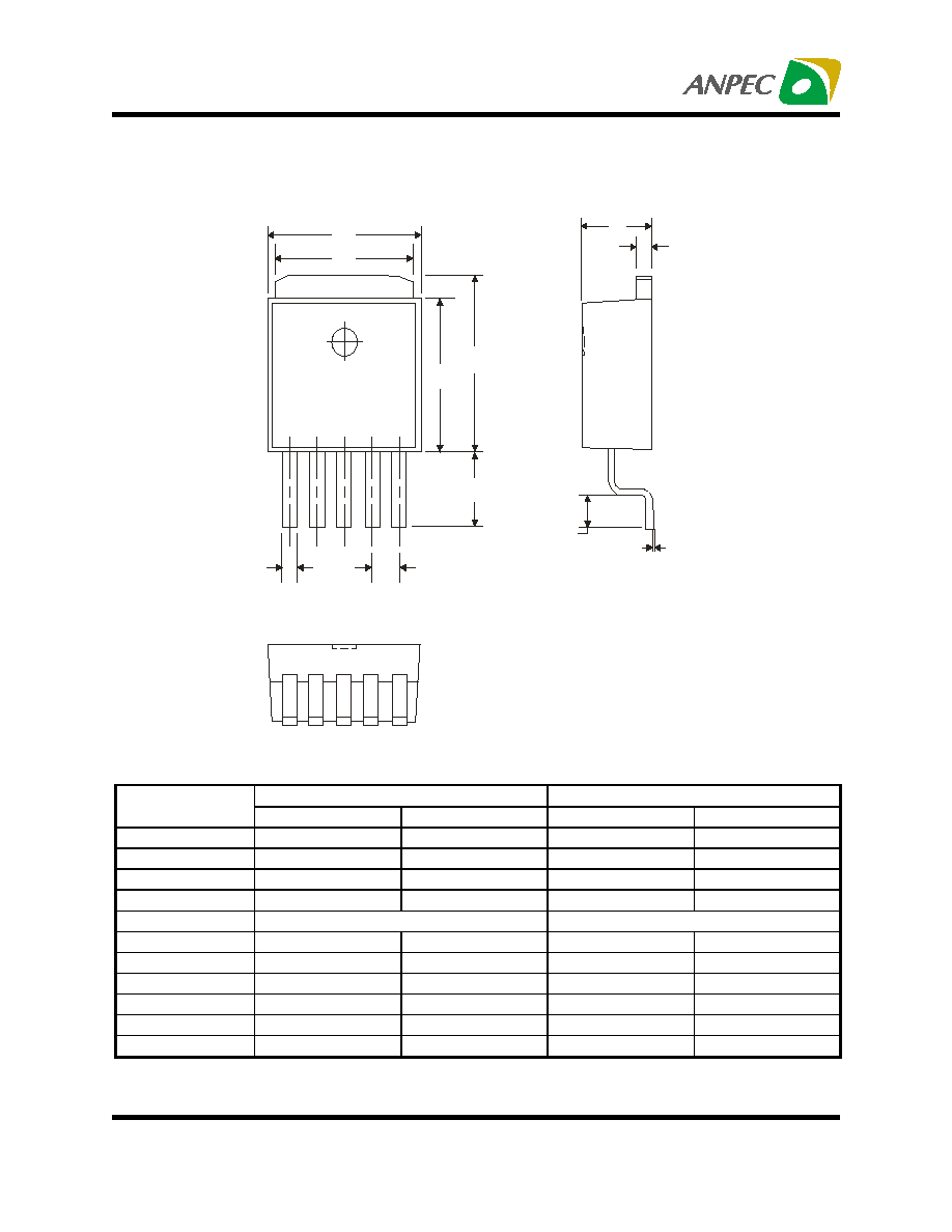
Q
D
R
E
e
b
e1
F
A
c
H1
J1
L
M illimet ers
Inches
Dim
M in.
M ax.
M in.
M ax.
A
3.55
4.83
1.140
0.190
b
0.63
1.02
0.025
0.040
c
0.35
0.56
0.014
0.022
D
14.22
16.51
0.560
0.650
e
1.57
1.83
0.062
0.072
e1
6.68
6.94
0.263
0.273
E
9.65
10.67
0.380
0.420
F
1.14
1.40
0.045
0.055
H1
5.84
6.60
0.230
0.260
J1
2.03
3.05
0.080
0.120
L
13.72
14.22
0.540
0.560
R
3.53
4.09
0.139
0.161
Q
2.54
3.43
0.100
0.135
Package Information
TO-220-5
Copyright
ANPEC Electronics Corp.
Rev. A.4 - Apr., 2003
APL1582
www.anpec.com.tw
9
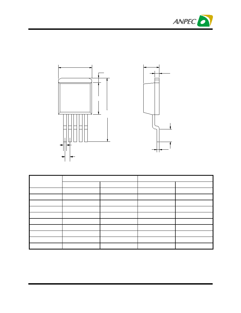
Package Information
TO-252-5
Millimeters
Inches
Dim
Min.
Max.
Min.
Max.
A
6.40
6.80
0.25
0.26
B
5.20
5.50
0.20
0.21
C
6.80
7.20
0.26
0.27
D
2.20
2.80
0.08
0.11
P
1.27 REF
0.05 REF
S
0.50
0.80
0.02
0.03
H
2.20
2.40
0.08
0.09
J
0.45
0.55
0.01
0.02
K
0
0.15
0
0.006
L
0.90
1.50
0.03
0.06
M
5.40
5.80
0.21
0.22
L
K
J
H
B
A
C
M
D
P
S
Copyright
ANPEC Electronics Corp.
Rev. A.4 - Apr., 2003
APL1582
www.anpec.com.tw
10
Package Information
TO-263-5
A
c1
E
D
L
L2
b1
b
c
L1
M illimet er s
Inch es
Dim
M in .
M ax.
M in .
M ax.
A
4.06
4.83
0.160
0.190
b
0.50
0.99
0.020
0.039
b1
1.52
1.83
0.060
0.072
c
0.457
0.736
0.018
0.029
c1
1.14
1.40
0.045
0.055
D
8.25
9.66
0.325
0.380
E
9.65
10.29
0.380
0.405
L
14.60
15.88
0.575
0.625
L1
2.28
2.80
0.090
0.11 0
L2
1.40
0.055
Copyright
ANPEC Electronics Corp.
Rev. A.4 - Apr., 2003
APL1582
www.anpec.com.tw
11
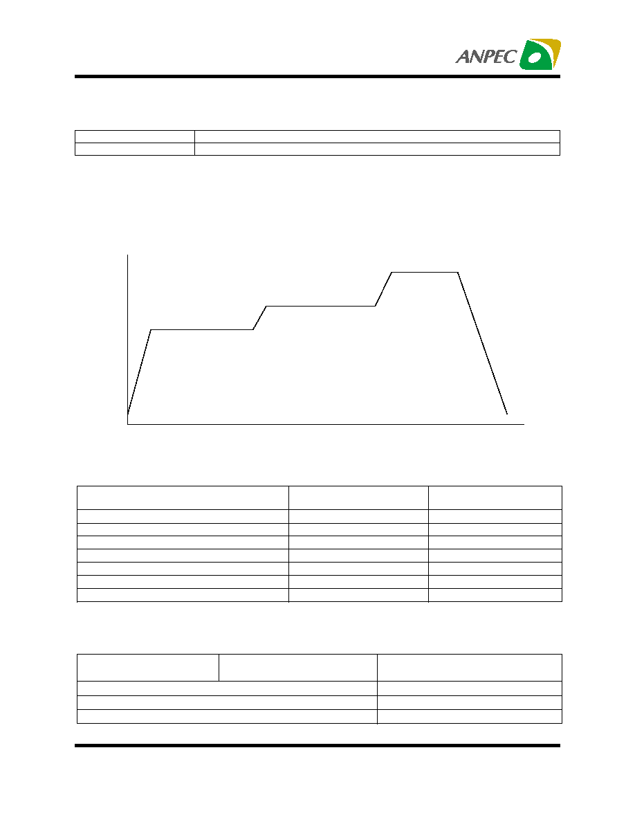
Reference JEDEC Standard J-STD-020A APRIL 1999
Reflow Condition
(IR/Convection or VPR Reflow)
Physical Specifications
Pre-heat temperature
183 C
Peak temperature
Time
∞
temperature
Convection or IR/
Convection
VPR
Average ramp-up rate(183
∞
C to Peak)
3
∞
C/second max.
10
∞
C /second max.
Preheat temperature 125
±
25
∞
C)
120 seconds max.
Temperature maintained above 183
∞
C
60 ~ 150 seconds
Time within 5
∞
C of actual peak temperature
10 ~ 20 seconds
60 seconds
Peak temperature range
220 +5/-0
∞
C or 235 +5/-0
∞
C
215~ 219
∞
C or 235 +5/-0
∞
C
Ramp-down rate
6
∞
C /second max.
10
∞
C /second max.
Time 25
∞
C to peak temperature
6 minutes max.
pkg. thickness
2.5mm
and all bags
pkg. thickness < 2.5mm and
pkg. volume
350 mm
pkg. thickness < 2.5mm and pkg.
volume <
Convection 220 +5/-0
∞
C
Convection 235 +5/-0
∞
C
VPR 215-219
∞
C
VPR 235 +5/-0
∞
C
IR/Convection 220 +5/-0
∞
C
IR/Convection 235 +5/-0
∞
C
Classification Reflow Profiles
Terminal Material
Solder-Plated Copper (Solder Material : 90/10 or 63/37 SnPb).
Lead Solderability
Meets EIA Specification RSI86-91, ANSI/J-STD-002 Category 3.
Copyright
ANPEC Electronics Corp.
Rev. A.4 - Apr., 2003
APL1582
www.anpec.com.tw
12
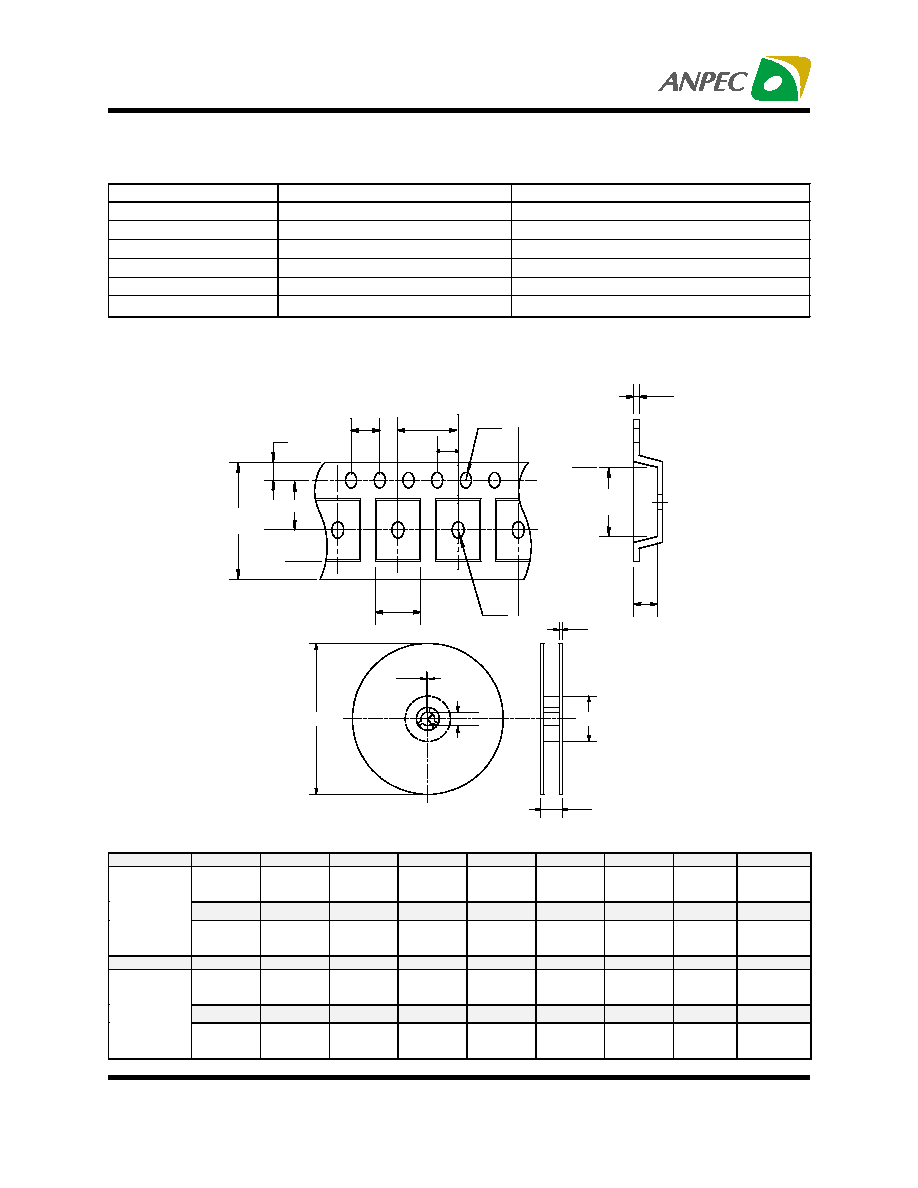
Reliability test program
Test item
Method
Description
SOLDERABILITY
MIL-STD-883D-2003
245
∞
C , 5 SEC
HOLT
MIL-STD-883D-1005.7
1000 Hrs Bias @ 125
∞
C
PCT
JESD-22-B, A102
168 Hrs, 100 % RH , 121
∞
C
TST
MIL-STD-883D-1011.9
-65
∞
C ~ 150
∞
C, 200 Cycles
ESD
MIL-STD-883D-3015.7
VHBM > 2KV, VMM > 200V
Latch-Up
JESD 78
10ms , I
tr
> 100mA
Application
A
B
C
J
T1
T2
W
P
E
330
±
3
100
±
2
13
±
0. 5
2
±
0.5
16.4 + 0.3
-0.2
2.5
±
0.5
16+ 0.3
- 0.1
8
±
0.1
1.75
±
0.1
F
D
D1
Po
P1
Ao
Bo
Ko
t
TO-252
7.5
±
0.1
1.5 +0.1 1.5
±
0.25 4.0
±
0.1
2.0
±
0.1
6.8
±
0.1 10.4
±
0.1 2.5
±
0.1
0.3
±
0.05
Application
A
B
C
J
T1
T2
W
P
E
380
±
3
80
±
2
13
±
0. 5
2
±
0.5
24
±
4
2
±
0.3
24 + 0.3
- 0.1
16
±
0.1 1.75
±
0.1
F
D
D1
Po
P1
Ao
Bo
Ko
t
TO-263
11.5
±
0.1 1.5 +0.1 1.5
±
0.25 4.0
±
0.1
2.0
±
0.1 10.8
±
0.1 16.1
±
0.1 5.2
±
0.1 0.35
±
0.013
(mm)
A
J
B
T2
T1
C
t
Ao
E
W
Po
P
Ko
Bo
D1
D
F
P1
Carrier Tape & Reel Dimension
Copyright
ANPEC Electronics Corp.
Rev. A.4 - Apr., 2003
APL1582
www.anpec.com.tw
13
Customer Service
Anpec Electronics Corp.
Head Office :
5F, No. 2 Li-Hsin Road, SBIP,
Hsin-Chu, Taiwan, R.O.C.
Tel : 886-3-5642000
Fax : 886-3-5642050
Taipei Branch :
7F, No. 137, Lane 235, Pac Chiao Rd.,
Hsin Tien City, Taipei Hsien, Taiwan, R. O. C.
Tel : 886-2-89191368
Fax : 886-2-89191369
Cover Tape Dimensions
Application
Carrier Width
Cover Tape Width
Devices Per Reel
TO- 252
16
13.3
2500
TO- 263
24
21.3
1000