 | –≠–ª–µ–∫—Ç—Ä–æ–Ω–Ω—ã–π –∫–æ–º–ø–æ–Ω–µ–Ω—Ç: APL5331 | –°–∫–∞—á–∞—Ç—å:  PDF PDF  ZIP ZIP |
3A Bus Termination Regulator
Copyright
ANPEC Electronics Corp.
Rev. A.8 - Oct., 2003
APL5331
www.anpec.com.tw
1
ANPEC reserves the right to make changes to improve reliability or manufacturability without notice, and advise
customers to obtain the latest version of relevant information to verify before placing orders.
∑∑
∑∑
∑
Provide Bi-direction Current
- Sourcing or Sinking Current up to 3A
∑∑
∑∑
∑
1.25V/0.9V Output for DDR I/II Applications
∑∑
∑∑
∑
Fast Transient Response
∑∑
∑∑
∑
High Output Accuracy
- ±20mV over Load, VOUT Offset and
Temperature
∑∑
∑∑
∑
Adjustable Output Voltage by External Resistors
∑∑
∑∑
∑
Current-Limit Protection
∑∑
∑∑
∑
On-Chip Thermal Shutdown
∑∑
∑∑
∑
Shutdown for Standby or Suspend Mode
∑∑
∑∑
∑
Simple SOP-8, SOP-8-P with thermal pad,
TO-252- 5 and TO-263-5 Packages
Features
General Description (Cont.)
On-chip thermal shutdown provides protection against
any combination of overload that would create ex-
cessive junction temperature. The output voltage of
APL5331 track the voltage at VREF pin. A resistor
divider connected to VIN, GND and VREF pins is
used to provide a half voltage of VIN to VREF pin. In
addition, an external ceramic capacitor and an open-
drain transistor connected to VREF pin provides soft-
start and shutdown control respectively. Pulling and
holding the VREF to GND shuts off the output. The
output of APL5331 will be high impedance after be-
ing shut down by VREF or thermal shutdown function.
Applications
∑
DDR I/II SDRAM Termination
∑
SSTL-2/3 Termination Voltage
∑
Applications Requiring the Regulator with
Bi-direction 3A Current Capability
Pin Configuration
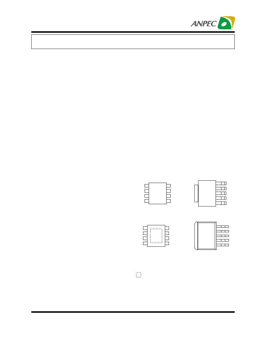
TO-252-5 (Top View)
VOUT
VREF
VCNTL
GND
VIN
12
3
4
5
TAB is VCNTL
TO-263-5 (Top
View)
VIN
GND
VCNTL
VREF
VOUT
1
2
3
4
5
TAB is VCNTL
SOP-8 (Top View)
1
2
3
4
5
6
7
8
VIN
GND
VREF
VOUT
VCNTL
VCNTL
VCNTL
VCNTL
General Description
The APL5331 linear regulator is designed to provide
a regulated voltage with bi-directional output current
for DDR-SDRAM termination. The APL5331 integrates
two power transistors to source or sink current up to
3A. It also incorporate current-limit, thermal shut-
down and shutdown control functions into a single
chip. Current-limit circuit limits the short-circuit
current.
1
2
3
4
5
6
7
8
VIN
GND
VREF
VOUT
NC
VCNTL
NC
NC
SOP-8-P (Top View)
= Thermal Pad
NC = No internal connection
(connected to GND plane for better heat
dissipation)

Copyright
ANPEC Electronics Corp.
Rev. A.8 - Oct., 2003
APL5331
www.anpec.com.tw
2
P a c k a g e C o d e
K : S O P -8 K A : S O P -8 -P
U 5 : T O -2 5 2 -5 G 5 : T O -2 6 3 -5
T e m p . R a n g e
C : 0 to 7 0
o
C
H a n d lin g C o d e
T R : T a p e & R e e l
L e a d F re e C o d e
L : L e a d F re e D e v ic e B la n k : O rg in a l D e v ic e
A P L 5 3 3 1
H a n d lin g C o d e
T e m p . R a n g e
P a c k a g e C o d e
A P L 5 3 3 1
X X X X X
A P L 5 3 3 1 K C -T R :
A P L 5 3 3 1 K A C -T R :
X X X X X - D a te C o d e
A P L 5 3 3 1
X X X X X
A P L 5 3 3 1 U 5 C -T R :
A P L 5 3 3 1 G 5 C -T R :
X X X X X - D a te C o d e
L e a d F re e C o d e
Ordering and Marking Information
Pin Description
PIN NAME
I/O
DESCRIPTION
VIN I
Main power input pin. Connect this pin to a voltage source and an input
capacitor. The APL5331 sources current to VOUT pin by controlling the upper
NPN pass transistor, providing a current path from VIN pin.
GND O
Power and signal ground. Connect this pin to system ground plane with shortest
traces. The APL5331 sinks current from VOUT pin by controlling the lower NPN
pass transistor, providing a current path to GND pin. This pin is also the ground
path for internal control circuitry.
VCNTL I
Power input pin for internal control circuitry. Connect this pin to a voltage source,
providing a bias for the internal control circuitry. A bypass capacitor is usually
connected near this pin.
VREF I
Reference voltage input and active-low shutdown control pin. Apply a voltage to
this pin as a reference voltage for the APL5331. Connect this pin to a resistor
divider, between VIN and GND, and a capacitor for soft-start and filtering noise
purposes. Applying and holding this pin low by an open-drain transistor to shut
down the output.
VOUT O
Output pin of the regulator. Connect this pin to load. Output capacitors
connected this pin improves stability and transient response. The output voltage
tracks the reference voltage and is capable of sourcing or sinking current up to
3A.
Block Diagram
G ND
V O U T
V IN
V C N TL
V RE F
C u rren t
L im it
The rm a l
L im it
V o lta g e
R e gu la t io n
S h ut d ow n

Copyright
ANPEC Electronics Corp.
Rev. A.8 - Oct., 2003
APL5331
www.anpec.com.tw
3
Symbol Parameter
Range
Unit
V
CNTL
VCNTL Supply Voltage
3.1 ~ 6V
V
V
IN
VIN Supply Voltage
1.6 ~ 3.5
V
V
REF
VREF Input Voltage
0.8 ~ 1.75
V
I
OUT
VOUT Output Current (Note1, 2)
-3 ~ +3
A
T
J
Junction Temperature
0 ~ 125
o
C
Symbol Parameter
Rating
Unit
V
CNTL
VCNTL Supply Voltage, VCNTL to GND
-0.2 ~ 7
V
V
IN
VIN Supply Voltage, VIN to GND
-0.2 ~ 3.9
V
P
D
Power Dissipation
Internally Limited
W
T
J
Junction Temperature
150
o
C
T
STG
Storage Temperature
-65 ~ 150
o
C
T
SDR
Soldering Temperature, 10 Seconds
300
o
C
V
ESD
Minimum ESD Rating (Human Body Mode)
±
3
kV
Note1 : The symbol "+" means the VOUT sources current to load; the symbol "-" means the VOUT sinks
current to GND.
Note2 : The max. I
OUT
varies with the T
J
. Please refer to the typical characteristics.
Absolute Maximum Ratings
Thermal Characteristics
Symbol
Parameter
Rating
Unit
JA
Thermal Resistance in Free Air
SOP-8
SOP-8-P
TO-252-5
TO-263-5
160
80
80
50
∞C/W
Recommended Operating Conditions

Copyright
ANPEC Electronics Corp.
Rev. A.8 - Oct., 2003
APL5331
www.anpec.com.tw
4
Electrical Characteristics
Refer to the typical application circuit. These specifications apply over, V
CNTL
=3.3V, V
IN
=2.5V/1.8V,
V
REF
=0.5V
IN
and T
J
= 0 to 125∞C, unless otherwise specified. Typical values refer to T
J
=25∞C.
APL5331
Symbol
Parameter Test
Conditions
M in Typ M ax
Unit
Output Voltage
V
OUT
VOUT Output Voltage
I
OUT
=0A
V
REF
V
System Accuracy
Over tem perature, VOUT offset, and
load regulation
-20 20
m V
I
OUT
=+10m A -14
-9
V
OS
VOUT Offset Voltage
(V
OUT
≠V
REF
)
I
OUT
=-10m A
2
8
m V
I
OUT
=+10m A to +3A
-6
-3
Load Regulation
I
OUT
= -10m A to -3A
7
12
m V
Protection
Sourcing Current T
J
=25∞C
(V
IN
=2.5V) T
J
=125∞C
+3.3 +3.6
+3.1
Sinking Current T
J
=25∞C
(V
IN
=2.5V) T
J
=125∞C
-3.3 -3.6
-3.1
Sourcing Current T
J
=25∞C
(V
IN
=1.8V) T
J
=125∞C
+2.9 +3.2
+2.6
I
LIM
Current Lim it
Sinking Current T
J
=25∞C
(V
IN
=1.8V) T
J
=125∞C
-2.9 -3.2
-2.6
A
T
SD
Therm al Shutdown
Tem perature
Rising T
J
150
o
C
Therm al Shutdown Hysteresis
40
o
C
Input Current
I
OUT
=0A 2
4.5
6
I
OUT
=
±
3A (Norm al Operation),
V
CNTL
=5V
50 110
I
CNTL
VCNTL Supply Current
V
REF
=GND (Shutdown)
2.6
m A
V
REF
=1.25V/0.9V (Norm al Operation)
150 500 nA
I
VREF
VREF Bias Current
(The current flows out of VREF) V
REF
=GND (Shutdown)
20
40
µ
A
Shutdow n Control
Shutdown Threshold Voltage
0.2 0.35 0.65 V
Copyright
ANPEC Electronics Corp.
Rev. A.8 - Oct., 2003
APL5331
www.anpec.com.tw
5
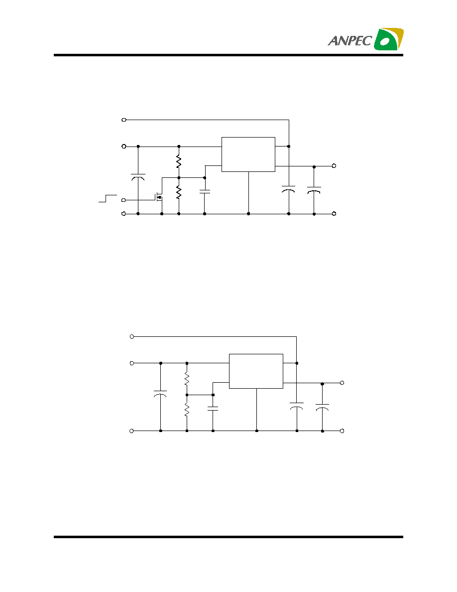
Typical Application Circuit
C
OUT
: 470
µ
F, ESR=25m
R
1
, R2 : 1k
, 1%
Q1 : APM2300 AC
V
C N TL
+3.3V
C
C N TL
47uF
V
OU T
+1.25V/0.9V
-3~+3A
C
SS
0.1uF
GN D
R
1
1k
R
2
1k
V
IN
+2.5V/1.8V
GN D
C
IN
470uF
Q
1
Shutdow n
C
OU T
470uF
V
R EF
G N D
VR EF
VIN
VO U T
VC N TL
Note : Since R
1
and R
2
are very small, the voltage offset
caused by the bias current of VREF can be ignore.
2. V
OUT
=1.4V Application
V
CNT L
+5V
C
CNT L
47
µ
F
V
O UT
+1.4V/
-3~+3A
C
S S
0.1
µ
F
GND
R
1
1k
R
2
1k
V
IN
+2.8V
GND
C
IN
470
µ
F
C
O UT
470
µ
F
V
RE F
GN D
VR EF
VIN
VOU T
VC N TL
1. V
OUT
=1.25V/0.9V Application