
Low I
Q
, Low Dropout 560mA Fixed Voltage Regulator
Copyright
ANPEC Electronics Corp.
Rev. A.6 - Mar., 2004
APL5508/5508R/5509/5509R
www.anpec.com.tw
1
ANPEC reserves the right to make changes to improve reliability or manufacturability without notice, and advise
customers to obtain the latest version of relevant information to verify before placing orders.
SOT-223 (Top View)
APL5509
V
IN
G N D
V
O U T
1
2
3
T A B is G N D
Features
The APL5508/9/R series are micropower, low drop-
out linear regulators, which operate from 2.7V to 6V
input voltage and deliver up to 560mA. Typical drop-
out voltage is only 600mV at 560mA loading. De-
signed for use in battery-powered system, the low
60
µ
A quiescent current makes it an ideal choice.
Design with an internal P-channel MOSFET pass
transistor, the APL5508/9/R maintain a low supply
current, independent of the load current and dropout
voltage. Other features include thermal-shutdown
protection, current limit protection to ensure speci-
fied output current and controlled short-circuit current.
The APL5508/9/R regulators come in a miniature SOT-
23, SOT-89 and SOT-223 packages.
Applications
∑
5V to 3.3~4.3V Linear Regulators
∑
3.3V to 1.5~2.5V Linear Regulators
∑
CD-R/W, DVD Player
∑
LAN Card, ADSL/Cable Modem
∑
Computers
∑∑
∑∑
∑
Low Quiescent Current : 60
µ
A (No load)
∑∑
∑∑
∑
Low Dropout Voltage : 600mV (@560mA)
∑∑
∑∑
∑
Very low Shutdown Current : < 0.5uA
∑∑
∑∑
∑
Fixed Output Voltage : 1.5V ~ 4.5V
by step 0.1V increment
∑∑
∑∑
∑
Stable with 1uF Output Capacitor
∑∑
∑∑
∑
Stable with Aluminum, Tantalum or Ceramic
Capacitors .
∑∑
∑∑
∑
No Protection Diodes Needed
∑∑
∑∑
∑
Built in Thermal Protection
∑∑
∑∑
∑
Built in Current Limit Protection
∑∑
∑∑
∑
Controlled Short Circuit Current : 50mA
∑∑
∑∑
∑
Fast Transient Response
∑∑
∑∑
∑
Short Setting Time
∑∑
∑∑
∑
SOT-23, SOT-89 and SOT-223 Packages
Pin Configuration
General Description
SOT-23 (Top
View)
G ND
1
2
3
V
O U T
V
IN
APL5508
SOT-23 (Top
View)
APL5509
G ND
1
2
3
V
O U T
V
IN
APL5508
SOT-89 (Top View)
G N D
V
IN
V
O UT
1
2
3
T A B is V
IN
APL5509
SOT-89 (Top View)
G N D
V
IN
V
O U T
1
2
3
T A B is G N D
SOT-223 (Top View)
APL5508
V
O U T
V
IN
G N D
1
2
3
T A B is V
IN
SOT-223 (Top View)
APL5509R
V
O U T
G N D
V
IN
1
2
3
T A B is G N D
SOT-223 (Top View)
APL5508R
V
IN
V
O U T
G N D
1
2
3
T A B is V
O U T
Copyright
ANPEC Electronics Corp.
Rev. A.6 - Mar., 2004
APL5508/5508R/5509/5509R
www.anpec.com.tw
2
P a ckage C ode
A : S O T -23 D : S O T -89 V : S O T -223
T e m p . R a nge
C : 0 to 70 C
H andling C ode
T R : T ap e & R eel
V o ltage C ode :
15 : 1 .5V ~ 4 5 : 4.5 V
Lea d F ree D evice
L : L ead F ree D e vice B lan k : O rig ina l D evice
A P L5508/9/R -
H andling C ode
T e m p . R a nge
P a ckage C ode
V o ltage C ode
A P L55 08/9/R
XXXXX 15
XXXXX - D ate C ode ; 1 5 - 1.5V
A P L55 08/9/R -15 D /V :
Lea d F ree C od e
Product
Name
Marking
Product
Name
Marking
Product
Name
Marking
Product
Name
Marking
APL5508-15A
589X
APL5508R-15A 58R9X APL5509-15A
599X
APL5509R-15A 59R9X
APL5508-16A
58AX
APL5508R-16A 58RAX APL5509-16A
59AX
APL5509R-16A 59RAX
APL5508-17A
58BX
APL5508R-17A 58RBX APL5509-17A
59BX
APL5509R-17A 59RBX
APL5508-18A
58CX
APL5508R-18A 58RCX APL5509-18A
59CX
APL5509R-18A 59RCX
APL5508-19A
58DX
APL5508R-19A 58RDX APL5509-19A
59DX
APL5509R-19A 59RDX
APL5508-20A
58EX
APL5508R-20A 58REX APL5509-20A
59EX
APL5509R-20A 59REX
APL5508-21A
58FX
APL5508R-21A 58RFX APL5509-21A
59FX
APL5509R-21A 59RFX
APL5508-22A
58GX
APL5508R-22A 58RGX APL5509-22A
59GX
APL5509R-22A 59RGX
APL5508-23A
58HX
APL5508R-23A 58RHX APL5509-23A
59HX
APL5509R-23A 59RHX
APL5508-24A
58IX
APL5508R-24A
58RIX
APL5509-24A
59IX
APL5509R-24A
59RIX
APL5508-25A
58JX
APL5508R-25A 58RJX
APL5509-25A
59JX
APL5509R-25A 59RJX
APL5508-26A
58KX
APL5508R-26A 58RKX APL5509-26A
59KX
APL5509R-26A 59RKX
APL5508-27A
58LX
APL5508R-27A 58RLX APL5509-27A
59LX
APL5509R-27A 59RLX
APL5508-28A
58MX
APL5508R-28A 58RMX APL5509-28A
59MX
APL5509R-28A 59RMX
APL5508-29A
58NX
APL5508R-29A 58RNX APL5509-29A
59NX
APL5509R-29A 59RNX
APL5508-30A
58OX
APL5508R-30A 58ROX APL5509-30A
59OX
APL5509R-30A 59ROX
APL5508-31A
58PX
APL5508R-31A 58RPX APL5509-31A
59PX
APL5509R-31A 59RPX
APL5508-32A
58QX
APL5508R-32A 58RQX
APL550932A
59QX
APL5509R-32A 59RQX
APL5508-33A
58RX
APL5508R-33A 58RRX APL5509-33A
59RX
APL5509R-33A 59RRX
APL5508-34A
58SX
APL5508R-34A 58RSX APL5509-34 A
59SX
APL5509R-34 A 59RSX
APL5508-35A
58TX
APL5508R-35A 58RTX APL5509-35A
59TX
APL5509R-35A 59RTX
APL5508-43A
58UX
APL5508R-43A 58RUX APL5509-43A
59UX
APL5509R-43A 59RUX
APL5508-45A
58VX
APL5508R-45A 58RVX APL5509-45A
59VX
APL5509R-45A 59RVX
Ordering and Marking Information
∞
Marking Information
SOT-23 package
The last character "X" in the marking is for data code.
Copyright
ANPEC Electronics Corp.
Rev. A.6 - Mar., 2004
APL5508/5508R/5509/5509R
www.anpec.com.tw
3
Symbol Parameter Rating
Unit
V
IN
, V
OUT
Input Voltage or Out Voltage
6.5
V
R
TH,JA
Thermal Resistance ≠ Junction to Ambient
SOT-23 : 260
SOT-89 : 180
SOT-223 : 135
∞C/W
R
TH,JC
Thermal Resistance ≠ Junction to Case
SOT-23 : 130
SOT-89 : 38
SOT-223 : 15
∞C/W
P
D
Power Dissipation
Internally Limited
W
T
J
Operating Junction Temperature
∞C
Control Section
0 to 125
Power Transistor
0 to 150
T
STG
Storage Temperature Range
-65 to +150
∞C
T
L
Lead Temperature (Soldering, 10 second)
260 ∞C
Electrical Characteristics
Unless otherwise noted these specifications apply over full temperature, C
IN
=C
OUT
=1uF, T
J
=0 to 125
∞
C.
Typical values refer to T
J
=25
∞
C.
APL5508/9/R
Symbol Parameter
Test
Conditions
Min. Typ. Max.
Unit
V
IN
Input
Voltage
2.7
6
V
V
OUT
Output
Voltage
V
OUT
+1.0V< V
CC
<6.0V, 0mA< I
OUT
< I
MAX
V
OUT
-2
%
V
OUT
V
OUT
+2
%
V
I
LIMIT
Circuit Current Limit V
IN
=V
OUT
+1V
800 mA
I
SHORT
Short
Current
V
OUT
=0V
50 mA
I
OUT
Load Current
V
IN
=V
OUT
+1V
560
mA
REG
LINE
Line Regulation
V
OUT
+1V< V
CC
<6.0V, I
OUT
=1mA
1
10
mV
REG
LOAD
Load Regulation
V
IN
=V
OUT
+1V, 0mA< I
OUT
< I
MAX
20 40
mV
Load
Transient V
IN
= V
OUT
+1V , I
OUT
=1mA-560mA in 1
µ
s 150
250 mV
PIN
No. Name
I/O Description
1 V
IN
I
Supply voltage input.
2 GND
Ground pins of the circuitry, and all ground pins must be soldered
To PCB with proper power dissipation.
3 V
OUT
O
Output pin of the regulator.
Pin Description
Absolute Maximum Ratings
Copyright
ANPEC Electronics Corp.
Rev. A.6 - Mar., 2004
APL5508/5508R/5509/5509R
www.anpec.com.tw
4
Electrical Characteristics (Cont.)
Unless otherwise noted these specifications apply over full temperature, C
IN
=C
OUT
=1uF, T
J
=0 to 125
∞
C.
Typical values refer to T
J
=25
∞
C.
1
APL5508/9/R
Symbol Parameter
Test
Conditions
Min. Typ. Max.
Unit
1.5V
V
OUT
<2.0V
1.1
1.3
2.0V
V
OUT
<2.5V
0.9
1.0
2.5V
V
OUT
<3V
0.7
0.8
V
DROP
Dropout
Voltage
(Note1)
I
OUT
=560mA
3V
V
OUT
3.5V
0.6
0.7
V
PSRR Ripple Rejection
F
1kHz, 1Vpp at V
IN
= V
OUT
+1.0V
45 55 dB
No load
60 100
I
Q
Quiescent Current
I
OUT
=560mA
450 500
µ
A
OTS Over Temperature
150
∞
C
Over Temperature
Hysteresis
30
∞
C
TC
Output Voltage
Temperature
Coefficient
50
ppm/
∞
C
C
OUT
Output Capacitor
4.7
µ
F
ESR
0.01
0.1
1
Ohm
Note1 : Dropout voltage definition : V
IN
-V
OUT
when V
OUT
is 2% below the value of V
OUT
for V
IN
= V
OUT
+1V
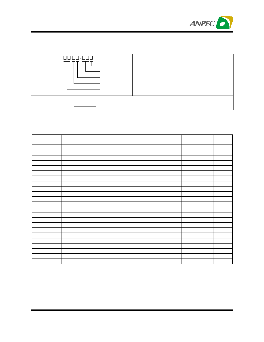
Application Circuit
V
O UT
V
IN
G N D
VO U T
C
IN
1
µ
F
AP L5508/R
AP L5509/R
IN P U T
2.7V to 6V
C
O UT
4.7
µ
F
Copyright
ANPEC Electronics Corp.
Rev. A.6 - Mar., 2004
APL5508/5508R/5509/5509R
www.anpec.com.tw
5
0
0.5
1
1.5
2
2.5
3
3.5
0
1
2
3
4
5
6
0
50
100
150
200
250
300
350
400
450
0
100
200
300
400
500
0
50
100
150
200
250
300
350
400
450
0
1
2
3
4
5
6
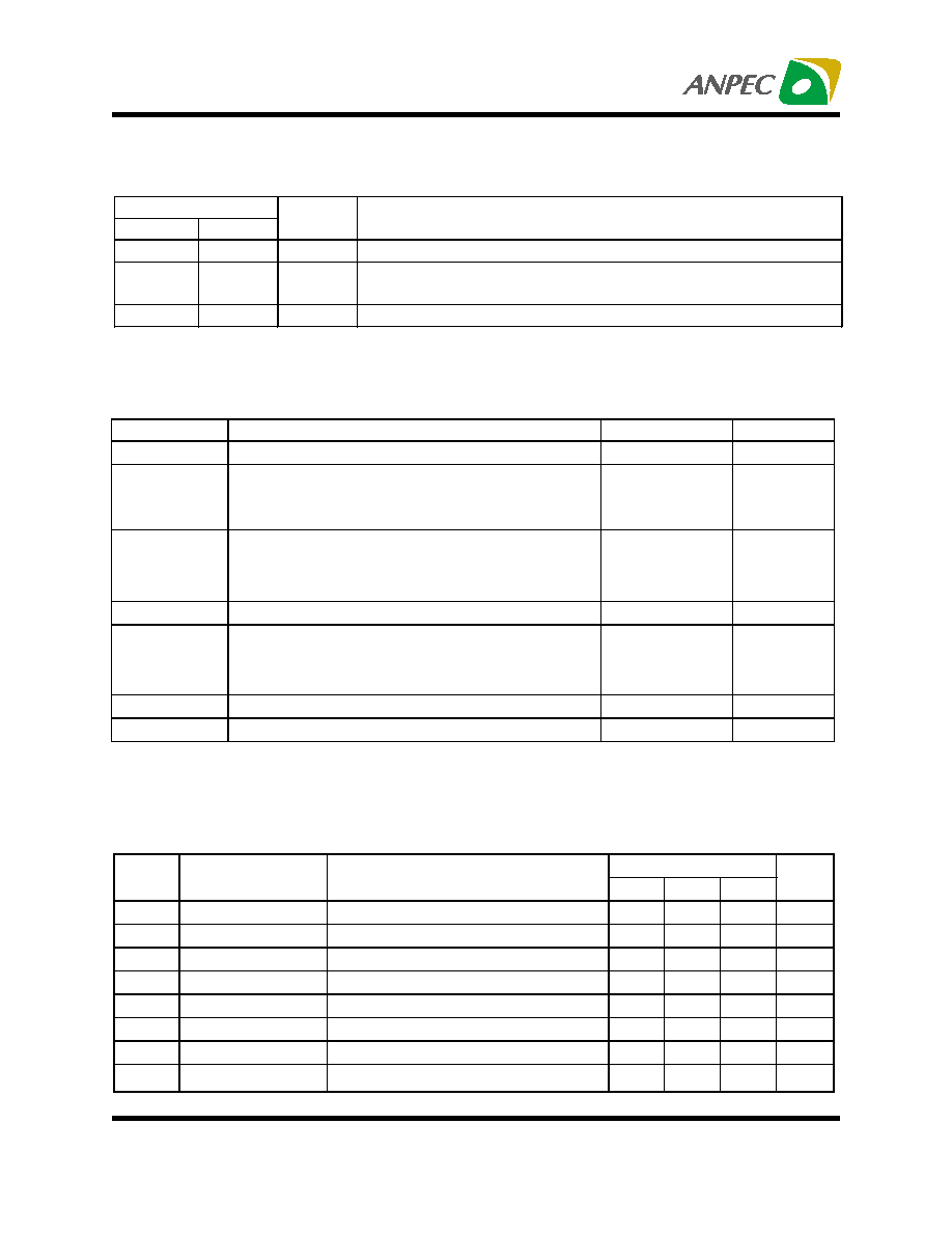
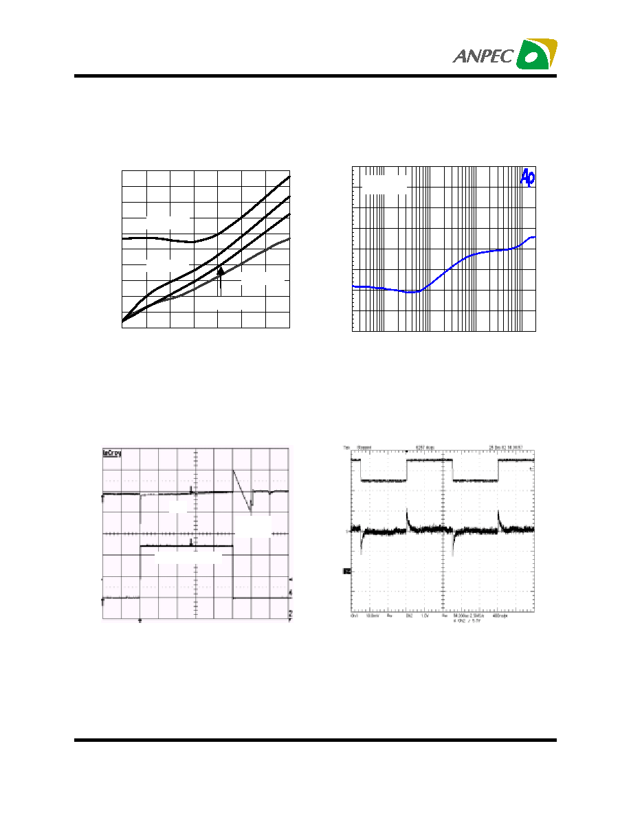
Typical Characteristics
Quiescent Current vs. Input Voltage
Input Voltage (V)
Quiescent Current (
µ
A)
Quiescent Current vs. Output Current
Quiescent Current (
µ
A)
Output Current (mA)
Output Voltage vs. Input Voltage
Input Voltage (V)
Output V
oltage (V)
APL5508/9/R-33
V
IN
=5V
I
OUT
=0mA
APL5508/9/R-33
APL5508/9/R-33
3.28
3.28
3.29
3.29
3.30
3.30
3.31
3.31
-40
-20
0
20
40
60
80
100 120 140
Temperature (∞C )
Output V
oltage (V)
APL5508/9/R-33
Output Voltage vs. Temperature
I
OUT
=0mA
Copyright
ANPEC Electronics Corp.
Rev. A.6 - Mar., 2004
APL5508/5508R/5509/5509R
www.anpec.com.tw
6
0
100
200
300
400
500
600
700
800
900
1000
0
80
160
240
320
400
480
560
-80
+0
-70
-60
-50
-40
-30
-20
-10
20
200 k
50
100
200
500
1 k
2 k
5 k
10 k
20 k
50 k
100 k
Typical Characteristics
PSRR vs. Frequency
Frequency (H
Z
)
PSRR (dB)
v
IN
=5V
I
OUT
=50mA
Output Current (mA)
Dropout V
oltage (mV)
APL5508/9/R-33
Dropout Voltage vs. Output Current
Load-Transient Response
Output V
oltage (200mV/div)
Time (100
µ
s/div)
V
OUT
Time (200
µ
s/div)
Line-Transient Response
V
IN
=4.5V~5.5V
C
OUT
=1
µ
F
I
OUT
=10mA
Output V
oltage (10mV/div)
APL5308/9-33
APL5308/9-33
V
IN
=5V
C
OUT
=1
µ
F
V
OUT
I
OUT
=1mA~560mA
V
OUT
=2.5V
V
OUT
=3.3V
V
OUT
=2.8V
V
OUT
=1.9V
Copyright
ANPEC Electronics Corp.
Rev. A.6 - Mar., 2004
APL5508/5508R/5509/5509R
www.anpec.com.tw
7
0.001
0.01
0.1
1
0
100
200
300
400
500
0.001
0.01
0.1
1
0
100
200
300
400
500
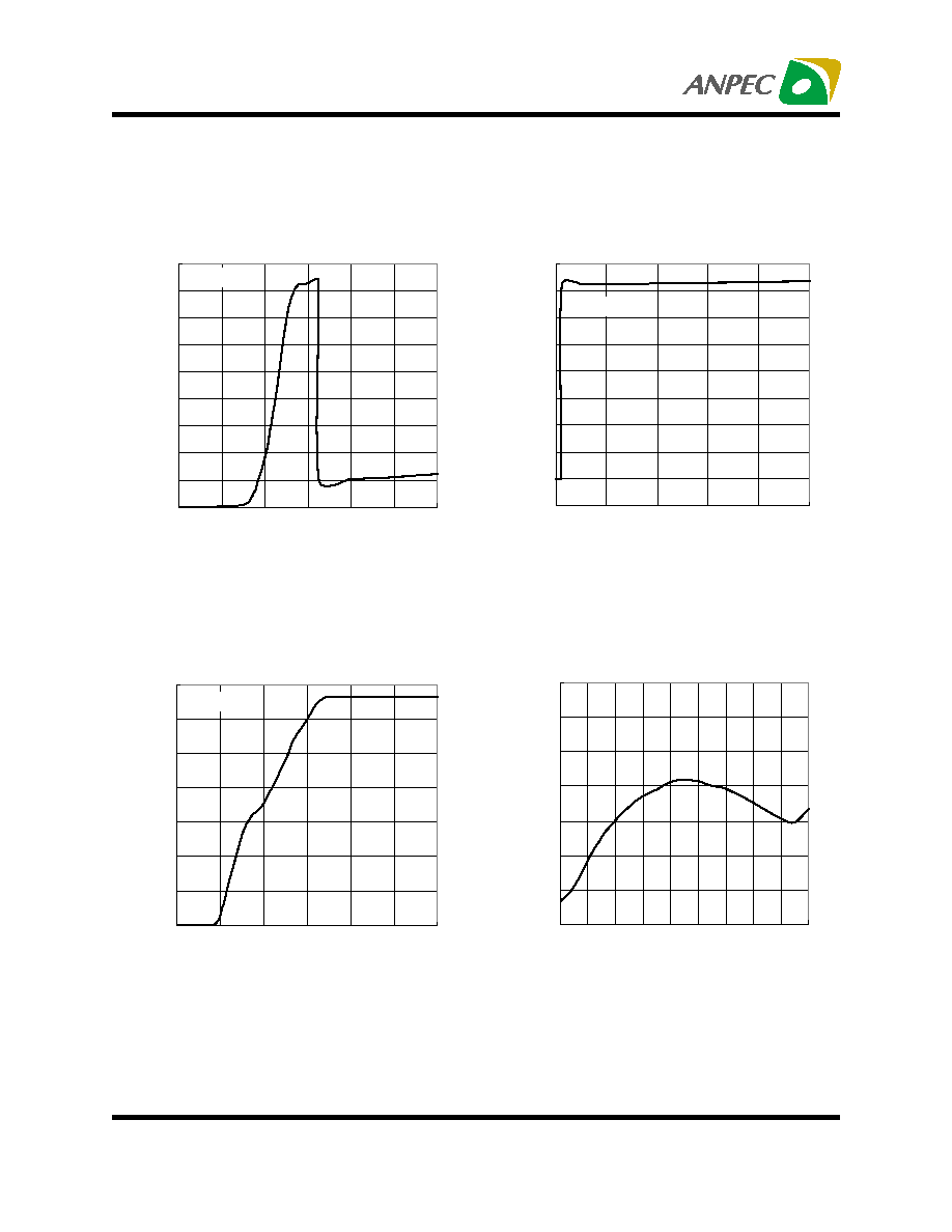
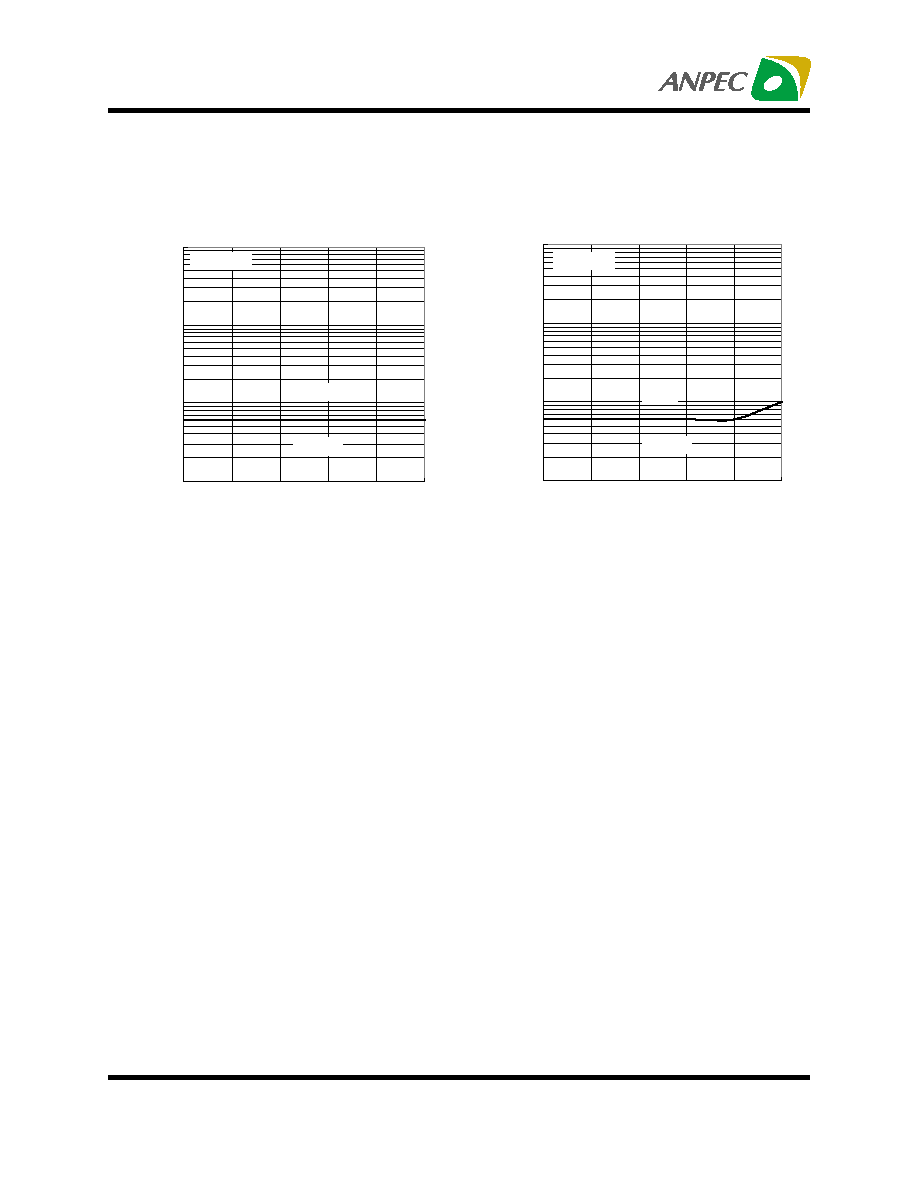
Typical Characteristics
Output Current (mA)
Region of Stable ESR vs. Output Current
Output Current (mA)
C
OUT
ESR (
)
C
OUT
ESR (
)
APL5508/9/R-33
Region of Stable ESR vs. Output Current
APL5508/9/R-33
untested
stable
V
OUT
=3.3V
untested
stable
V
OUT
=1.5V

Copyright
ANPEC Electronics Corp.
Rev. A.6 - Mar., 2004
APL5508/5508R/5509/5509R
www.anpec.com.tw
8
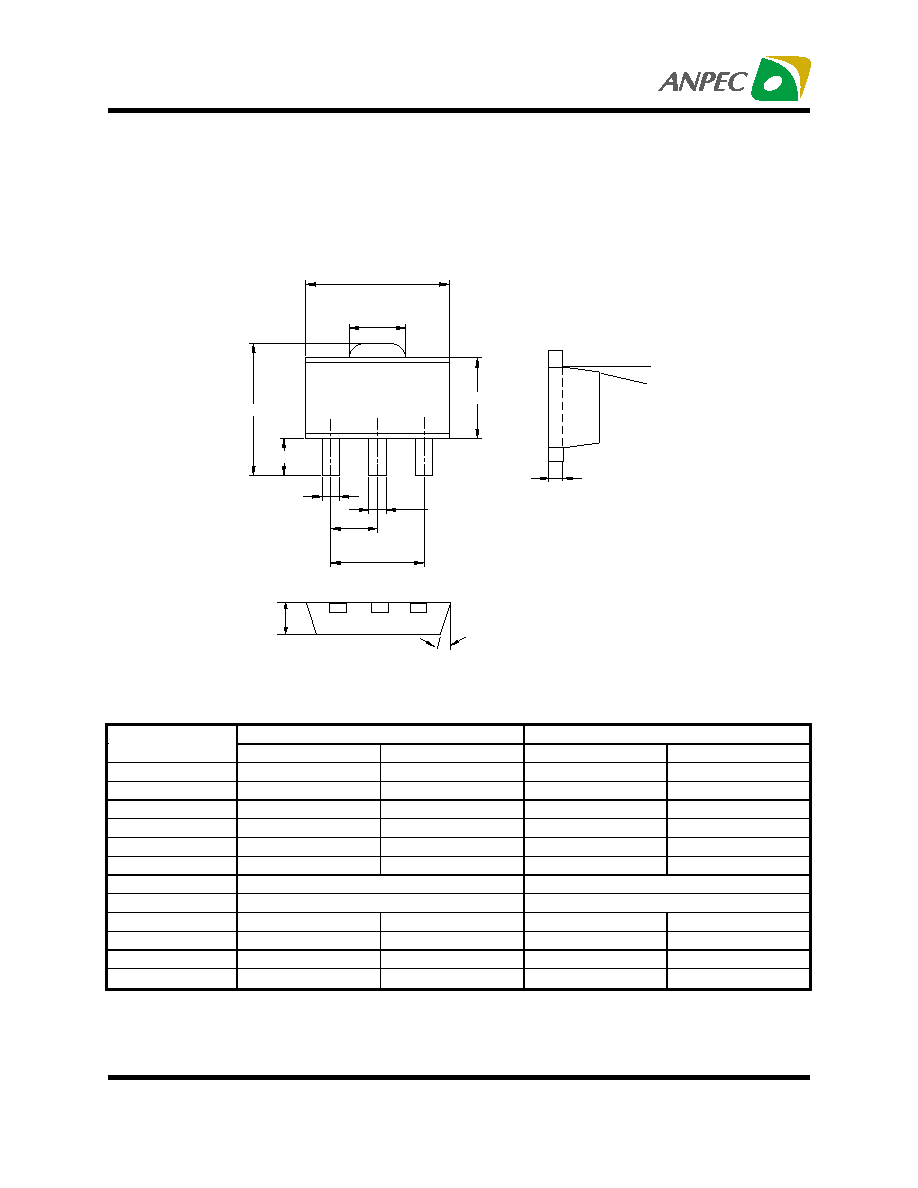
SOT-23
Packaging Information
D
E
H
e
A
A1
L
C
B
3
2
1
M illim e te rs In c h e s
D im
M in . M a x . M in . M a x .
A 1 .0 0
1 .3 0
0 .0 3 9
0 .0 5 1
A 1 0 .0 0
0 .1 0
0 .0 0 0
0 .0 0 4
B 0 .3 5
0 .5 1
0 .0 1 4
0 .0 2 0
C 0 .1 0
0 .2 5
0 .0 0 4
0 .0 1 0
D 2 .7 0
3 .1 0
0 .1 0 6
0 .1 2 2
E 1 .4 0
1 .8 0
0 .0 5 5
0 .0 7 1
e 1 .9 0 /2 .1
B S C
0 .0 7 5 /0 .0 8 3
B S C
H 2 .4 0
3 .0 0
0 .0 9 4
0 .11 8
L 0 .3 7
0 .0 1 5
Copyright
ANPEC Electronics Corp.
Rev. A.6 - Mar., 2004
APL5508/5508R/5509/5509R
www.anpec.com.tw
9
SOT-89 (Reference EIAJ ED-7500A Reg stration SC-62)
Packaging Information
M illim eters
Inches
Dim
M in.
M ax.
M in.
M ax.
A
1.40
1.60
0.055
0.063
B
0.40
0.56
0.016
0.022
B1
0.35
0.48
0.014
0.019
C
0.35
0.44
0.014
0.017
D
4.40
4.60
0.173
0.181
D1
1.35
1.83
0.053
0.072
e
1.50 BSC
0.059 BSC
e1
3.00 BSC
0.118 BSC
E
2.29
2.60
0.090
0.102
H
3.75
4.25
0.148
0.167
L
0.80
1.20
0.031
0.047
10
∞
10
∞
D
D1
e
B1
e1
B
1
2
3
L
H
E
C
a
a
A
Copyright
ANPEC Electronics Corp.
Rev. A.6 - Mar., 2004
APL5508/5508R/5509/5509R
www.anpec.com.tw
10
Package Information
SOT-223( Reference JEDEC Registration SOT-223)
B1
D
H
E
K
e
e1
A
c
L
A1
a
B
b
Millimeters
Inches
Dim
Min.
Max.
Min.
Max.
A
1.50
1.80
0.06
0.07
A1
0.02
0.08
B
0.60
0.80
0.02
0.03
B1
2.90
3.10
0.11
0.12
c
0.28
0.32
0.01
0.01
D
6.30
6.70
0.25
0.26
E
3.30
3.70
0.13
0.15
e
2.3 BSC
0.09 BSC
e1
4.6 BSC
0.18 BSC
H
6.70
7.30
0.26
0.29
L
0.91
1.10
0.04
0.04
K
1.50
2.00
0.06
0.08
0
∞
10
∞
0
∞
10
∞
13
∞
13
∞

Copyright
ANPEC Electronics Corp.
Rev. A.6 - Mar., 2004
APL5508/5508R/5509/5509R
www.anpec.com.tw
11
Terminal Material
Solder-Plated Copper (Solder Material : 90/10 or 63/37 SnPb), 100%Sn
Lead Solderability
Meets EIA Specification RSI86-91, ANSI/J-STD-002 Category 3.
Physical Specifications
Reflow Condition
(IR/Convection or VPR Reflow)
Classification Reflow Profiles
t 25 C to Peak
tp
Ram p-up
t
L
Ram p-down
ts
Preheat
Tsm ax
Tsm in
T
L
T
P
25
Tem
p
e
r
at
ur
e
Tim e
Critical Zone
T
L
to T
P
∞
Profile Feature
Sn-Pb Eutectic Assembly
Pb-Free Assembly
Average ramp-up rate
(T
L
to T
P
)
3
∞
C/second max.
3
∞
C/second max.
Preheat
-
Temperature Min (Tsmin)
-
Temperature Max (Tsmax)
-
Time (min to max) (ts)
100
∞
C
150
∞
C
60-120 seconds
150
∞
C
200
∞
C
60-180 seconds
Time maintained above:
-
Temperature (T
L
)
-
Time (t
L
)
183
∞
C
60-150 seconds
217
∞
C
60-150 seconds
Peak/Classificatioon Temperature (Tp)
See table 1
See table 2
Time within 5
∞
C of actual
Peak Temperature (tp)
10-30 seconds
20-40 seconds
Ramp-down Rate
6
∞
C/second max.
6
∞
C/second max.
Time 25
∞
C to Peak Temperature
6 minutes max.
8 minutes max.
Notes: All temperatures refer to topside of the package .Measured on the body surface.
Copyright
ANPEC Electronics Corp.
Rev. A.6 - Mar., 2004
APL5508/5508R/5509/5509R
www.anpec.com.tw
12
R e lia b ility te s t p ro g ra m
Te s t ite m
M e th o d
D e s c rip tio n
S O L D E R A B IL IT Y
M IL -S T D -8 8 3 D -2 0 0 3
2 4 5
∞
C , 5 S E C
H O LT
M IL -S T D -8 8 3 D -1 0 0 5 .7
1 0 0 0 H rs B ia s @ 1 2 5
∞
C
P C T
J E S D -2 2 -B , A 1 0 2
1 6 8 H rs , 1 0 0 % R H , 1 2 1
∞
C
T S T
M IL -S T D -8 8 3 D -1 0 11 .9
-6 5
∞
C ~ 1 5 0
∞
C , 2 0 0 C y c le s
E S D
M IL -S T D -8 8 3 D -3 0 1 5 .7
V H B M > 2 K V, V M M > 2 0 0 V
L a tc h -U p
J E S D 7 8
1 0 m s , I
tr
> 1 0 0 m A
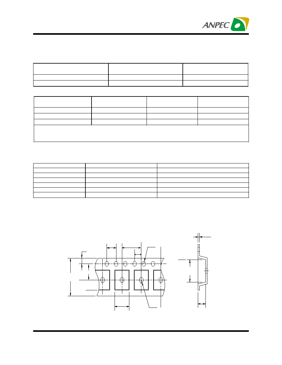
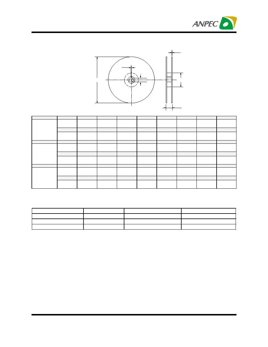
Carrier Tape
t
Ao
E
W
Po
P
Ko
Bo
D1
D
F
P1
Table 1. SnPb Entectic Process ≠ Package Peak Reflow Tem peratures
Package Thickness
Volume mm
3
<350
Volume mm
3
350
<2.5 m m
240 +0/-5
∞
C 225
+0/-5
∞
C
2.5 m m
225 +0/-5
∞
C 225
+0/-5
∞
C
Table 2. Pb-free Process ≠ Package Classification Reflow Tem peratures
Package Thickness
Volume mm
3
<350
Volume mm
3
350-2000
Volume mm
3
>2000
<1.6 m m
260 +0
∞
C* 260
+0
∞
C* 260
+0
∞
C*
1.6 m m ≠ 2.5 m m
260 +0
∞
C* 250
+0
∞
C* 245
+0
∞
C*
2.5 m m
250 +0
∞
C* 245
+0
∞
C* 245
+0
∞
C*
*Tolerance: The device m anufacturer/supplier shall assure process com patibility up to and
including the stated classification tem perature (this m eans Peak reflow tem perature +0
∞
C.
For exam ple 260
∞
C+0
∞
C) at the rated MSL level.
Classification Reflow Profiles(Cont.)
Copyright
ANPEC Electronics Corp.
Rev. A.6 - Mar., 2004
APL5508/5508R/5509/5509R
www.anpec.com.tw
13
A p p lic a tion
A
B
C
J
T 1
T 2
W
P
E
1 78
±
1
6 0
±
1 .0
1 2.0
2 .5
±
0 .15
9 .0
±
0 .5
1 .4
8 .0 + 0.3
- 0.3
4 .0
1 .7 5
F
D
D 1
P o
P 1
A o
B o
K o
t
S O T -23
3 .5
±
0 .05
1 .5 + 0.1
0 .1 M IN
4 .0
2 .0
±
0 .05
3 .1
3 .0
1 .3
0 .2
±
0 .03
A p p lic a tion
A
B
C
J
T 1
T 2
W
P
E
1 78
±
1
7 0
±
2
1 3.5
±
0.15
3
±
0 .1 5
1 4
±
2
1 .3
±
0 .3
1 2 + 0.3
1 2 - 0 .1
8
±
0 .1
1 .7 5
±
0 .1
F
D
D 1
P o
P 1
A o
B o
K o
t
S O T -89
5 .5
±
0 .05
1 .5
±
0 .1
1 .5
±
0 .1
4 .0
±
0 .1
2 .0
±
0 .1
4 .8
±
0 .1
4 .5
±
0 .1
1 .8 0
±
0 .1
0 .3
±
0 .01 3
A p p lic a tion
A
B
C
J
T 1
T 2
W
P
E
3 30
±
1
6 2
±
1 .5
1 2.7 5
±
0 .1 5
2
±
0 .6
1 2.4 + 0.2
2
±
0 .2
1 2
±
0 .3
8
±
0 .1
1 .7 5
±
0 .1
F
D
D 1
P o
P 1
A o
B o
K o
t
S O T -22 3
5 .5
±
0 .05
1 .5 + 0.1
1 .5 + 0.1
4 .0
±
0 .1
2 .0
±
0 .05
6 .9
±
0 .1
7 .5
±
0 .1
2 .1
±
0 .1
0 .3
±
0 .05
Application
Carrier Width
Cover Tape Width
Devices Per Reel
SOT- 23
8
5.3
3000
SOT- 89
12
9.3
1000
SOT- 223
12
9.3
2500
Cover Tape Dimensions
Anpec Electronics Corp.
Head Office :
5F, No. 2 Li-Hsin Road, SBIP,
Hsin-Chu, Taiwan, R.O.C.
Tel : 886-3-5642000
Fax : 886-3-5642050
Taipei Branch :
7F, No. 137, Lane 235, Pac Chiao Rd.,
Hsin Tien City, Taipei Hsien, Taiwan, R. O. C.
Tel : 886-2-89191368
Fax : 886-2-89191369
Customer Service
Carrier Tape(Cont.)
(mm)
A
J
B
T2
T1
C