
Copyright
©
ANPEC Electronics Corp.
Rev. A.1 - Jun., 2006
APW7067N
www.anpec.com.tw
1
ANPEC reserves the right to make changes to improve reliability or manufacturability without notice, and
advise customers to obtain the latest version of relevant information to verify before placing orders.
Synchronous Buck PWM and Linear Controller
Features
∑
Provided Two Regulated Voltages
- Synchronous Buck Converter
- Linear Regulator
∑
Single 12V Power Supply Required
∑
Excellent Both Output Voltage Regulation
- 0.8V Internal Reference
- ±1% Over Line Voltage and Temperature
∑
Integrated Soft-Start for PWM and Linear Outputs
∑
Programmable Frequency Range
from 150 kHz to 1000kHz
∑
Voltage Mode PWM Control Design and
Up to 89% (Typ.) Duty Cycle
∑
Under-Voltage Protection for PWM and Linear
Output
∑
Over-Current Protection for PWM Output
- Sense Low-Side MOSFET's R
DS(ON)
∑
SOP-14, QSOP-16 and QFN-16 packages
∑
Lead Free Available (RoHS Compliant)
Applications
General Description
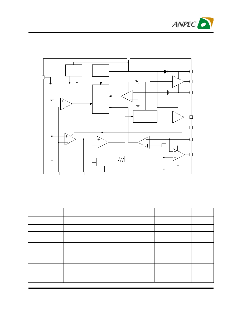
The APW7067N integrates synchronous buck PWM
and linear controller, as well as monitoring and pro-
tection functions into a single package. The synchro-
nous PWM controller drives dual N-channel MOSFETs,
which provides one controlled power output with under-
voltage and over-current protections. Linear controller
drives an external N-channel MOSFET with under-volt-
age protection.
The APW7067N provides excellent regulation for output
load variation. An internal 0.8V temperature-compensated
reference voltage is designed to meet the requirement
of low output voltage applications. The switching
frequency is adjustable from 150kHz to 1000kHz.
The APW7067N with excellent protection functions:
POR, OCP and UVP. The Power-On Reset (POR)
circuit can monitor VCC12 supply voltage exceeds
its threshold voltage while the controller is running,
and a built-in digital soft-start provides both outputs
with controlled rising voltage. The Over-Current Protection
(OCP) monitors the output current by using the voltage
drop across the lower MOSFET's R
DS(ON)
, comparing
with internal V
OCP
(0.25V), eliminating the need for a
current sensing resister. When the output current
reaches the trip point, the controller will shutdown the
IC directly, and latch the converter's output. The
Under-Voltage Protection (UVP) monitors the voltages
of FB and FBL pins for short-circuit protection. When
the V
FB
or V
FBL
is less than 50% of V
REF
, the controller
will shutdown the IC directly.
∑
Graphic Cards
Copyright
©
ANPEC Electronics Corp.
Rev. A.1 - Jun., 2006
APW7067N
www.anpec.com.tw
2
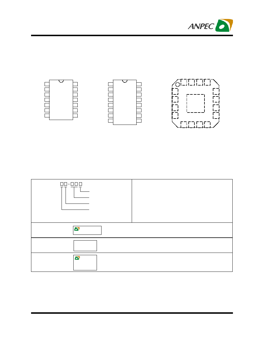
Ordering and Marking Information
Pinouts
APW7067N
Handling Code
Temp. Range
Package Code
Package Code
K : SOP - 14 M : QSOP - 16 QA : QFN - 16
Temp. Range
E : -20 to 70 C
Handling Code
TU : Tube
TR : Tape & Reel
TY : Tray (for QFN only)
Lead Free Code
L : Lead Free Device Blank : Original Device
∞
APW7067N K :
APW7067N
XXXXX
XXXXX - Date Code
Lead Free Code
APW7067N Q :
APW7067N
XXXXX
XXXXX - Date Code
APW7067N M :
APW7067N
XXXXX
XXXXX - Date Code
Note: ANPEC lead-free products contain molding compounds/die attach materials and 100% matte tin plate
termination finish; which are fully compliant with RoHS and compatible with both SnPb and lead-free soldering
operations. ANPEC lead-free products meet or exceed the lead-free requirements of IPC/JEDEC J STD-020C
for MSL classification at lead-free peak reflow temperature.
1
3
2
4
6
5
7
8
BOOT
FS_DIS
DRIVE
FB
COMP
GND
FBL
GND
16
14
15
13
11
12
10
9
UGATE
PHASE
NC
LGATE
PGND
VCC12
NC
VCC12
QSOP-16
TOP VIEW
1
3
2
4
6
5
7
BOOT
FS_DIS
DRIVE
FB
COMP
GND
FBL
14
12
13
11
9
10
8
UGATE
PHASE
NC
LGATE
PGND
VCC12
NC
SOP-14
TOP VIEW
1
3
2
4
6
5
7
8
B
O
O
T
F
S
_
D
I
S
DRIVE
FB
COMP
A
G
N
D
FBL
D
G
N
D
U
G
A
T
E
P
H
A
S
E
NC
LGATE
PGND
V
C
C
1
2
NC
V
C
C
1
2
QFN-16
TOP VIEW
12
10
11
9
15
16
14
13
Metal
GND Pad
(Bottom)
Copyright
©
ANPEC Electronics Corp.
Rev. A.1 - Jun., 2006
APW7067N
www.anpec.com.tw
3
Block Diagram
Symbol
Parameter
Rating
Unit
VCC12
VCC12 to GND
-0.3 to +16
V
BOOT
BOOT to PHASE
-0.3 to +16
V
UGATE
UGATE to PHASE <400ns pulse width
>400ns pulse width
-5 to BOOT+5
-0.3 to BOOT+0.3
V
LGATE
LGATE to PGND <400ns pulse width
>400ns pulse width
-5 to VCC12+5
-0.3 to VCC12+0.3
V
PHASE
PHASE to GND <400ns pulse width
>400ns pulse width
-5 to +21
-0.3 to 16
V
DRIVE
DRIVE to GND
12
V
FB, FBL, COMP,
FS_DIS
FB, FBL, COMP, FS_DIS to GND
-0.3 to 7
V
Absolute Maximum Ratings
Gate Control
Soft Start
and
Fault Logic
Power-On
Reset
PHASE
LGATE
FB
VCC12
UGATE
V
REF
50%V
REF
O.C.P
Comparator
Error
Amp 1
PWM
Comparator
U.V.P
Comparator
:
2
COMP
BOOT
V
REF
50%V
REF
:
2
FBL
DRIVE
Oscillator
FS_DIS
GND
U.V.P
Comparator
V
OCP
0.25V
PGND
Regulator
V
REF
(0.8V)
10V
10V
Error
Amp 2
Sawtooth
wave
Sense Low Side
Copyright
©
ANPEC Electronics Corp.
Rev. A.1 - Jun., 2006
APW7067N
www.anpec.com.tw
4
Symbol
Parameter
Rating
Unit
PGND
PGND to GND
-0.3 to +0.3
V
T
J
Junction Temperature Range
-20 to +150
∞
C
T
STG
Storage Temperature
-65 ~ 150
∞
C
T
SDR
Soldering Temperature (10 Seconds)
300
∞
C
V
ESD
Minimum ESD Rating
±
2
KV
Absolute Maximum Ratings (Cont.)
Symbol
Parameter
Rating
Unit
VCC12
IC Supply Voltage
10.8 to 13.2
V
V
IN1
Converter Input Voltage
2.9 to 13.2
V
V
OUT1
Converter Output Voltage
0.9 to 5
V
I
OUT1
Converter Output Current
0 to 30
A
I
OUT2
Linear Output Current
0 to 3
A
T
A
Ambient Temperature Range
-20 to 70
∞
C
T
J
Junction Temperature Range
-20 to 125
∞
C
Recommended Operating Conditions
Electrical Characteristics
APW7067N
Symbol
Parameter
Test Conditions
Min
Typ
Max
Unit
INPUT SUPPLY CURRENT
VCC12 Supply Current
(Shutdown mode)
UGATE, LGATE and DRIVE open;
FS_DIS = GND
4
6
mA
I
CC12
VCC12 Supply Current
UGATE, LGATE and DRIVE open;
F
OSC
= 600kHz
16
24
mA
POWER-ON RESET
Rising VCC12 Threshold
7.7
7.9
8.1
V
Falling VCC12 Threshold
7.2
7.4
7.6
V
Unless otherwise specified, these specifications apply over VCC12 = 12V, and T
A
=-20 ~ 70
∞
C. Typical values
are at T
A
= 25
∞
C.
NOTE1: Absolute Maximum Ratings are those values beyond which the life of a device may be impaired.
Exposure to absolute maximum rating conditions for extended periods may affect device reliability.
NOTE2: The device is ESD sensitive. Handling precautions are recommended.
Copyright
©
ANPEC Electronics Corp.
Rev. A.1 - Jun., 2006
APW7067N
www.anpec.com.tw
5
Electrical Characteristics (Cont.)
APW7067N
Symbol
Parameter
Test Conditions
Min
Typ
Max
Unit
OSCILLATOR
Accuracy
-15
+15
%
F
OSC
Oscillator Frequency
R
FS_DIS
= 110k ohms
255
300
345
kHz
F
OSC
Oscillator Frequency
R
FS_DIS
= 47k ohms
510
600
690
kHz
V
OSC
Ramp Amplitude
(nominal 1.2V to 2.7V) (NOTE3)
1.5
V
Duty Maximum Duty Cycle
89
%
REFERENCE
V
REF
Reference Voltage
for Error Amp1 and Amp2
0.792 0.80 0.808
V
Reference Voltage Tolerance
-1
+1
%
%
PWM Load Regulation
I
OUT1
= 0 to 10A
1
%
%
Linear Load Regulation
I
OUT2
= 0 to 3A
1
%
%
PWM ERROR AMPLIFIER
Gain Open Loop Gain
R
L
= 10k, C
L
= 10pF (NOTE3)
93
dB
GBWP Open Loop Bandwidth
R
L
= 10k, C
L
= 10pF (NOTE3)
20
MHz
SR
Slew Rate
R
L
= 10k, C
L
= 10pF (NOTE3)
8
V/us
FB Input Current
V
FB
= 0.8V
0.1
1
uA
V
COMP
COMP High Voltage
5
V
V
COMP
COMP Low Voltage
0
V
I
COMP
COMP Source Current
COMP = 2V
12
mA
I
COMP
COMP Sink Current
COMP = 2V
12
mA
GATE DRIVERS
I
UGATE
Upper Gate Source Current
2.5
A
I
UGATE
Upper Gate Sink Current
BOOT = 12V,
UGATE-PHASE = 2V
2
A
I
LGATE
Lower Gate Source Current
2.5
A
I
LGATE
Lower Gate Sink Current
VCC12 = 12V, LGATE = 2V
3.5
A
R
UGATE
Upper Gate Source Impedance BOOT = 12V, I
UGATE
= 0.1A
2.25 3.375
R
UGATE
Upper Gate Sink Impedance
BOOT = 12V, I
UGATE
= 0.1A
0.7
1.05
R
LGATE
Lower Gate Source Impedance VCC12 = 12V, I
LGATE
= 0.1A
2.25 3.375
R
LGATE
Lower Gate Sink Impedance
VCC12 = 12V, I
LGATE
= 0.1A
0.4
0.6
T
D
Dead Time
20
nS
Unless otherwise specified, these specifications apply over VCC12 = 12V, and T
A
=-20 ~ 70
∞
C. Typical values
are at T
A
= 25
∞
C.