Copyright
©
ANPEC Electronics Corp.
Rev. A.2 - Jul., 2005
APX6223
www.anpec.com.tw
1
ANPEC reserves the right to make changes to improve reliability or manufacturability without notice, and advise
customers to obtain the latest version of relevant information to verify before placing orders.
DSC Motors Driver IC
∑
H Bridges Independent Control
∑
Channels Saturation Voltage Drive, One Channel
Constant Voltage Drive and One Channel
Constant Current Drive
∑
Support DSC Exposure/Shutter/Focus/Zoom
Motor Driving
∑
Power Save Mode
∑
Lower Power Excitation Mode for Constant
Current H Bridge
∑
Thermal Shutdown Protection
∑
Low Voltage Detection
∑
Lower Voltage Operation From 2.5V ~ 5.5V
∑
CMOS Process, Lower Power Consumption
∑
Compact Design for Small Size Package
∑
Lead Free Available (RoHS Compliant)
∑
Digital Still Camera for Exposure/Shutter/
Focus/Zoom Motor Driving
The APX6223 CMOS integrated circuit builds driving
capability for Digital Still Camera Exposure/Shutter/
Focus/Zoom motor operation. Independent control
inputs drive Saturation, Constant voltage and Constant
current H bridge.
Advanced CMOS processing is used to take advantage
of low-voltage and low-power requirements. A power
saving mood can optimize the energy saving in portable
application. The APX6223 comes in a miniature 48-pin
LQFP and TQFN packages.
Features
General Description
Applications
APX6223
Package Code
QD : LQFP - 48 QB : TQFN - 48
Operating Ambient Temp. Range
I : -40 to 85 C
Handling Code
TY : Tray
Lead Free Code
L : Lead Free Device Blank : Original Device
∞
Handling Code
Temp. Range
Package Code
XXXXX - Date Code
APX6223 QD/QB :
APX6223
XXXXX
Lead Free Code
Ordering and Marking Information
Note: ANPEC lead-free products contain molding compounds/die attach materials and 100% matte tin plate
termination finish; which are fully compliant with RoHS and compatible with both SnPb and lead-free soldiering
operations. ANPEC lead-free products meet or exceed the lead-free requirements of IPC/JEDEC J STD-020C
for MSL classification at lead-free peak reflow temperature.
Copyright
©
ANPEC Electronics Corp.
Rev. A.2 - Jul., 2005
APX6223
www.anpec.com.tw
2
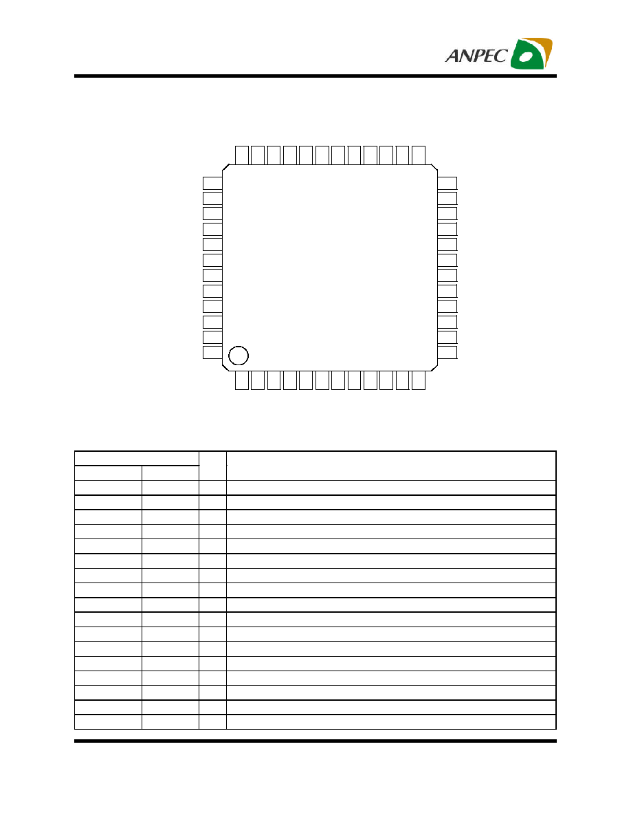
Pin Configuration
Pin Description
37
VC6A
38
DGND
39
PGND34
40
OUT3B
41
VBB34
42
43
44
OUT4B
45
46
47
48
VREFCT
PGND34
OUT3A
VBB34
OUT4A
PGND34
24
BRK
23
VDD
22
PGND12
21
OUT2B
20
VBB12
19
18
17
OUT1B
16
15
14
13
PS
PGND12
OUT2A
VBB12
OUT1A
PGND12
25
VREF
26
VC5
27
OUT5A
28
VBB5
29
OUT5B
30
31
32
OUT6A
33
34
35
36
VC6
VBB6
PGND12
RNF6
OUT6B
VBB6
12
11
10
9
8
7
6
5
4
3
2
1
IN6B
IN6A
IN5B
IN5A
IN4B
IN4A/EN4
IN3B
IN3A/EN3
IN2B
IN2A/EN2
IN1B
IN1A/EN1
APX6223
PIN
No.
Name
I/O
Description
1
IN6B
I Input B of channel 6 H bridge
2
IN6A
I Input A of channel 6 H bridge
3
IN5B
I Input B of channel 5 H bridge
4
IN5A
I Input A of channel 5 H bridge
5
IN4B
I Input B of channel 4 H bridge
6
IN4A/EN4
I Input A of channel 4 H bridge, or enable control
7
IN3B
I Input B of channel 3 H bridge
8
IN3A/EN3
I Input A of channel 3 H bridge, or enable control
9
IN2B
I Input B of channel 2 H bridge
10
IN2A/EN2
I Input A of channel 2 H bridge, or enable control
11
IN1B
I Input B of channel 1 H bridge
12
IN1A/EN1
I Input A of channel 1 H bridge, or enable control
13
PS
I Power save mode, H: circuit operation, L: stand by
14,18,22
PGND12
H bridge channel 1,2 power GND
15
OUT1A
O H bridge channel 1 output A
16,20
VBB12
H bridge channel 1,2 power source
17
OUT1A
O H bridge channel 1 output B
Copyright
©
ANPEC Electronics Corp.
Rev. A.2 - Jul., 2005
APX6223
www.anpec.com.tw
3
Pin Description (Cont.)
PIN
No.
Name
I/O
Description
19
OUT2A
O
H bridge channel 2 output A
21
OUT2B
O
H bridge channel 2 output B
23
V
DD
Power source for control logic
24
BRK
I
Set mode brake function for channel 1~4
25
V
REF
O
1.2 V, this is a input voltage for resistors divider to generate the VC6
voltage
26
VC5
O
The voltage of VOUT5A, VOUT5B is four times large as VC5, output
will be saturated once the VC5=V
DD
27
OUT5A
O H bridge channel 5 output A
28
VBB5
H bridge channel 5 power source
29
OUT5B
O H bridge channel 5 output B
30
PGND5
H bridge channel 5 power GND
31,35
VBB6
H bridge channel 6 power source
32
OUT6A
O H bridge channel 6 output A
33
RNF6
I
Channel 6 motor drive current sense, connect a resistor between
this terminal and GND
34
OUT6B
O H bridge channel 6 output B
36
VC6
I
Channel 6 comparator input
37
VC6A
I
Channel 6 comparator adjustable input
38
GND
Control logic GND
39,43,47
PGND34
H bridge channel 3,4 power GND
40
OUT3B
O H bridge channel 3 output B
41,45
VBB34
H bridge channel 3,4 power source
42
OUT3A
O H bridge channel 3 output A
44
OUT4B
O H bridge channel 4 output B
46
OUT4A
O H bridge channel 4 output A
48
V
REFCT
I
Motor excitation saving control, set H save control, set L normal
control, only valid for channel 6 current driving
Copyright
©
ANPEC Electronics Corp.
Rev. A.2 - Jul., 2005
APX6223
www.anpec.com.tw
4
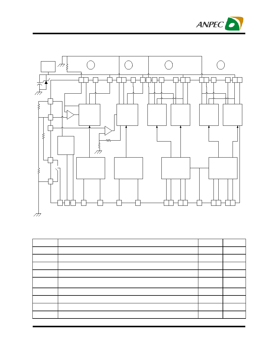
Block Diagram
Logic
Control
Logic
Control
Logic
Control
Logic
Control
Constant current
H
Birdge
(6CH)
Constant Voltage
H
Bridge
(5CH)
Saturation drive
H
Bridge
(4CH)
Saturation drive
H
Bridge
(3CH)
Saturation drive
H
Bridge
(2CH)
Saturation drive
H
Bridge
(1CH)
DC
Zoom
Stepping
Focus
VCM
Shutter
TSD
Bias circuit
Low Voltage
Protection
Power save
33
44
12
11
10
9
8
7
6
5
4
3
2
1
13
PS
IN6B
IN6A
IN5A
IN5B
EN3/IN3A
IN3B
EN4/IN4A
IN4B
EN2/IN2A
IN1B
EN1/IN1A
IN2B
24
BRK
34
32
31
35
28
27
29
30
39
43
47
42
41
45
40
46
14
18
22
21
19
17
16
20
15
OUT1A
OUT1B
VBB12
OUT2A
OUT2B
PGND12
OUT3A
OUT3B
VBB34
VBB5
PGND34
OUT4A
OUT4B
OUT5A
OUT5B
PGND12
VBB6
OUT6A
OUT6B
RNF6
23
36
26
VC5
VC6
25
VREF
VDD
48
VREFCT
37
38
VC6A
DGND
VBB
Motor
power
supply
Stepping
or DC
Iris
M
M
M
M
Absolute Maximum Ratings
Symbol
Parameter
Rating
Unit
V
DD
Logic Supply Voltage
6.5
V
V
BB
Motor Supply Voltage
6.5
V
I
O
Peak Output Current (1ch ~ 6ch)
+-800
mA
I
O
Continuous Output Current (1ch ~ 6ch)
+-500
mA
R
T JA
Thermal Resistance ≠ Junction to Ambient
LQFP 48
125
∞
C/W
T
J
Junction Temperature
0 to 150
∞
C
T
OP
Operating Temperature Range
0 to 70
∞
C
T
STG
Storage Temperature Range
-65 to +150
∞
C
T
L
Lead Temperature (Soldering, 10 second)
260
∞
C
Copyright
©
ANPEC Electronics Corp.
Rev. A.2 - Jul., 2005
APX6223
www.anpec.com.tw
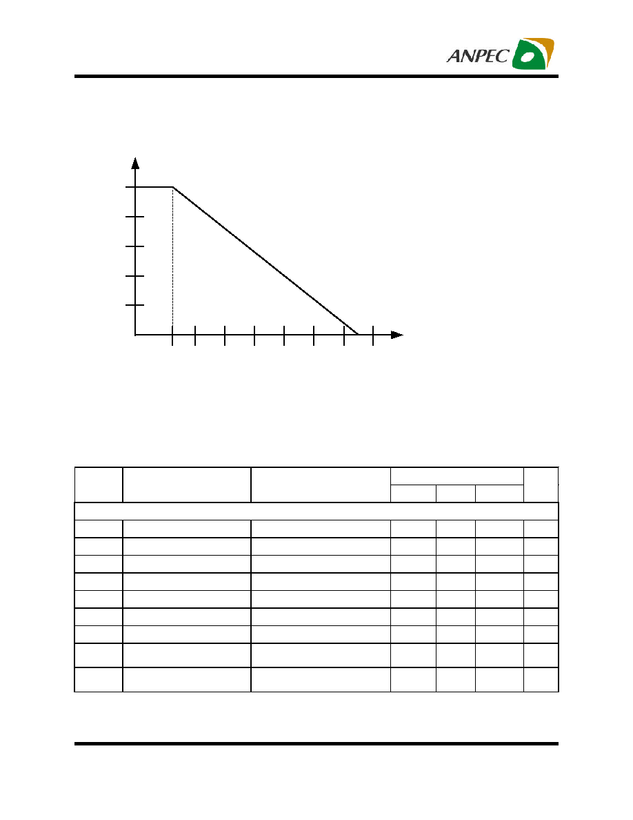
5
1000
800
600
400
200
0
25
40
60
80
100 120
140
160
Power dissipation(mW)
Ambient temperature ,T
A
(
)
C
∞
Electrical Characteristics
Unless otherwise noted these specifications apply over full temperature, V
BB
= 5V, V
DD
= 3V,
T
A
= -40 to 85
∞
C. Typical values refer to T
A
=
25
∞
C.
APX6223
Symbol
Parameter
Condition
Min.
Typ.
Max.
Unit
Control logic
V
IH
High Input Voltage
All inputs
V
DD
x 0.7
V
V
IL
Low Input Voltage
All inputs
V
DD
x 0.3
V
I
IH
High Input Current
V
IN
= V
DD
= 3V
15
30
60
µ
A
I
IL
Low Input Current
-1
µ
A
V
REF
Reference Voltage
1.13
1.21
1.29
V
I
DD
(on) Supply Current
V
DD
= 3V, V
BB
= 5V, PS = H
1.0
2.0
mA
I
DD
(stb) Standby Supply Current
V
DD
= 3V, V
BB
= 5V, PS = L
0.1
5
µ
A
I
BB1
Motor Supply Current
V
DD
= 3V, V
BB
= 5V, PS = L,
sum of V
BB
0.1
5
µ
A
I
BB2
Motor Supply Current
V
DD
= 0V, V
BB
= 5V, PS = L,
sum of V
BB
0.1
5
µ
A
Thermal Characteristics