 | –≠–ª–µ–∫—Ç—Ä–æ–Ω–Ω—ã–π –∫–æ–º–ø–æ–Ω–µ–Ω—Ç: AOL1400L | –°–∫–∞—á–∞—Ç—å:  PDF PDF  ZIP ZIP |

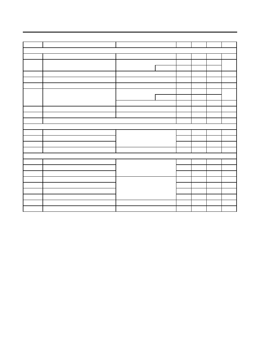
Symbol
V
DS
V
GS
I
DM
I
AR
E
AR
T
J
, T
STG
Symbol
Typ
Max
21
25
48
60
R
JC
1
1.5
∞C
mJ
W
50
W
Repetitive avalanche energy L=0.3mH
C
145
Power Dissipation
A
I
D
Avalanche Current
C
30
T
A
=25∞C
P
DSM
2.1
Power Dissipation
B
Continuous Drain
Current
G
T
A
=25∞C
I
DSM
17
T
A
=70∞C
13
85
70
A
200
A
100
T
C
=100∞C
Continuous Drain
Current
B
Maximum
Units
Parameter
T
C
=25∞C
G
T
C
=100∞C
B
30
∞C/W
Absolute Maximum Ratings T
A
=25∞C unless otherwise noted
V
V
±12
Pulsed Drain Current
Gate-Source Voltage
Drain-Source Voltage
T
C
=25∞C
P
D
Maximum Junction-to-Case
C
Steady-State
T
A
=70∞C
1.3
Junction and Storage Temperature Range
-55 to 175
∞C/W
Thermal Characteristics
Parameter
Units
Maximum Junction-to-Ambient
A
t 10s
R
JA
∞C/W
Maximum Junction-to-Ambient
A
Steady-State
AOL1400
N-Channel Enhancement Mode Field Effect Transistor
Features
V
DS
(V) = 30V
I
D
= 85A (V
GS
= 10V)
R
DS(ON)
< 4.5m
(V
GS
= 10V)
R
DS(ON)
< 5.5m
(V
GS
= 4.5V)
General Description
The AOL1400 uses advanced trench technology to
provide excellent R
DS(ON)
, shoot-through immunity and
good body diode characteristics. This device is ideally
suited for use as a low side switch in CPU core power
conversion.
Standard product AOL1400 is Pb-free
(meets ROHS & Sony 259 specifications). AOL1400L
is a Green Product ordering option. AOL1400 and
AOL1400L are electrically identical.
G
D
S
Ultra
SO-8
TM
Top View
Bottom tab
connected to
drain
Fits SOIC8
footprint !
S
G
D
Alpha & Omega Semiconductor, Ltd.
AOL1400
Symbol
Min
Typ
Max
Units
BV
DSS
30
V
0.005
1
T
J
=55∞C
5
I
GSS
100
nA
V
GS(th)
0.6
1.1
1.8
V
I
D(ON)
100
A
3.9
4.5
T
J
=125∞C
5
6
4.6
5.5
m
g
FS
102
S
V
SD
0.64
1
V
I
S
85
A
C
iss
9130
10500
pF
C
oss
625
pF
C
rss
387
pF
R
g
0.4
0.8
Q
g
(4.5V)
72.4
85
nC
Q
gs
13.4
nC
Q
gd
16.8
nC
t
D(on)
14.7
22
ns
t
r
14.2
21
ns
t
D(off)
105.5
150
ns
t
f
23.5
35
ns
t
rr
30.5
40
ns
Q
rr
21
33
nC
62
THIS PRODUCT HAS BEEN DESIGNED AND QUALIFIED FOR THE CONSUMER MARKET. APPLICATIONS OR USES AS CRITICAL
COMPONENTS IN LIFE SUPPORT DEVICES OR SYSTEMS ARE NOT AUTHORIZED. AOS DOES NOT ASSUME ANY LIABILITY ARISING
OUT OF SUCH APPLICATIONS OR USES OF ITS PRODUCTS. AOS RESERVES THE RIGHT TO IMPROVE PRODUCT DESIGN,
FUNCTIONS AND RELIABILITY WITHOUT NOTICE
Body Diode Reverse Recovery Time
Body Diode Reverse Recovery Charge I
F
=20A, dI/dt=100A/
s
Drain-Source Breakdown Voltage
On state drain current
I
D
=250
A, V
GS
=0V
V
GS
=4.5V, V
DS
=5V
V
GS
=10V, I
D
=20A
Reverse Transfer Capacitance
I
F
=20A, dI/dt=100A/
s
Electrical Characteristics (T
J
=25∞C unless otherwise noted)
STATIC PARAMETERS
Parameter
Conditions
I
DSS
A
Gate Threshold Voltage
V
DS
=V
GS
I
D
=250
A
V
DS
=24V, V
GS
=0V
V
DS
=0V, V
GS
= ±12V
Zero Gate Voltage Drain Current
Gate-Body leakage current
R
DS(ON)
Static Drain-Source On-Resistance
Forward Transconductance
Diode Forward Voltage
Maximum Body-Diode Continuous Current
Input Capacitance
Output Capacitance
DYNAMIC PARAMETERS
m
V
GS
=4.5V, I
D
=20A
I
S
=1A,V
GS
=0V
V
DS
=5V, I
D
=20A
Turn-On Rise Time
Turn-Off DelayTime
V
GS
=10V, V
DS
=15V, R
L
=0.75
,
R
GEN
=3
Turn-Off Fall Time
Turn-On DelayTime
Gate Drain Charge
V
GS
=0V, V
DS
=15V, f=1MHz
SWITCHING PARAMETERS
Total Gate Charge
Gate Source Charge
Gate resistance
V
GS
=0V, V
DS
=0V, f=1MHz
V
GS
=4.5V, V
DS
=15V, I
D
=20A
A: The value of R
JA
is measured with the device mounted on 1in
2
FR-4 board with 2oz. Copper, in a still air environment with T
A
=25∞C. The Power
dissipation P
DSM
is based on R
JA
and the maximum allowed junction temperature of 150∞C. The value in any given application depends on the user's
specific board design, and the maximum temperature of 175∞C may be used if the PCB allows it.
B. The power dissipation P
D
is based on T
J(MAX)
=175∞C, using junction-to-case thermal resistance, and is more useful in setting the upper dissipation
limit for cases where additional heatsinking is used.
C: Repetitive rating, pulse width limited by junction temperature T
J(MAX)
=175∞C.
D. The R
JA
is the sum of the thermal impedence from junction to case R
JC
and case to ambient.
E. The static characteristics in Figures 1 to 6 are obtained using <300
s pulses, duty cycle 0.5% max.
F. These curves are based on the junction-to-case thermal impedence which is measured with the device mounted to a large heatsink, assuming a
maximum junction temperature of T
J(MAX)
=175∞C.
G. The maximum current rating is limited by bond-wires.
H. These tests are performed with the device mounted on 1 in 2 FR-4 board with 2oz. Copper, in a still air environment with T
A
=25∞C.
Rev 1: Dec 2005
Alpha & Omega Semiconductor, Ltd.
AOL1400
TYPICAL ELECTRICAL AND THERMAL CHARACTERISTICS
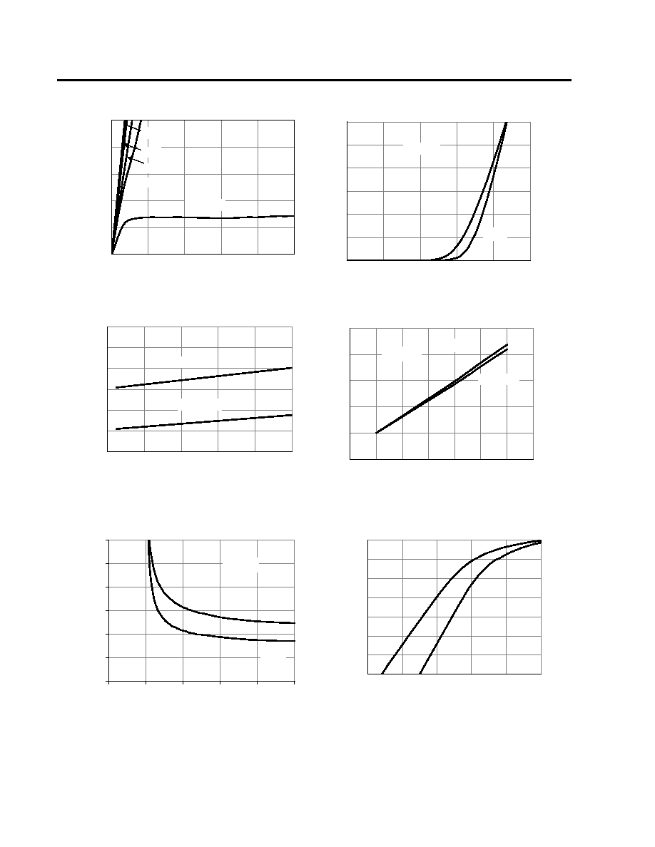
0
20
40
60
80
100
0
1
2
3
4
5
V
DS
(Volts)
Figure 1: On-Region Characteristics
I
D
(A
)
V
GS
=2V
2.5V
10V
3.0V
4.5V
0
10
20
30
40
50
60
0
0.5
1
1.5
2
2.5
V
GS
(Volts)
Figure 2: Transfer Characteristics
I
D
(A
)
3.0
3.5
4.0
4.5
5.0
5.5
6.0
0
20
40
60
80
100
I
D
(A)
Figure 3: On-Resistance vs. Drain Current and
Gate Voltage
R
DS
(
O
N)
(m
)
1.0E-05
1.0E-04
1.0E-03
1.0E-02
1.0E-01
1.0E+00
1.0E+01
1.0E+02
0.0
0.2
0.4
0.6
0.8
1.0
V
SD
(Volts)
Figure 6: Body-Diode Characteristics
I
S
(A
)
25∞C
125∞C
0.8
1
1.2
1.4
1.6
1.8
0
25
50
75
100
125
150
175
Temperature (∞C)
Figure 4: On-Resistance vs. Junction
Temperature
N
o
r
m
a
liz
ed
On
-R
esistan
ce
V
GS
=10V
V
GS
=4.5
0
2
4
6
8
10
12
0
2
4
6
8
10
V
GS
(Volts)
Figure 5: On-Resistance vs. Gate-Source Voltage
R
DS
(
O
N)
(m
)
25∞C
125∞C
V
DS
=5V
V
GS
=4.5V
V
GS
=10V
I
D
=20A
25∞C
125∞C
I
D
=20A
Alpha & Omega Semiconductor, Ltd.
AOL1400
TYPICAL ELECTRICAL AND THERMAL CHARACTERISTICS
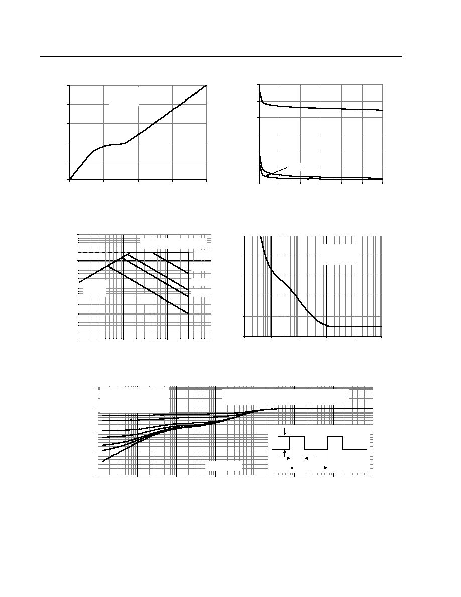
0
1
2
3
4
5
0
20
40
60
80
Q
g
(nC)
Figure 7: Gate-Charge Characteristics
V
GS
(V
ol
ts)
0
2000
4000
6000
8000
10000
12000
0
5
10
15
20
25
30
V
DS
(Volts)
Figure 8: Capacitance Characteristics
C
a
p
acitan
ce (p
F
)
C
iss
0.001
0.01
0.1
1
10
0.00001
0.0001
0.001
0.01
0.1
1
10
100
Pulse Width (s)
Figure 11: Normalized Maximum Transient Thermal Impedance (Note F)
Z
JC
N
o
r
m
a
liz
ed
T
r
an
sien
t
T
h
e
r
m
a
l R
esistan
ce
C
oss
C
rss
V
DS
=15V
I
D
=20A
Single Pulse
D=T
on
/T
T
J,PK
=T
A
+P
DM
.Z
JA
.R
JA
R
JC
=1.5∞C/W
T
on
T
P
D
In descending order
D=0.5, 0.3, 0.1, 0.05, 0.02, 0.01, single pulse
T
J(Max)
=150∞C
T
A
=25∞C
0
200
400
600
800
1000
0.0001
0.001
0.01
0.1
1
10
Pulse Width (s)
Figure 10: Single Pulse Power Rating Junction-to-
Case (Note B)
Po
w
e
r
(
W
)
T
J(Max)
=175∞C
T
A
=25∞C
0.1
1
10
100
1000
0.1
1
10
100
V
DS
(Volts)
I
D
(Am
p
s
)
Figure 9: Maximum Forward Biased Safe
Operating Area (Note F)
10
s
100
s
10ms
1ms
DC
R
DS(ON)
limited
T
J(Max)
=175∞C, T
A
=25∞C
Alpha & Omega Semiconductor, Ltd.
AOL1400
TYPICAL ELECTRICAL AND THERMAL CHARACTERISTICS
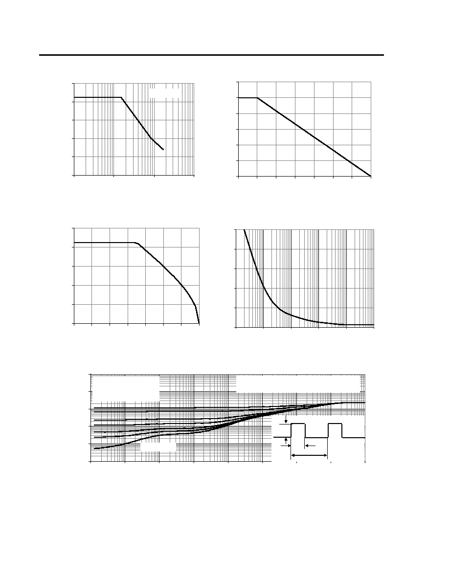
0
20
40
60
80
100
0.00001
0.0001
0.001
0.01
Time in avalanche, t
A
(s)
Figure 12: Single Pulse Avalanche capability
I
D
(A
), P
e
ak A
valan
ch
e C
u
r
r
e
n
t
0
20
40
60
80
100
120
0
25
50
75
100
125
150
175
T
CASE
(∞C)
Figure 13: Power De-rating (Note B)
P
o
w
e
r
D
i
s
s
i
pa
ti
on (W
)
T
A
=25∞C
0
20
40
60
80
100
0
25
50
75
100
125
150
175
T
CASE
(∞C)
Figure 14: Current De-rating (Note B)
C
u
rre
n
t
ra
t
i
n
g
I
D
(A
)
0
20
40
60
80
100
0.01
0.1
1
10
100
1000
Pulse Width (s)
Figure 15: Single Pulse Power Rating Junction-to-
Ambient (Note H)
Po
w
e
r (
W
)
0.001
0.01
0.1
1
10
100
0.00001
0.0001
0.001
0.01
0.1
1
10
100
1000
Pulse Width (s)
Figure 16: Normalized Maximum Transient Thermal Impedance (Note H)
Z
JA
N
o
r
m
a
liz
ed
T
r
an
sien
t
T
h
e
r
m
a
l R
esistan
ce
D=T
on
/T
T
J,PK
=T
A
+P
DM
.Z
JA
.R
JA
R
JA
=60∞C/W
In descending order
D=0.5, 0.3, 0.1, 0.05, 0.02, 0.01, single pulse
T
on
T
P
D
Single Pulse
Alpha & Omega Semiconductor, Ltd.