 | –≠–ª–µ–∫—Ç—Ä–æ–Ω–Ω—ã–π –∫–æ–º–ø–æ–Ω–µ–Ω—Ç: P03A | –°–∫–∞—á–∞—Ç—å:  PDF PDF  ZIP ZIP |
APEX MICROTECHNOLOGY CORPORATION ∑ TELEPHONE (520) 690-8600 ∑ FAX (520) 888-3329 ∑ ORDERS (520) 690-8601 ∑ EMAIL prodlit@apexmicrotech.com
1
FEATURES
∑ MO-127 COPPER POWER DIPTM PACKAGE
∑ HIGH INTERNAL POWER DISSIPATION
-- 500 watts
∑ HIGH VOLTAGE OPERATION -- ±75V
∑ VERY HIGH CURRENT -- ±30 amps
∑ INTERNAL SOA PROTECTION
∑ OUTPUT SWINGS CLOSE TO SUPPLY RAILS
∑ EXTERNAL SHUTDOWN CONTROL
APPLICATIONS
∑ LINEAR AND ROTARY MOTOR DRIVES
∑ YOKE/MAGNETIC FIELD DEFLECTION
∑ PROGRAMMABLE POWER SUPPLIES to ±68V
∑ TRANSDUCER/AUDIO TO 1000W
DESCRIPTION
The super power PA03 advances the state of the art in
both brute force power and self protection against abnormal
operating conditions. Its features start with a copper dip pack-
age developed by Apex to extend power capabilities well
beyond those attainable with the familiar TO-3 package. The
increased pin count of the new package provides additional
control features, while the superior thermal conductivity of
copper allows substantially higher power ratings.
The PA03 incorporates innovative current limiting circuits
limiting internal power dissipation to a curve approximating
the safe operating area of the power transistors. The internal
current limit of 35A is supplemented with thermal sensing
which reduces the current limit as the substrate temperature
rises. Furthermore, a subcircuit monitors actual junction
temperatures and with a response time of less than ten mil-
liseconds reduces the current limit further to keep the junction
temperature at 175∞C.
The PA03 also features a laser trimmed high performance
FET input stage providing superior DC accuracies both initially
and over the full temperature range.
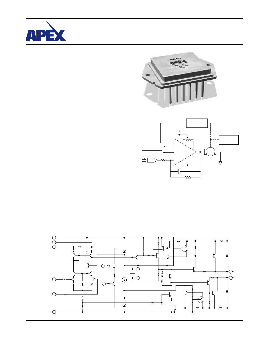
EQUIVALENT
SCHEMATIC
The PA03 output power stages contain fast reverse recovery
diodes for sustained high energy flyback protection.
This hybrid integrated circuit utilizes thick film resistors,
ceramic capacitors and silicon semiconductors to maximize
reliability, minimize size and give top performance. Ultra-
sonically bonded aluminum wires provide reliable intercon-
nections at all operating temperatures. The MO-127 Copper,
12-pin Power DipTM package (see Package Outlines), is
hermetically sealed and isolated from the internal circuits.
Insulating washers are not recommended.
IMPORTANT: Observe mounting precautions.
TYPICAL APPLICATION
12-PIN DIP
PACKAGE STYLE CU
APEX MICROTECHNOLOGY CORPORATION ∑ 5980 NORTH SHANNON ROAD ∑ TUCSON, ARIZONA 85741 ∑ USA ∑ APPLICATIONS HOTLINE: 1 (800) 546-2739
2
ABSOLUTE MAXIMUM RATINGS
SPECIFICATIONS
PA03 ∑ PA03A
ABSOLUTE MAXIMUM RATINGS
PA03
PA03A
PARAMETER
TEST CONDITIONS
2
MIN
TYP
MAX
MIN
TYP
MAX
UNITS
INPUT
OFFSET VOLTAGE, initial
T
C
= 25∞C
± .5
± 2
± .25
± .5
mV
OFFSET VOLTAGE, vs. temperature
Full temperature range
10
30
5
10
µV/∞C
OFFSET VOLTAGE, vs. supply
T
C
= 25∞C
8
*
µV/V
OFFSET VOLTAGE, vs. power
Full temperature range
20
10
µV/W
BIAS CURRENT, initial
T
C
= 25∞C
5
50
3
10
pA
BIAS CURRENT, vs. supply
T
C
= 25∞C
.01
*
pA/V
OFFSET CURRENT, initial
T
C
= 25∞C
2.5
50
1.5
10
pA
INPUT IMPEDANCE, DC
T
C
= 25∞C
10
11
*
INPUT CAPACITANCE
T
C
= 25∞C
6
*
pF
COMMON MODE VOLTAGE RANGE
3
Full temperature range
± V
S
≠10V
*
V
COMMON MODE REJECTION, DC
Full temp. range, V
CM
= ±20V
86
108
*
*
dB
SHUTDOWN CURRENT
4
Full temperature range
100
*
µA
SHUTDOWN VOLTAGE
Full temp. range, amp enabled
.85
*
V
SHUTDOWN VOLTAGE
Full temp. range, amp disabled
3.5
*
V
GAIN
OPEN LOOP GAIN at 10Hz
Full temp. range, full load
92
102
*
*
dB
GAIN BANDWIDTH PRODUCT at 1MHz T
C
= 25∞C, full load
1
*
MHz
POWER BANDWIDTH
T
C
= 25∞C, I
O
= 15A, V
O
= 88V
PP
30
*
kHz
PHASE MARGIN
Full temp. range, C
C
= 1.8nF
65
*
∞
OUTPUT
VOLTAGE SWING
3
T
C
= 25∞C, I
O
= 30A
± V
S
≠7
6.2
*
*
V
VOLTAGE SWING
3
Full temp. range, I
O
= 12A
± V
S
≠5
4.2
*
*
V
VOLTAGE SWING
3
Full temp. range, I
O
= 146mA
± V
S
≠4
3.5
*
*
V
CURRENT, peak
T
C
= 25∞C
30
*
A
SETTLING TIME to .1%
T
C
= 25∞C, 10V step
8
*
µs
SLEW RATE
T
C
= 25∞C, C
C
- open
8
*
V/µs
CAPACITIVE LOAD
Full temp. range, A
V
= 1
2
*
nF
SHUTDOWN DELAY
T
C
= ≠25∞C, disable
10
*
µs
T
C
= ≠25∞C, operate
20
*
µs
POWER SUPPLY
VOLTAGE
Full temperature range
± 15
± 50
± 75
*
*
*
V
CURRENT, quiescent
6
T
C
= 25∞C
125
300
*
*
mA
CURRENT, disable mode
Full temperature range
25
40
*
*
mA
THERMAL
RESISTANCE, AC junction to case
5
Full temp. range, F>60Hz
.22
.28
*
*
∞C/W
RESISTANCE, DC junction to case
Full temp. range, F<60Hz
.25
.3
*
*
∞C/W
RESISTANCE, junction to ambient
Full temperature range
14
*
∞C/W
TEMPERATURE, junction
Sustained operation
150
*
∞C
TEMPERATURE RANGE, case
Meets full range specification
≠ 25
85
*
*
∞C
SPECIFICATIONS
SUPPLY VOLTAGE, +V
S
to ≠V
S
150V
OUTPUT CURRENT, within SOA
Internally limited
POWER DISSIPATION, internal
500W
INPUT VOLTAGE, differential
±25V
INPUT VOLTAGE, common mode
±V
S
TEMPERATURE, pin solder-10s
300∞C
TEMPERATURE, junction
1
175∞C
TEMPERATURE RANGE, storage
≠65 to +150∞C
OPERATING TEMP. RANGE, case
≠55 to +125∞C
SHUTDOWN VOLTAGE, differential
±5V
SHUTDOWN VOLTAGE, common mode
±V
S
NOTES: * The specification of PA03A is identical to the specification for PA03 in applicable column to the left.
1. Long term operation at the maximum junction temperature will result in reduced product life. Derate power dissipation to achieve
high MTTF.
2. The power supply voltage for all specifications is the TYP rating unless noted as a test condition.
3. +V
S
and ≠V
S
denote the positive and negative supply rail respectively. Total V
S
is measured from +V
S
to ≠V
S
.
4. Rating applies if both shutdown inputs are least 1V inside supply rails. If one of the shutdown inputs is tied to a supply rail, the
current in that pin may increase to 2.4mA.
5. Rating applies if the output current alternates between both output transistors at a rate faster than 60Hz.
6. The PA03 must be used with a heatsink or the quiescent power may drive the unit into thermal shutdown.
APEX MICROTECHNOLOGY CORPORATION ∑ TELEPHONE (520) 690-8600 ∑ FAX (520) 888-3329 ∑ ORDERS (520) 690-8601 ∑ EMAIL prodlit@apexmicrotech.com
3
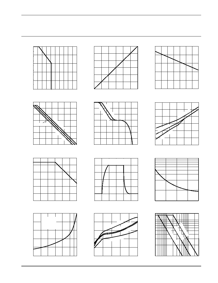
TYPICAL PERFORMANCE
GRAPHS
PA03 ∑ PA03A
APEX MICROTECHNOLOGY CORPORATION ∑ 5980 NORTH SHANNON ROAD ∑ TUCSON, ARIZONA 85741 ∑ USA ∑ APPLICATIONS HOTLINE: 1 (800) 546-2739
4
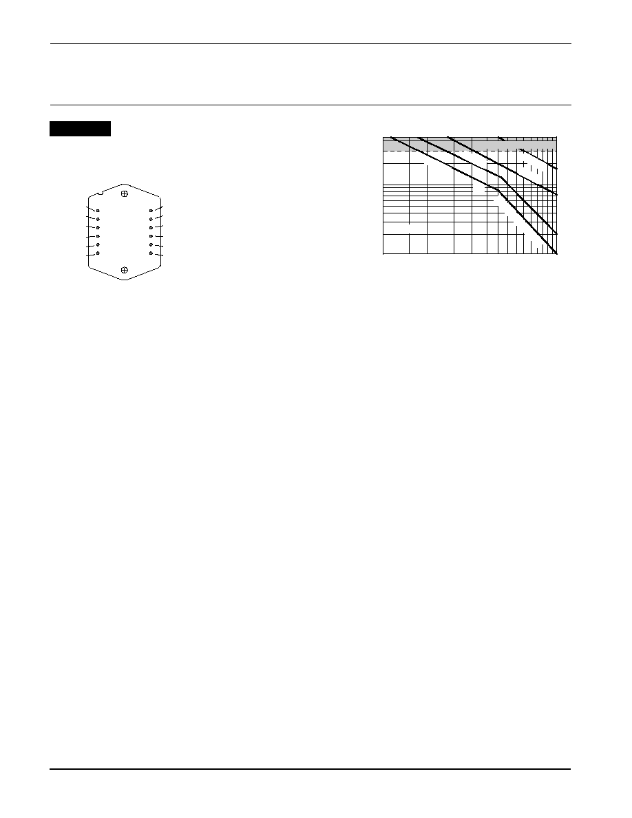
OPERATING
CONSIDERATIONS
PA03 ∑ PA03A
GENERAL
Please read Application Note 1 "General Operating Con-
siderations" which covers stability, supplies, heat sinking,
mounting, current limit, SOA interpretation, and specification
interpretation. Visit www.apexmicrotech.com for design tools
that help automate tasks such as calculations for stability,
internal power dissipation, current limit; heat sink selection;
Apex's complete Application Notes library; Technical Seminar
Workbook; and Evaluation Kits.
MOUNTING PRECAUTIONS
The PA03 copper base is very soft and easily bent. Do not
put any stress on the mounting ears of this package. This calls
for caution when pushing the amplifier into certain types of
packaging foam and particularly when inserting the device into
a socket. Insert the amplifier into the socket only by pushing
on the perimeter of the package lid. Pushing the unit into the
socket by applying pressure to the mounting tabs will bend
the base due to the high insertion force required. The base
will then not contact the heatsink evenly resulting in very poor
heat transfer. To remove a unit from a socket, pry the socket
away from the heatsink so that the heatsink will support the
amplifier base evenly. Recommended mounting torque is 8≠10
in.-lbs. (.9≠1.13 N∑m).
SAFE OPERATING AREA (SOA)
Due to the internal (non-adjustable) current limit of the PA03,
worst case power dissipation calculations must assume cur-
rent capability of 46 amps. Application specific circuits should
be checked against the SOA curve when relying upon current
limit for fault protection.
SAFE OPERATING AREA CURVES
Second breakdown limitations do apply to the PA03 but are
less severe, since junction temperature limiting responds within
10ms. Stress levels shown as being safe for more than 10ms
duration will merely cause thermal shutdown.
Under normal operating conditions, activation of the thermal
shutdown is a sign that the internal junction temperatures have
reached approximately 175∞C. Thermal shutdown is a short
term safety feature. If the conditions remain that cause thermal
shutdown, the amplifier will oscillate in and out of shutdown,
creating peak high power stresses, destroying useful signals,
and reducing the reliability of the device.
BALANCE CONTROL
The voltage offset of the PA03 may be externally adjusted
to zero. To implement this adjustment install a 100 to 200 ohm
potentiometer between pins 11 and 12 and connect the wiper
arm to the positive supply. Bypass pins 11 and 12 each with
at least a .01µF ceramic capacitor.
If the optional adjust provision is not used, connect both
pins 11 and 12 to the positive supply.
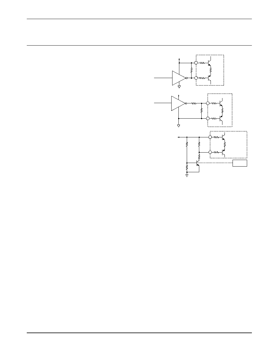
OUTPUT STAGE SHUTDOWN
The entire power stage of the PA03 may be disabled us-
ing one of the circuits shown in Figure 1. There are many
applications for this function. One is a load protection based
on power delivered to the load or thermal rise. Another one is
conservation of power when using batteries. The control voltage
requirements accommodate a wide variety logic drivers.
1. CMOS operating at +5V can drive the control pins di-
rectly.
2. CMOS operating at greater than 5V supplies need a voltage
divider.
3. TTL logic needs a pull up resistor to +5V to provide a swing
to the fully disabled voltage (3.5V). When not using the
shutdown feature, connect both pins 3 and 4 to common.
PHASE COMPENSATION
At low gain settings an external compensation capacitor is
required to insure stability. In addition to the resistive feed-
back network, roll off or integrating capacitors must also be
considered. A frequency of 1 MHz is most appropriate to cal-
culate gain. Operation at gains below 10, without the external
compensation capacitor opens the possibility of oscillations
near output saturation regions when under load, the improper
operation of the thermal shutdown circuit. This can result in
amplifier destruction.
At gains of 10 or more:
1. No external components are required.
2. Typical slew rate will be 8V/µs.
3. Typical phase margin will be 70∞.
EXTERNAL CONNECTIONS
The internal substrate contains beryllia (BeO).
Do not break the seal. If accidentally broken, do
not crush, machine, or subject to temperatures
in excess of 850∞C to avoid generating toxic
fumes.
CAUTION
APEX MICROTECHNOLOGY CORPORATION ∑ TELEPHONE (520) 690-8600 ∑ FAX (520) 888-3329 ∑ ORDERS (520) 690-8601 ∑ EMAIL prodlit@apexmicrotech.com
5
This data sheet has been carefully checked and is believed to be reliable, however, no responsibility is assumed for possible inaccuracies or omissions. All specifications are subject to change without notice.
PA03U REV. I FEBRUARY 1998 © 1998 Apex Microtechnology Corp.
OPERATING
CONSIDERATIONS
PA03 ∑ PA03A
At a gain of 3:
1. Connect a 470pF compensation capacitor between pins 9
and 10.
2. Typical slew rate will be 5V/µs.
3. Typical phase margin will be 45∞.
At unity gain:
1. Connect a 1.8nF compensation capacitor between pins 9
and 10.
2. Typical slew rate will be 1.8V/µs.
3. Typical phase margin will be 65∞.