 | –≠–ª–µ–∫—Ç—Ä–æ–Ω–Ω—ã–π –∫–æ–º–ø–æ–Ω–µ–Ω—Ç: PA240 | –°–∫–∞—á–∞—Ç—å:  PDF PDF  ZIP ZIP |

APEX MICROTECHNOLOGY CORPORATION ∑ TELEPHONE (520) 690-8600 ∑ FAX (520) 888-3329 ∑ ORDERS (520) 690-8601 ∑ EMAIL prodlit@apexmicrotech.com
1
FEATURES
∑ RoHS COMPLIANT
∑ MONOLITHIC MOS TECHNOLOGY
∑ LOW COST
∑ HIGH VOLTAGE OPERATION--350V
∑ LOW QUIESCENT CURRENT TYP.--2.2mA
∑ NO SECOND BREAKDOWN
∑ HIGH OUTPUT CURRENT--120 mA PEAK
APPLICATIONS
∑ TELEPHONE RING GENERATOR
∑ PIEZO ELECTRIC POSITIONING
∑ ELECTROSTATIC TRANSDUCER & DEFLECTION
∑ DEFORMABLE MIRROR FOCUSING
∑ PACKAGING OPTIONS
7 TO-220 with staggered Lead Form (PA240CX)
7 DDPAK Surface Mount Package (PA240CC)
DESCRIPTION
The PA240 is a high voltage monolithic MOSFET opera-
tional amplifier achieving performance features previously
found only in hybrid designs while increasing reliability. Inputs
are protected from excessive common mode and differential
mode voltages. The safe operating area (SOA) has no second
breakdown limitations. External compensation provides the
user flexibility in choosing optimum gain and bandwidth for
the application.
The PA240 is packaged in two standard package designs.
The surface mount version of the PA240, the PA240CC,
is an industry standard non-hermetic plastic 7-pin DDPAK.
The through hole version of the PA240, the PA240CX, is an
industry standard non-hermetic plastic 7-pin TO-220 package.
The PA240CX is a staggered lead formed option that offers
industry standard 100 mil spacing. This allows for easier PC
board layout. (Please refer to package drawings for outline
dimensions.)
EQUIVALENT SCHEMATIC
EXTERNAL CONNECTIONS
For CC values, see graph on page 3.
Note: CC must be rated for full supply voltage.
DDPAK
TO-220
PKG. STYLE CC
STAGGERED LEADS
PKG. STYLE CX
High voltage considerations should be taken when design-
ing board layouts for the PA240. The PA240 may require a
derate in supply voltage depending on the spacing used for
board layout. The 15-mil and 14-mil minimum spacing of the 7
TO-220 and 7 DDPAK respectively is adequate to standoff the
350V rating of the PA240. However, a supply voltage derate to
250V is required if the spacing of circuit board artwork is less
than 11 mils. In cases where the PA240 is used to its maximum
voltage rating, the PA240CX is recommended given that the
staggered lead form allows for 100-mil standard spacing.
The metal tabs of both the PA240CC and PA240CX pack-
ages are isolated in excess of full supply voltage.
TYPICAL APPLICATON
Reference Application Notes 3, 20 and 25
APEX MICROTECHNOLOGY CORPORATION ∑ 5980 NORTH SHANNON ROAD ∑ TUCSON, ARIZONA 85741 ∑ USA ∑ APPLICATIONS HOTLINE: 1 (800) 546-2739
2
PARAMETER
TEST CONDITIONS
1
MIN
TYP
MAX
UNITS
INPUT
OFFSET VOLTAGE, initial
25
40
mV
OFFSET VOLTAGE, vs. temperature
3
Full temperature range
100
500
µV/∞C
OFFSET VOLTAGE, vs supply
3
µV/V
OFFSET VOLTAGE, vs time
70
130
µV/kh
BIAS CURRENT, initial
50
200
pA
BIAS CURRENT, vs supply
2
pA/V
OFFSET CURRENT, initial
50
200
pA
INPUT IMPEDANCE, DC
10
11
INPUT CAPACITANCE
6
pF
COMMON MODE, voltage range
+V
S
≠14
V
COMMON MODE, voltage range
-V
S
+12
V
COMMON MODE REJECTION, DC
V
CM
= ±90V DC
84
94
dB
NOISE, broad band
10kHz BW, R
S
= 1K
50
µV RMS
NOISE, low frequency
1-10 Hz
125
µV p-p
GAIN
OPEN LOOP at 15Hz
R
L
=
5K
90
96
dB
BANDWIDTH, gain bandwidth product
3
MHz
POWER BANDWIDTH
280V p-p
30
kHz
OUTPUT
VOLTAGE SWING
I
O
= 40mA
±V
S
≠12
±V
S
≠10
V
CURRENT, peak
3
120
mA
CURRENT, continuous
60
mA
SETTLING TIME to .1%
10V step, A
V
= ≠10
2
µs
SLEW RATE
C
C
= 3.3pF
30
V/µs
RESISTANCE
4
, 1mA
R
CL
=
0
150
RESISTANCE
4
, 40 mA
R
CL
= 0
5
POWER SUPPLY
VOLTAGE
±50
±150
±175
V
CURRENT, quiescent
2.2
2.5
mA
THERMAL
RESISTANCE, AC junction to case
F > 60Hz
5.9
6.85
∞C/W
RESISTANCE, DC junction to case
F < 60Hz
7.7
8.9
∞C/W
RESISTANCE, junction to air (CX)
Full temperature range
60
∞C/W
RESISTANCE, junction to air (CC)
5
Full temperature range
27
∞C/W
TEMPERATURE RANGE, case
Meets full range specifications
≠25
25
+85
∞C
ABSOLUTE MAXIMUM RATINGS
SPECIFICATIONS
PA240
ABSOLUTE MAXIMUM RATINGS
SUPPLY VOLTAGE, +V
S
to ≠V
S
350V
OUTPUT CURRENT, continuous within SOA
60 mA
OUTPUT CURRENT, peak
3
120 mA
POWER DISSIPATION, continuous @ T
C
= 25∞C
14W
INPUT VOLTAGE, differential
±16 V
INPUT VOLTAGE, common mode
±V
S
TEMPERATURE, pin solder ≠ 10 sec
220∞C
TEMPERATURE, junction
2
150∞C
TEMPERATURE, storage
≠65 to +150∞C
TEMPERATURE RANGE, powered (case)
≠40 to +125∞C
The PA240 is constructed from MOSFET transistors. ESD handling procedures must be observed.
SPECIFICATIONS
NOTES: 1.
Unless otherwise noted T
C
= 25∞C, C
C
= 6.8pF. DC input specifications are ± value given. Power supply voltage is typical
rating.
2.
Long term operation at the maximum junction temperature will result in reduced product life. Derate internal power dissipation
to achieve high MTTF. For guidance, refer to heatsink data sheet.
3.
Guaranteed but not tested.
4.
Since the PA240 has no current limit, load impedance must be large enough to limit output current to 120mA.
5.
Heat tab attached to 3/32" FR-4 board with 2oz. copper. Topside copper area (heat tab directly attached) = 1000 sq. mm,
backside copper area = 2500 sq. mm, board area = 2500 sq. mm.
PA240
CAUTION

APEX MICROTECHNOLOGY CORPORATION ∑ TELEPHONE (520) 690-8600 ∑ FAX (520) 888-3329 ∑ ORDERS (520) 690-8601 ∑ EMAIL prodlit@apexmicrotech.com
3
TYPICAL PERFORMANCE
GRAPHS
PA240
APEX MICROTECHNOLOGY CORPORATION ∑ 5980 NORTH SHANNON ROAD ∑ TUCSON, ARIZONA 85741 ∑ USA ∑ APPLICATIONS HOTLINE: 1 (800) 546-2739
4
SAFE OPERATING AREA
The MOSFET output stage of the PA240 is not limited by
second breakdown considerations as in bipolar output stages.
However there are still three distinct limitations:
1. Voltage withstand capability of the transistors.
2. Current handling capability of the die metalization.
3. Temperature of the output MOSFETS.
These limitations can be seen in the SOA (see Safe Operat-
ing Area graphs). Note that each pulse capability line shows
a constant power level (unlike second breakdown limitations
where power varies with voltage stress). These lines are shown
for a case temperature of 25∞C. Pulse stress levels for other
case temperatures can be calculated in the same manner as
DC power levels at different temperatures. The output stage
is protected against transient flyback by the parasitic diodes of
the output stage MOSFET structure. However, for protection
against sustained high energy flyback external fast-recovery
diodes must be used.
HEATSINKING
The PA240CC 7-pin DDPAK surface mountable package
has a large exposed integrated copper heatslug to which the
monolithic amplifier is directly attached. The PA240CC requires
surface mount techniques of heatsinking. A solder connection
to a copper foil area as defined in Note 5 of Page 2 is recom-
mended for circuit board layouts. This may be adequate heat-
sinking but the large number of variables suggests temperature
measurements to be made on the top of the package. Do not
allow the temperature to exceed 85∞C.
OPERATING
CONSIDERATIONS
PA240
GENERAL
Please read Application Note 1 "General Operating Consid-
erations" which covers stability, power supplies, heat sinking,
mounting, current limit, SOA interpretation, and specification
interpretation. Visit www.apexmicrotech.com for design tools
that help automate tasks such as calculations for stability,
internal power dissipation, current limit, heat sink selection,
Apex's complete Application Notes library, Technical Seminar
Workbook and Evaluation Kits.
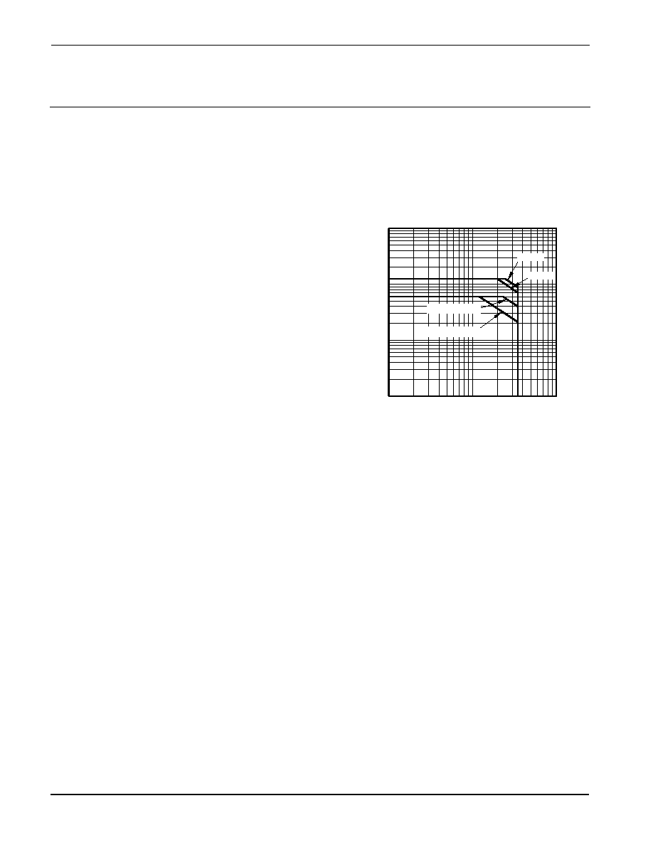
PHASE COMPENSATION
Open loop gain and phase shift both increase with increas-
ing temperature. The PHASE COMPENSATION typical graph
shows closed loop gain and phase compensation capacitor
value relationships for four case temperatures. The curves
are based on achieving a phase margin of 50∞. Calculate
the highest case temperature for the application (maximum
ambient temperature and highest internal power dissipation)
before choosing the compensation. Keep in mind that when
working with small values of compensation, parasitics may
play a large role in performance of the finished circuit. The
compensation capacitor must be rated for at least the total
voltage applied to the amplifier and should be a temperature
stable type such as NPO or COG.
OTHER STABILITY CONCERNS
There are two important concepts about closed loop gain
when choosing compensation. They stem from the fact that
while "gain" is the most commonly used term,
(the feedback
factor) is really what counts when designing for stability.
1. Gain must be calculated as a non-inverting circuit (equal
input and feedback resistors can provide a signal gain of
-1, but for calculating offset errors, noise, and stability, this
is a gain of 2).
2. Including a feedback capacitor changes the feedback factor
or gain of the circuit. Consider Rin=4.7k, Rf=47k for a gain
of 11. Compensation of 4.7 to 6.8pF would be reasonable.
Adding 33pF parallel to the 47k rolls off the circuit at 103kHz,
and at 2MHz has reduced gain from 11 to roughly 1.5 and
the circuit is likely to oscillate.
As a general rule the DC summing junction impedance
(parallel combination of the feedback resistor and all input
resistors) should be limited to 5k ohms or less. The amplifier
input capacitance of about 6pF, plus capacitance of connecting
traces or wires and (if used) a socket will cause undesirable
circuit performance and even oscillation if these resistances
are too high. In circuits requiring high resistances, measure or
estimate the total sum point capacitance, multiply by Rin/Rf, and
parallel Rf with this value. Capacitors included for this purpose
are usually in the single digit pF range. This technique results
in equal feedback factor calculations for AC and DC cases. It
does not produce a roll off, but merely keeps
constant over
a wide frequency range. Paragraph 6 of Application Note 19
details suitable stability tests for the finished circuit.

APEX MICROTECHNOLOGY CORPORATION ∑ TELEPHONE (520) 690-8600 ∑ FAX (520) 888-3329 ∑ ORDERS (520) 690-8601 ∑ EMAIL prodlit@apexmicrotech.com
5
This data sheet has been carefully checked and is believed to be reliable, however, no responsibility is assumed for possible inaccuracies or omissions. All specifications are subject to change without notice.
PA240U REV B MARCH 2006 © 2006 Apex Microtechnology Corp.
FIGURE 1
OVERVOLTAGE PROTECTION
Although the PA240 can withstand differential input voltages
up to 16V, in some applications additional external protection
may be needed. Differential inputs exceeding 16V will be
clipped by the protection circuitry. However, if more than a few
milliamps of current is available from the overload source, the
protection circuitry could be destroyed. For differential sources
above 16V, adding series resistance limiting input current to
1mA will prevent damage. Alternatively, 1N4148 signal diodes
connected anti-parallel across the input pins is usually sufficient.
In more demanding applications where bias current is impor-
tant, diode connected JFETs such as 2N4416 will be required.
See Q1 and Q2 in Figure 1. In either case the differential input
voltage will be clamped to 0.7V. This is sufficient overdrive to
produce the maximum power bandwidth.
+Vs
-Vs
OUT
+Vs
-Vs
Z1
Z2
-IN
+IN
Q1
Q2
OPERATING
CONSIDERATIONS
PA240
In the case of inverting circuits where the +IN pin is grounded,
the diodes mentioned above will also afford protection from
excessive common mode voltage. In the case of non-invert-
ing circuits, clamp diodes from each input to each supply will
provide protection. Note that these diodes will have substantial
reverse bias voltage under normal operation and diode leak-
age will produce errors.
Some applications will also need over-voltage protection
devices connected to the power supply rails. Unidirectional
zener diode transient suppressors are recommended. The
zeners clamp transients to voltages within the power supply
rating and also clamp power supply reversals to ground.
Whether the zeners are used or not the system power supply
should be evaluated for transient performance including power-
on overshoot and power-off polarity reversals as well as line
regulation. See Z1 and Z2 in Figure 1.
APPLICATION REFERENCES:
For additional technical information please refer to the fol-
lowing Application Notes:
AN1: General Operating Considerations
AN3: Bridge Circuit Drives
AN25: Driving Capacitive Loads
AN38: Loop Stability with Reactive Loads