 | –≠–ª–µ–∫—Ç—Ä–æ–Ω–Ω—ã–π –∫–æ–º–ø–æ–Ω–µ–Ω—Ç: PA44U | –°–∫–∞—á–∞—Ç—å:  PDF PDF  ZIP ZIP |
APEX MICROTECHNOLOGY CORPORATION ∑ TELEPHONE (520) 690-8600 ∑ FAX (520) 888-3329 ∑ ORDERS (520) 690-8601 ∑ EMAIL prodlit@apexmicrotech.com
FEATURES
∑ SURFACE MOUNT PACKAGE
∑ MONOLITHIC MOS TECHNOLOGY
∑ LOW COST
∑ HIGH VOLTAGE OPERATION--350V
∑ LOW QUIESCENT CURRENT--2mA
∑ NO SECOND BREAKDOWN
∑ HIGH OUTPUT CURRENT--120 mA PEAK
APPLICATIONS
∑ TELEPHONE RING GENERATOR
∑ PIEZO ELECTRIC POSITIONING
∑ ELECTROSTATIC TRANSDUCER & DEFLECTION
∑ DEFORMABLE MIRROR FOCUSING
DESCRIPTION
The PA44 is a high voltage monolithic MOSFET operational
amplifier achieving performance features previously found
only in hybrid designs while increasing reliability. Inputs are
protected from excessive common mode and differential mode
voltages. The safe operating area (SOA) has no second
breakdown limitations and can be observed with all type loads
by choosing an appropriate current limiting resistor. External
compensation provides the user flexibility in choosing
optimum gain and bandwidth for the application.
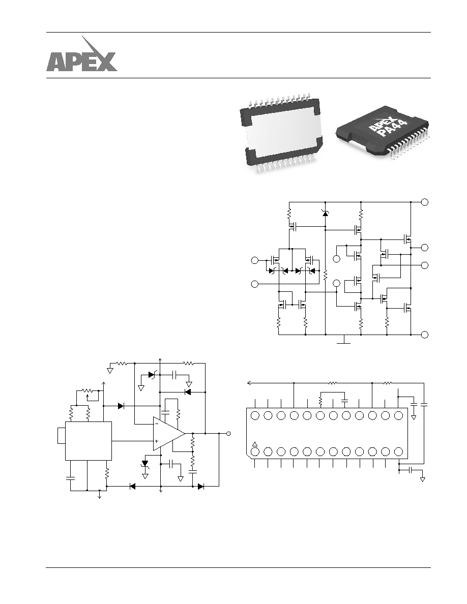
The PA44 is packaged in Apex's PSOP1 non-hermetic
surface mountable dual in line package. The metal back of the
package is tied to ≠Vs.
The PA44 is set for a gain of 38.5 boosting the 2.33V signal
to 90V. The recommended compensation for gains above 30
is used. If capacitive loading is at least 330pF at all times, the
recommended snubber network may be omitted. The 27 ohm
resistor sets current limit to a nominal value of 111mA to insure
peak currents out of at least 78mA.
Telephone Ring Generator
PHASE COMPENSATION
Gain
C
C
R
C
1
18pF
2.2K
10
10pF
2.2K
30
3.3pF
2.2K
EXTERNAL CONNECTIONS
EQUIVALENT SCHEMATIC
TYPICAL APPLICATION
H T T P : / / W W W . A P E X M I C R O T E C H . C O M ( 8 0 0 ) 5 4 6 - A P E X ( 8 0 0 ) 5 4 6 - 2 7 3 9
M I C R O T E C H N O L O G Y
HIGH VOLTAGE POWER OPERATIONAL AMPLIFIER
PA44
≠IN
OUT
+V
S
≠V
S
+IN
D2
D3
D4
D5
Q5
Q4
5
7
12
21
15
13
Q1
Q11
Q12
D1
Q2
Q6
Q8
Q13
SUB
Q14
Q10
Q9
Q7
Q3
I
LIM
COMP
COMP
19
17
TOP VIEW
OUT
COMP
COMP
100
13
15
17
19
21
12
1
5
7
≠IN
NC
+IN
≠V
S
+V
S
C
C
R
C
Rc
L
Rs
I
LIM
*
330pF
C
S
*
*
Supply bypassing required. See General Operating Considerations.
MUR120
IN6300A
.22
27
100
330pf
2.2K
3.3pF
.22
100K
2.67K
2.5K + 15
10K
10K
ICL8038
11
10
8
7
2
6
5
4
PA44
MUR130
IN6300A
90Vrms
82K
*
140V
≠140V
≠15V
* 1.5
µ
F @ 16Hz
1.2
µ
F @ 20Hz
15V
MUR120
MUR130
APEX MICROTECHNOLOGY CORPORATION ∑ 5980 NORTH SHANNON ROAD ∑ TUCSON, ARIZONA 85741 ∑ USA ∑ APPLICATIONS HOTLINE: 1 (800) 546-2739
PARAMETER
TEST CONDITIONS
1
MIN
TYP
MAX
UNITS
INPUT
OFFSET VOLTAGE, initial
4
15
30
mV
OFFSET VOLTAGE, vs. temperature
4
Full temperature range
70
130
µV/∞C
OFFSET VOLTAGE, vs supply
20
32
µV/V
OFFSET VOLTAGE, vs time
75
µV kh
BIAS CURRENT, initial
50
200
pA
BIAS CURRENT, vs supply
2
20
pA/V
OFFSET CURRENT, initial
50
200
pA
INPUT IMPEDANCE, DC
10
11
INPUT CAPACITANCE
5
pF
COMMON MODE, voltage range
±V
S
≠12
V
COMMON MODE REJECTION, DC
V
CM
= ±90V DC
84
94
dB
NOISE, broad band
10kHz BW, R
S
= 1K
50
µV RMS
NOISE, low frequency
1-10 Hz
110
µV p-p
GAIN
OPEN LOOP at 15Hz
R
L
= 5K
94
106
dB
BANDWIDTH, open loop
1.6
MHz
POWER BANDWIDTH
C
C
= 10pf, 280V p-p
26
kHz
PHASE MARGIN
Full temperature range
60
∞
OUTPUT
VOLTAGE SWING
I
O
= 40mA
±V
S
≠12
±V
S
≠10
V
CURRENT, peak
5
120
mA
CURRENT, continuous
60
mA
SETTLING TIME to .1%
C
C
= 10pF, 10V step, A
V
= ≠10
12
µs
SLEW RATE
C
C
= OPEN
40
V/µs
CAPACITIVE LOAD
A
V
= +1
10
nF
RESISTANCE
6
, no load
R
CL
= 0
150
RESISTANCE
6
, 20mA load
R
CL
= 0
25
POWER SUPPLY
VOLTAGE
3
See Note 3
±50
±150
±175
V
CURRENT, quiescent
1.6
2.0
mA
THERMAL
RESISTANCE, AC junction to case
F > 60Hz
6
7
∞C/W
RESISTANCE, DC junction to case
F < 60Hz
9
11
∞C/W
RESISTANCE, junction to air
Full temperature range
25
∞C/W
TEMPERATURE RANGE, case
Meets full range specifications
≠25
+85
∞C
ABSOLUTE MAXIMUM RATINGS
SPECIFICATIONS
PA44
ABSOLUTE MAXIMUM RATINGS
SUPPLY VOLTAGE, +V
S
to ≠V
S
350V
OUTPUT CURRENT, continuous within SOA
60 mA
OUTPUT CURRENT, peak
120 mA
POWER DISSIPATION, continuous @ T
C
= 25∞C
12W
INPUT VOLTAGE, differential
±16 V
INPUT VOLTAGE, common mode
±V
S
TEMPERATURE, pin solder ≠ 10 sec
220∞C
TEMPERATURE, junction
2
150∞C
TEMPERATURE, storage
≠65 to +150∞C
TEMPERATURE RANGE, powered (case)
≠40 to +125∞C
CAUTION
The PA44 is constructed from MOSFET transistors. ESD handling procedures must be observed.
SPECIFICATIONS
NOTES: 1.
Unless otherwise noted T
C
= 25∞C, C
C
= 18pF, R
C
= 2.2K. DC input specifications are ± value given. Power supply voltage is
typical rating.
2.
Long term operation at the maximum junction temperature will result in reduced product life. Derate internal power dissipation
to achieve high MTTF.
3.
Derate maximum supply voltage .5 V/∞C below case temperature of 25∞C. No derating is needed above T
C
= 25∞C.
4.
Sample tested by wafer to 95%.
5.
Guaranteed but not tested.
6.
The selected value of R
CL
must be added to the values given for total output resistance.
PA44
APEX MICROTECHNOLOGY CORPORATION ∑ TELEPHONE (520) 690-8600 ∑ FAX (520) 888-3329 ∑ ORDERS (520) 690-8601 ∑ EMAIL prodlit@apexmicrotech.com
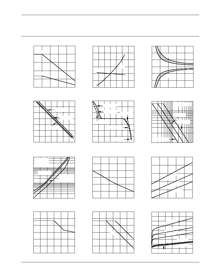
TYPICAL PERFORMANCE
GRAPHS
PA44
CURRENT LIMIT RESISTOR, R
CL
( )
0
25
50
75
100
125
TEMPERATURE, T (∞C)
0
3
6
POWER DERATING
INTERNAL POWER DISSIPATION, P(W)
≠50
0
100
80
100
130
140
CURRENT LIMIT
110
90
100
150
300
350
TOTAL SUPPLY VOLTAGE, V
S
(V)
NORMALIZED QUIESCENT CURRENT, (%)
1
100
10M
FREQUENCY, F (Hz)
≠20
0
60
120
SMALL SIGNAL RESPONSE
OPEN LOOP GAIN, A(dB)
20
40
80
100
1
100
.1M
10M
≠210
≠150
≠60
0
PHASE RESPONSE
≠90
≠30
10K
20K
.2M
.1M
FREQUENCY, F (Hz)
20
OUTPUT VOLTAGE, V (V )
O
1
100
1K
1M
FREQUENCY, F (Hz)
0
80
120
COMMON MODE REJECTION
COMMON MODE REJECTION, CMR (dB)
20
60
100
1
1M
FREQUENCY, F (Hz)
0
20
120
POWER SUPPLY REJECTION
POWER SUPPLY REJECTION, PSR (dB)
40
100
0
40
60
OUTPUT CURRENT, I
O
(mA)
2
10
OUTPUT VOLTAGE SWING
VOLTAGE DROP FROM SUPPLY, V
S
≠ V
O
(V)
4
8
100
10K
FREQUENCY, F (Hz)
.002
HARMONIC DISTORTION
DISTORTION, (%)
.02
1.0
30K
200
1K
0
COMPENSATION CAPACITANCE, C
C
(pf)
SLEW RATE
SLEW RATE, V/
µ
s
0
300
400
≠60
40
CURRENT LIMIT
CURRENT LIMIT RANGE, I (mA)
20
10
10K
.1M
20
120
0
QUIESCENT CURRENT
200
50
70
90
1K
≠25
25
50
75
120
15
POWER RESPONSE
PP
30K
10
100
1K
10K .1M
80
100
200
≠40
≠20
0
10
1K
10K .1M 1M
9
12
10
10K
1M
FREQUENCY, F (Hz)
PHASE, (
∞
)
NORMALIZED CURRENT LIMIT, (%)
0
3K
100K
.004
.04
4
20
8
16
12
10
20
30
40
50
60
40
60
80
100
200
400
40
80
60
T = T
125
+I
LIM
500
60
CASE TEMPERATURE, T (∞C)
C
≠180
≠120
110
130
150
6
-I
LIM
C
C
= 18pF
C
C
= 10pF
C
C
= 3.3pF
C
C
= 18pF
C
C
= 18pF
C
C
= 10pF
C
C
= 3.3pF
C
C
= 3.3pF
C
C
= 10pF
50K
.3M .5M
1M
C
C
= 10pF
C
C
= 3.3pF
C
C
= 18pF
R
L
= 10K
.006
.01
.06
.1
.2
.4
.6
≠I
LIM
+I
LIM
250
T
C
= -25
∞C
T
C
= 25
∞C
T
C
= 85
∞C
12
100
V
O
= 180V
PP
V
O
= 60V
PP
V
O
= 30V
PP
A
V
= 20
C
C
= 3.3pf
R
L
= 2K
+V
S
≠V
S
T = T
A
C
25∞C ≠
OUT
≠25∞C +OUT
85∞C ≠
OUT
≠25∞C ≠
OUT
85∞C +OUT
25∞C +OUT
14
16
18
APEX MICROTECHNOLOGY CORPORATION ∑ 5980 NORTH SHANNON ROAD ∑ TUCSON, ARIZONA 85741 ∑ USA ∑ APPLICATIONS HOTLINE: 1 (800) 546-2739
OPERATING
CONSIDERATIONS
PA44
GENERAL
Please read Application Note 1 "General Operating Consid-
erations" which covers stability, supplies, heat sinking, mount-
ing, current limit, SOA interpretation, and specification inter-
pretation. Visit www.apexmicrotech.com for design tools that
help automate tasks such as calculations for stability, internal
power dissipation, current limit; heat sink selection; Apex's
complete Application Notes library; Technical Seminar Work-
book; and Evaluation Kits.
CURRENT LIMIT
For proper operation the current limit resistor, R
CL
, must be
connected as shown in the external connection diagram. The
minimum value is 18 ohms, however for optimum reliability the
resistor value should be set as high as possible. The value can
be estimated as follows with the maximum practical value of
500 ohms.
3
R
CL
=
I
LIM
Use the typical performance graphs as a guide for expected
variations in current limit value with a given R
CL
and variations
over temperature. The selected value of R
CL
must be added to
the specified typical value of output resistance to calculate the
total output resistance. Since the load current passes through
R
CL
the value selected also affects the output voltage swing
according to:
V
R
= I
O
R
CL
where V
R
is the voltage swing reduction.
When the amplifier is current limiting, there may be small
signal spurious oscillation present during the current limited
portion of the negative half cycle. The frequency of the oscil-
lation is not predictable and depends on the compensation,
gain of the amplifier, and load. The oscillation will cease as the
amplifier comes out of current limit.
INPUT PROTECTION
The PA44 inputs are protected against common mode
voltages up the supply rails and differential voltages up to ±16
volts as well as static discharge. Differential voltages exceed-
ing 16 volts will be clipped by the protection circuitry. However,
if more than a few milliamps of current is available from the
overload source, the protection circuitry could be destroyed.
The protection circuitry includes 300 ohm current limiting
resistors at each input, but this may be insufficient for severe
overloads. It may be necessary to add external resistors to the
application circuit where severe overload conditions are ex-
pected. Limiting input current to 1mA will prevent damage.
STABILITY
The PA44 has sufficient phase margin when compensated
for unity gain to be stable with capacitive loads of at least 10 nF.
However, the low pass circuit created by the sumpoint (≠in)
capacitance and the feedback network may add phase shift
and cause instabilities. As a general rule, the sumpoint load
resistance (input and feedback resistors in parallel) should be
1K ohm or less at low gain settings (up to 10). Alternatively, use
*
a bypass capacitor across the feedback resistor. The time
constant of the feedback resistor and bypass capacitor com-
bination should match the time constant of the sumpoint
resistance and sumpoint capacitance.
The PA44 is externally compensated and performance can
be tailored to the application. Use the graphs of small signal
gain and phase response as well as the graphs for slew rate
and power response as a guide. The compensation capacitor
C
C
must be rated at 350V working voltage. The compensation
capacitor and associated resistor R
C
must be mounted closely
to the amplifier pins to avoid spurious oscillation. An NPO
capacitor is recommended for compensation.
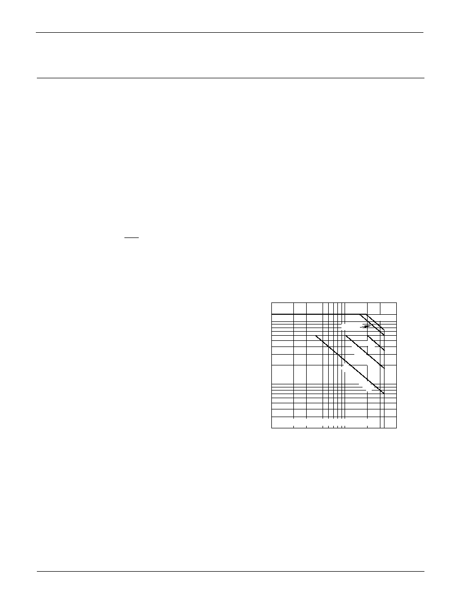
SAFE OPERATING AREA (SOA)
The MOSFET output stage of this power operational ampli-
fier has two distinct limitations:
1. The current handling capability of the die metallization.
2. The temperature of the output MOSFETs.
NOTE: The output stage is protected against transient
flyback. However, for protection against sustained, high en-
ergy flyback, external fast-recovery diodes should be used.
SUPPLY TO OUTPUT DIFFERENTIAL, V
S
-V
O
(V)
10
20
30
50
100
200
300
500
OUTPUT CURRENT FROM +V
S
OR ≠V
S
, (mA)
2
3
4
5
10
20
30
40
50
100
DC, T
C
= 125
∞C
DC, T
C
= 85
∞C
DC
300mS
PULSE CURVES @ 10% DUTY CYCLE MAX
PA44 SOA
200mS
120
200
HEATSINKING
The PA44 package has a large exposed integrated copper
heatslug to which the monolithic amplifier is directly attached.
The solder connection of the heatslug to a minimum 1 square
inch foil area of the printed circuit board will result in thermal
performance of 25∞C/W junction to air rating of the PA44.
Solder connection to an area of 1 to 2 square inches of foil is
recommended. This may be adequate heatsinking but the
large number of variables involved suggest temperature mea-
surements be made on the top of the package. Do not allow the
temperature to exceed 85∞C. The heatslug is tied internally to ≠Vs.
This data sheet has been carefully checked and is believed to be reliable, however, no responsibility is assumed for possible inaccuracies or omissions. All specifications are subject to change without notice.
PA44U REV. E AUGUST 2001
© 2001 Apex Microtechnology Corp.