 | –≠–ª–µ–∫—Ç—Ä–æ–Ω–Ω—ã–π –∫–æ–º–ø–æ–Ω–µ–Ω—Ç: PA45A | –°–∫–∞—á–∞—Ç—å:  PDF PDF  ZIP ZIP |
APEX MICROTECHNOLOGY CORPORATION ∑ TELEPHONE (520) 690-8600 ∑ FAX (520) 888-3329 ∑ ORDERS (520) 690-8601 ∑ EMAIL prodlit@apexmicrotech.com
215
D
NO LONGER SUPPORTED FOR DESIGN-IN
FEATURES
∑ MONOLITHIC MOS TECHNOLOGY
∑ LOW COST
∑ HIGH VOLTAGE OPERATION--150V
∑ HIGH SLEW RATE--27V/µs
∑ HIGH POWER--5A, 85W DISSIPATION
APPLICATIONS
∑ MAGNETIC DEFLECTION
∑ PA AUDIO
∑ MOTOR DRIVE
∑ NOISE CANCELLATION
DESCRIPTION
The PA45 is a high power monolithic MOSFET operational
amplifier that achieves performance levels unavailable even in
many hybrid amplifier designs. Inputs are protected from
excessive common mode and differential mode voltages as
well as static discharge. The safe operating area (SOA) has no
second breakdown limitations and can be observed with all
type loads by choosing an appropriate current limiting resistor.
External compensation provides the user flexibility in choosing
optimum gain and bandwidth for the application.
This circuit utilizes a beryllia (BeO) substrate to minimize
thermal resistance. Ultrasonically bonded aluminum wires
provide reliable interconnections at all operating tempera-
tures. The 8-pin TO-3 package is hermetically sealed and
electrically isolated. The use of compressible isolation wash-
ers and/or improper mounting torque will void the product
warranty.
EQUIVALENT SCHEMATIC
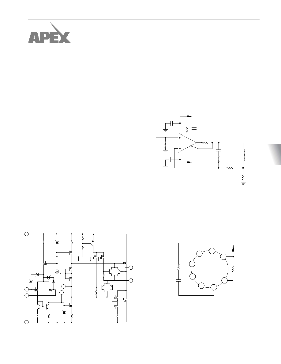
TYPICAL APPLICATION
PA45
+80
R
C
C
C
R
CL
R
I
≠20
C
F
R
D
R
F
R
S
YOKE
V
I
±2.5A 7µSec Retrace
Horizontal Deflection Coil Amplifiers
1
6
5
4
3
2
7
8
Horizontal deflection amplifiers require both high speed and
low distortion. The speed at which current can be changed in a
deflection coil is a function of the voltage available from the op
amp. In this application an 80 volt power supply is used for the
retrace polarity to provide a 7
µ
Sec retrace time, half of which is
required for amplifier slewing. This circuit can perform 15.75
KHz deflection in up to 50
µ
H coils at up to 5A p-p.
PHASE
COMPENSATION
Gain
C
C
R
C
10
10pF
1K
1
68pF
1K
CC1
CC2
2
7
3
5
4
6
8
1
Q19
Q17
Q16
Q15
Q14
Q9
Q10
Q7
D7
Q21
Q20
≠V
S
+IN
≠IN
Q11
Q12
D4
D2
Q3
D3
D5
Q8
Q13
Q24
D1
Q2
Q5
Q6
+V
S
CURRENT
SENSE
OUTPUT
DRIVE
PATENTED
EXTERNAL CONNECTIONS
TOP VIEW
1
2
3
4
5
6
7
8
+IN
≠V
S
OUTPUT
DRIVE
≠IN
CC2
C IS NPO RATED
FOR FULL SUPPLY VOLTAGE.
R
CL
C
OUTPUT
CURRENT
SENSE
CC1
+V
S
C
C
R
C
H T T P : / / W W W . A P E X M I C R O T E C H . C O M ( 8 0 0 ) 5 4 6 - A P E X ( 8 0 0 ) 5 4 6 - 2 7 3 9
M I C R O T E C H N O L O G Y
HIGH VOLTAGE POWER OPERATIONAL AMPLIFIER
PA45

APEX MICROTECHNOLOGY CORPORATION ∑ 5980 NORTH SHANNON ROAD ∑ TUCSON, ARIZONA 85741 ∑ USA ∑ APPLICATIONS HOTLINE: 1 (800) 546-2739
216
NO LONGER SUPPORTED FOR DESIGN-IN
ABSOLUTE MAXIMUM RATINGS
SPECIFICATIONS
PA45
ABSOLUTE MAXIMUM RATINGS
SUPPLY VOLTAGE, +V
S
to ≠V
S
150V
OUTPUT CURRENT, continuous within SOA
5A
POWER DISSIPATION, continuous @ T
C
= 25
∞
C
85W
INPUT VOLTAGE, differential
±
16 V
INPUT VOLTAGE, common mode
±
V
S
TEMPERATURE, pin solder ≠ 10 sec
300
∞
C
TEMPERATURE, junction
150
∞
C
TEMPERATURE, storage
≠65 to +150
∞
C
TEMPERATURE RANGE, powered (case)
≠55 to +125
∞
C
PARAMETER
TEST CONDITIONS
1
MIN
TYP
MAX
UNITS
INPUT
OFFSET VOLTAGE, initial
5
10
mV
OFFSET VOLTAGE, vs. temperature
Full temperature range
10
50
µ
V/
∞
C
OFFSET VOLTAGE, vs supply
8
15
µ
V/V
OFFSET VOLTAGE, vs time
2
µ
V
kh
BIAS CURRENT, initial
20
100
pA
BIAS CURRENT, vs supply
2
pA/V
OFFSET CURRENT, initial
200
pA
INPUT IMPEDANCE, DC
10
11
INPUT CAPACITANCE
5
pF
COMMON MODE, voltage range
±
V
S
≠10
V
COMMON MODE REJECTION, DC
90
106
dB
NOISE, broad band
10kHz BW, R
S
= 1K
10
µ
V RMS
GAIN
OPEN LOOP at 15Hz
94
106
dB
GAIN BANDWIDTH PRODUCT @ 1MHz
R
L
= 500
, C
C
= 10pF
4.5
MHz
POWER BANDWIDTH
C
C
= 10pF, 130V p-p, R
L
= 8
66
kHz
PHASE MARGIN
Full temp range, C
C
= 68pF, R
L
= 10
60
∞
OUTPUT
VOLTAGE SWING
I
O
= 5A
±
V
S
≠10
±
V
S
≠8
V
CURRENT, continuous
5
A
SETTLING TIME to .1%
10V step, A
V
= ≠10
2
µ
s
SLEW RATE
C
C
= 10pF, R
L
= 8
27
V/
µ
s
CAPACITIVE LOAD
A
V
= +1, C
C
= 68pF
10
nF
RESISTANCE , no load
R
CL
= 0
150
POWER SUPPLY
VOLTAGE
3
See Note 3
±
15
±
50
±
75
V
CURRENT, quiescent
30
50
mA
THERMAL
2
RESISTANCE, AC junction to case
F > 60Hz
1.3
∞
C/W
RESISTANCE, DC junction to case
F < 60Hz
1.5
∞
C/W
RESISTANCE, junction to air
Full temperature range
30
∞
C/W
TEMPERATURE RANGE, case
Meets full range specifications
≠25
+85
∞
C
SPECIFICATIONS
CAUTION
The PA45 is constructed from MOSFET transistors. ESD handling procedures must be observed.
The internal substrate contains beryllia (BeO). Do not break the seal. If accidentally broken, do not crush, machine, or
subject to temperatures in excess of 850
∞
C to avoid generating toxic fumes.
NOTES: 1.
Unless otherwise noted T
C
= 25
∞
C, C
C
= 10pF, R
C
= 1K
. DC input specifications are
±
value given. Power supply voltage is
typical rating.
2.
Long term operation at the maximum junction temperature will result in reduced product life. Derate internal power dissipation
to achieve high MTTF. For guidance, refer to heatsink data sheet.
3.
Derate maximum supply voltage .5 V/
∞
C below case temperature of 25
∞
C. No derating is needed above T
C
= 25
∞
C.

APEX MICROTECHNOLOGY CORPORATION ∑ TELEPHONE (520) 690-8600 ∑ FAX (520) 888-3329 ∑ ORDERS (520) 690-8601 ∑ EMAIL prodlit@apexmicrotech.com
217
D
NO LONGER SUPPORTED FOR DESIGN-IN
TYPICAL PERFORMANCE
GRAPHS
PA45
CURRENT LIMIT RESISTOR, R
CL
(
)
0
25
50
75
100
125
CASE TEMPERATURE, T
C
(
∞
C)
0
20
40
POWER DERATING
INTERNAL POWER DISSIPATION, P(W)
≠50
0
100
0.7
0.8
0.9
1.0
1.1
1.2
CURRENT LIMIT DRIFT
10
30
90
150
130
110
TOTAL SUPPLY VOLTAGE, V
S
(V)
NORMALIZED QUIESCENT CURRENT, I
Q
(X)
.1
1
100
10M
FREQUENCY, f (Hz)
0
120
SMALL SIGNAL RESPONSE
OPEN LOOP GAIN, A(dB)
40
80
1
.1
100
100K
10M
≠180
≠135
≠45
0
PHASE RESPONSE
≠90
10K
20K
200K
100K
FREQUENCY, f (Hz)
4
6
OUTPUT VOLTAGE, V (V )
O
10
1K
10K
1M
FREQUENCY, f (Hz)
80
COMMON MODE REJECTION
COMMON MODE REJECTION, CMR (dB)
20
60
100
1M
FREQUENCY, f (Hz)
0
20
120
POWER SUPPLY REJECTION
POWER SUPPLY REJECTION, PSR (dB)
40
100
0
2
OUTPUT CURRENT, I
O
(A)
2
OUTPUT VOLTAGE SWING
VOLTAGE DROP FROM SUPPLY, V
S
≠ V
O
(V)
4
10
1K 2K 4K
FREQUENCY, f (Hz)
.001
HARMONIC DISTORTION
DISTORTION, THD (%)
.020
1.000
10K
40
20
100
0
COMPENSATION CAPACITANCE, C
C
(pF)
SLEW RATE
SLEW RATE, SR(V/
µ
s)
0.1
4
ABSOLUTE CURRENT LIMIT
CURRENT LIMIT, I (A)
100
100K
QUIESCENT CURRENT
50
0.5
1.0
1K
≠25
25
50
75
100
POWER RESPONSE
PP
10
100
1K
10K
100K
80
1.0
≠4
10
10
1K 10K 100K 1M
60
80
10
10K
1M
FREQUENCY, f (Hz)
PHASE, (
∞
)
NORMALIZED CURRENT LIMIT, I
LIM
(X)
0
400
20K
.002
.040
20
80
60
40
20
30
40
50
8
10
20
40
60
80
100
200
40
60
125
+I
LIM
10
CASE TEMPERATURE, T (
∞
C)
C
1.5
2.0
6
-I
LIM
40K
400K
1M
.004
.010
.100
.200
.400
70
8
4
10
T
C
= 25
∞
C
T
C
= ≠55
∞
C
T
C
= +125
∞
C
No Load
8
Load
A
V
= 10
C
C
= 10pf
R
L
= 8
85W
5W
1W
C
C
= 68pF
C
C
= 10pF
C
C
= 68pF
C
C
= 10pF
+V
S
≠V
S
85
∞
C +OUT
85
∞
C ≠ OUT
25
∞
C ≠ OUT
25
∞
C +OUT
R
L
= 8
C
C
= 10pF
C
C
= 68pF
R
L
= 500
R
L
= 1K
R
L
= 500
APEX MICROTECHNOLOGY CORPORATION ∑ 5980 NORTH SHANNON ROAD ∑ TUCSON, ARIZONA 85741 ∑ USA ∑ APPLICATIONS HOTLINE: 1 (800) 546-2739
218
NO LONGER SUPPORTED FOR DESIGN-IN
OPERATING
CONSIDERATIONS
PA45
GENERAL
Please read Application Note 1 "General Operating Consid-
erations" which covers stability, supplies, heat sinking, mount-
ing, current limit, SOA interpretation, and specification inter-
pretation. Visit www.apexmicrotech.com for design tools that
help automate tasks such as calculations for stability, internal
power dissipation, current limit; heat sink selection; Apex's
complete Application Notes library; Technical Seminar Work-
book; and Evaluation Kits.
CURRENT LIMIT
Current limiting is achieved by developing 0.83V on the
amplifiers current sense circuit by way of an internal tie to the
output drive (pin 8) and an external current sense line (pin 1).
A sense resistor R
CL
is used to relate this sense voltage to a
current flowing from output drive.
0.83 ≠ 0.05 * I
CL
R
CL
=
I
CL
0.83
I
CL
=
R
CL
+ 0.05
with a maximum practical value of 16
. R
CL
is added to the
typical value of output resistance and affects the total possible
swing since it carries the load current. The swing reduction, V
R
can be established V
R
= I
OUT
*
R
CL
.
INPUT PROTECTION
The PA45 inputs are protected against common mode
voltages up to the supply rails, differential voltages up to
±
16
volts and static discharge. Differential voltages exceeding 16
volts will be clipped by the protection circuitry. However, if
more than a few milliamps of current is available from the input
drive source, the protection circuitry could be destroyed. The
protection circuitry includes 300 ohm current limiting resistors
at each input. This security may be insufficient for severe
overdrive of the input. Adding external resistors to the applica-
tion which limits severe input overdrive current to 1mA, will
prevent damage.
STABILITY
The PA45 has sufficient phase margin when compensated
for unity gain to be stable with capacitive loads of at least 10nF.
However, the low pass circuit created by the sum-point (≠in)
capacitance and the feedback network may add phase shift
and cause instabilities. As a rule, the sum-point load resis-
tance (input and feedback resistors in parallel) should be 1k
ohm or less. Alternatively, use a bypass capacitor across the
feedback resistor. The time constant of the feedback resistor
and bypass capacitor combination should match the time
constant of the sum-point resistance and sum-point capaci-
tance.
The PA45 is externally compensated and performance can
be tailored to the application. The compensation network C
C
-
R
C
must be mounted closely to the amplifier pins 7 and 2 to
avoid noise coupling to these high impedance nodes.
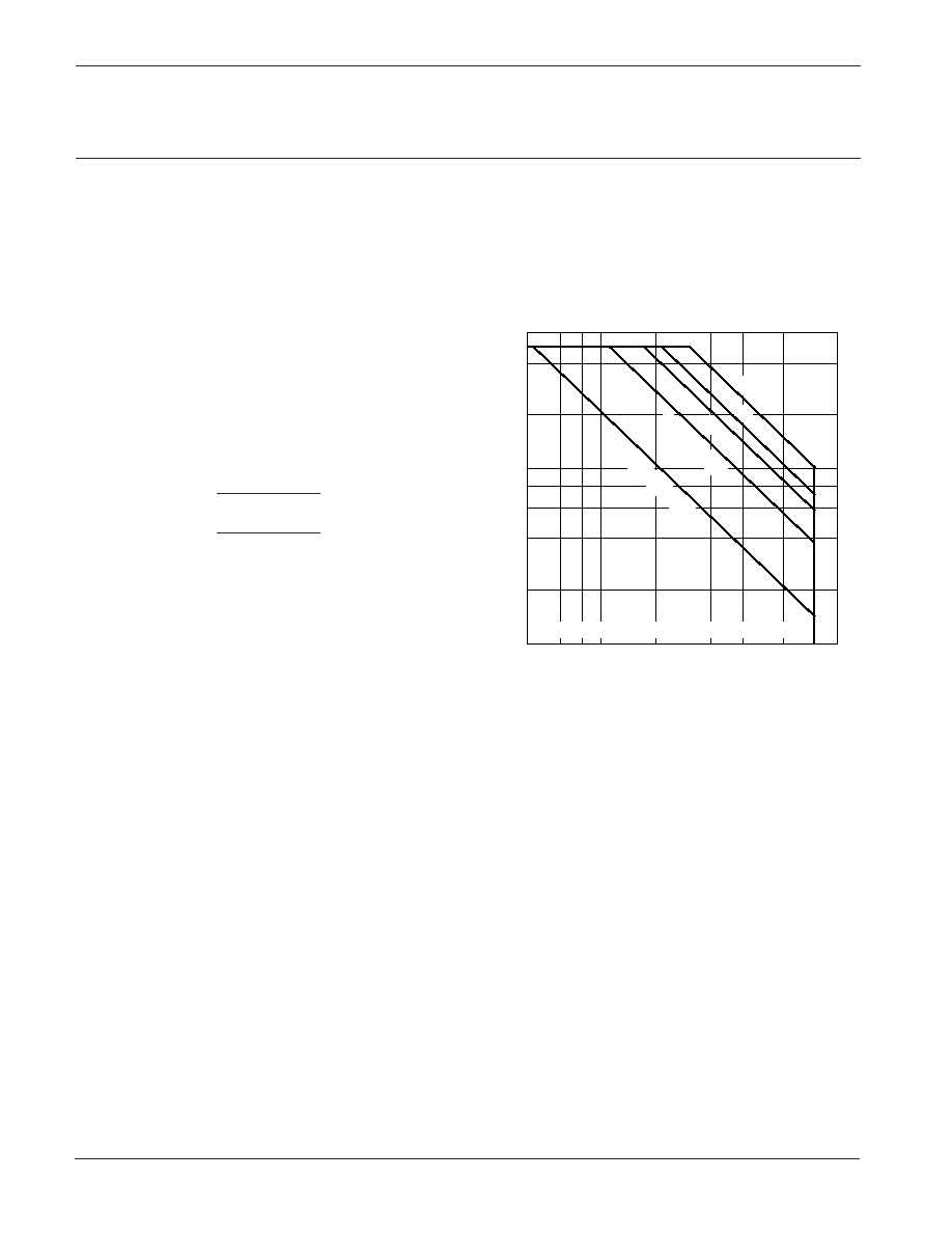
SAFE OPERATING AREA (SOA)
The MOSFET output stage of this power operational ampli-
fier has limitations from its channel temperature.
NOTE: The output is protected against transient flyback.
However, for protection against sustained, high energy flyback,
external fast-recovery diodes should be used.
SUPPLY TO OUTPUT DIFFERENTIAL, V
S
-V
O
(V)
4
6
8 10
20
40
60
100
200
OUTPUT CURRENT FROM +V
S
OR ≠V
S
, (A)
0.1
0.2
0.4
0.6
0.8
1.0
2.0
DC, T
C
= 85
∞
C
4.0
6.0
PULSE CURVES @ 10% DUTY CYCLE MAX
DC, T
C
= 125
∞
C
200mS
DC
100mS
SAFE OPERATING AREA
This data sheet has been carefully checked and is believed to be reliable, however, no responsibility is assumed for possible inaccuracies or omissions. All specifications are subject to change without notice.
PA45U REV. B FEBRUARY 1998
© 1998 Apex Microtechnology Corp.