 | –≠–Ľ–Ķ–ļ—ā—Ä–ĺ–Ĺ–Ĺ—č–Ļ –ļ–ĺ–ľ–Ņ–ĺ–Ĺ–Ķ–Ĺ—ā: PA98 | –°–ļ–į—á–į—ā—Ć:  PDF PDF  ZIP ZIP |

APEX MICROTECHNOLOGY CORPORATION ∑ TELEPHONE (520) 690-8600 ∑ FAX (520) 888-3329 ∑ ORDERS (520) 690-8601 ∑ EMAIL prodlit@apexmicrotech.com
1
FEATURES
∑ HIGH VOLTAGE -- 450V (Ī225V)
∑ HIGH SLEW RATE -- 1000V/S
∑ HIGH OUTPUT CURRENT -- 200mA
APPLICATIONS
∑ HIGH VOLTAGE INSTRUMENTATION
∑ PIEZO TRANSDUCER EXCITATION
∑ PROGRAMMABLE POWER SUPPLIES UP TO 430V
∑ ELECTROSTATIC TRANSDUCERS & DEFLECTION
DESCRIPTION
The PA98 is a high voltage, high power bandwidth MOSFET
operational amplifier designed for output currents up to 200mA.
Output voltages can swing up to Ī215V with a dual supply
and up to +440 volts with a single supply. The safe operating
area (SOA) has no second breakdown limitations and can
be observed with all types of loads by choosing an appropri-
ate current limiting resistor. High accuracy is achieved with
a cascode input circuit configuration. All internal biasing is
referenced to a bootstrapped zener-MOSFET current source.
As a result, the PA98 features an unprecedented supply range
and excellent supply rejection. The MOSFET output stage is
biased on for linear operation. External compensation provides
user flexibility.
This hybrid circuit utilizes thick film (cermet) resistors, ceramic
capacitors and silicon semiconductor chips to maximize reli-
ability, minimize size and give top performance. Ultrasonically
bonded aluminum wires provide reliable interconnections at
all operating temperatures. The Power SIP package is electri-
cally isolated.
EQUIVALENT SCHEMATIC
TYPICAL APPLICATION
DYNAMIC FOCUSING
Dynamic focusing is the active correction of focusing voltage
as a beam traverses the face of a CRT. This is necessary in
high resolution flat face monitors since the distance between
cathode and screen varies as the beam moves from the center
of the screen to the edges. PA98 lends itself well to this function
since it can be connected as a summing amplifier with inputs
from the nominal focus potential and the dynamic correction.
The nominal might be derived from a potentiometer, or per-
haps automatic focusing circuitry might be used to generate
this potential. The dynamic correction is generated from the
sweep voltages by calculating the distance of the beam from
the center of the display.
EXTERNAL CONNECTIONS
PHASE COMPENSATION
Gain
C
C
R
C
1
68pF
100
20
10pF
330
100
3.3pF
0
C
C
RATED FOR FULL SUPPLY VOLTAGE
PATENTED
12-PIN SIP
PACKAGE STYLE DP
Formed leads available
Package styles ED & EE

APEX MICROTECHNOLOGY CORPORATION ∑ 5980 NORTH SHANNON ROAD ∑ TUCSON, ARIZONA 85741 ∑ USA ∑ APPLICATIONS HOTLINE: 1 (800) 546-2739
2
ABSOLUTE MAXIMUM RATINGS
SPECIFICATIONS
PA98 ∑ PA98A
The PA98 is constructed from MOSFET transistors. ESD handling procedures must be observed.
The exposed substrate contains beryllia (BeO). Do not crush, machine, or subject to temperatures in excess of 850įC to
avoid generating toxic fumes.
CAUTION
ABSOLUTE MAXIMUM RATINGS
SUPPLY VOLTAGE, +V
S
to ≠V
S
450V
OUTPUT CURRENT, continuous within SOA
200mA
POWER DISSIPATION, continuous @ T
C
= 25įC
2
30W
INPUT VOLTAGE, differential
Ī25V
INPUT VOLTAGE, common mode
ĪV
S
TEMPERATURE, pin solder - 10s max.
260įC
TEMPERATURE, junction
2
150įC
TEMPERATURE RANGE, storage
≠40 to +85įC
OPERATING TEMPERATURE RANGE, case
≠25 to +85įC
SPECIFICATIONS
PA98
PA98A
PARAMETER
TEST CONDITIONS
1
MIN
TYP
MAX
MIN
TYP
MAX
UNITS
INPUT
OFFSET VOLTAGE, initial
.5
2
.25
.5
mV
OFFSET VOLTAGE, vs. temperature
Full temperature range
10
30
5
10
ĶV/įC
OFFSET VOLTAGE, vs. supply
3
10
*
*
ĶV/V
OFFSET VOLTAGE, vs. time
75
*
ĶV/kh
BIAS CURRENT, initial
3
5
50
3
10
pA
BIAS CURRENT, vs. supply
.01
*
pA/V
OFFSET CURRENT, initial
3
10
100
3
30
pA
INPUT IMPEDANCE, DC
10
11
*
INPUT CAPACITANCE
4
*
pF
COMMON MODE VOLTAGE RANGE
4
ĪV
S
≠15
*
V
COMMON MODE REJECTION, DC
V
CM
= Ī90V
90
110
*
*
dB
NOISE
100kHz BW, R
S
= 1K, C
C
= 10pf
1
*
ĶVrms
GAIN
OPEN LOOP, @ 15Hz
R
L
= 2K, C
C
= OPEN
96
111
*
*
dB
GAIN BANDWIDTH PRODUCT at 1MHz R
L
= 2K, C
C
= 3.3pf
100
*
MHz
POWER BANDWIDTH
C
C
= 10pf
300
*
kHz
C
C
= 3.3pf
500
*
kHz
PHASE MARGIN
Full temperature range
60
*
į
OUTPUT
VOLTAGE SWING
4
I
O
= Ī200mA
ĪVs≠10 ĪVs≠6.5
*
*
V
VOLTAGE SWING
4
I
O
= Ī75mA
ĪV≠8.5 ĪVs≠6.0
*
*
V
VOLTAGE SWING
4
I
O
= Ī20mA
ĪV≠8.0 ĪVs≠5.5
*
*
V
CURRENT, continuous
T
C
= 85įC
Ī200
*
mA
SLEW RATE, A
V
= 20
C
C
= 10pf
400
*
V/Ķs
SLEW RATE, A
V
= 100
C
C
= OPEN
1000
700
*
V/Ķs
CAPACITIVE LOAD, A
V
= +1
Full temperature range
470
*
*
pf
SETTLING TIME to .1%
C
C
= 10pf, 2V step
1
*
Ķs
RESISTANCE, no load
R
CL
= 0
50
*
POWER SUPPLY
VOLTAGE
6
Full temperature range
Ī15
Ī150
Ī225
*
*
*
V
CURRENT, quiescent
21
25
*
*
mA
THERMAL
RESISTANCE, AC, junction to case
5
Full temperature range, F > 60Hz
2.5
*
įC/W
RESISTANCE, DC, junction to case
Full temperature range, F < 60Hz
4.2
*
įC/W
RESISTANCE, junction to air
Full temperature range
30
*
įC/W
TEMPERATURE RANGE, case
Meets full range specifications
≠25
+85
*
*
įC
NOTES: * The specification of PA98A is identical to the specification for PA98 in applicable column to the left.
1. Unless otherwise noted: T
C
= 25įC, compensation = C
C
= 68pF, R
C
= 100. DC input specifications are Ī value given. Power
supply voltage is typical rating.
2. Long term operation at the maximum junction temperature will result in reduced product life. Derate internal power dissipation to
achieve high MTTF. Ratings apply only to output transistors. An additional 10W may be dissipated due to quiescent power.
3. Doubles for every 10įC of temperature increase.
4. +V
S
and ≠V
S
denote the positive and negative power supply rail respectively.
5. Rating applies if the output current alternates between both output transistors at a rate faster than 60Hz.
6. Derate max supply rating .625 V/įC below 25įC case. No derating needed above 25įC case.
APEX MICROTECHNOLOGY CORPORATION ∑ TELEPHONE (520) 690-8600 ∑ FAX (520) 888-3329 ∑ ORDERS (520) 690-8601 ∑ EMAIL prodlit@apexmicrotech.com
3
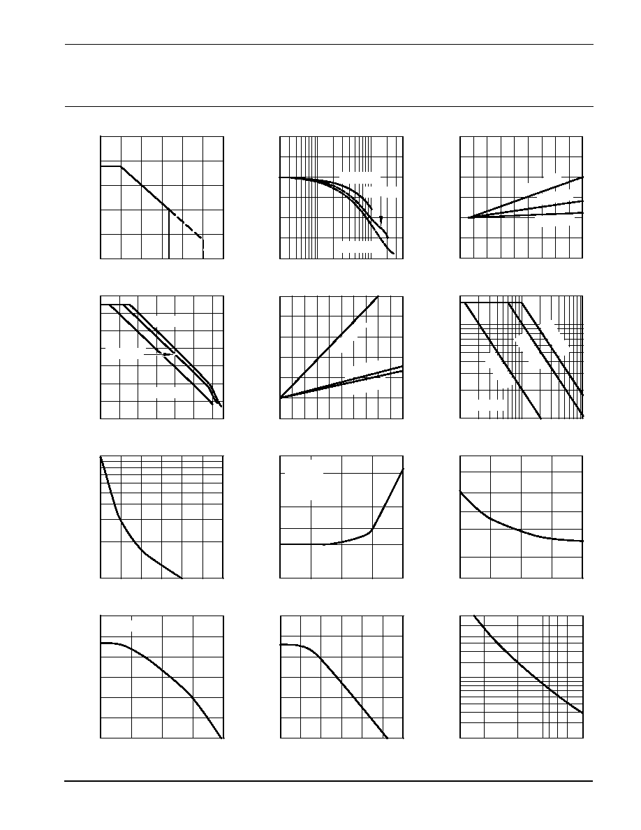
TYPICAL PERFORMANCE
GRAPHS
PA98 ∑ PA98A

APEX MICROTECHNOLOGY CORPORATION ∑ 5980 NORTH SHANNON ROAD ∑ TUCSON, ARIZONA 85741 ∑ USA ∑ APPLICATIONS HOTLINE: 1 (800) 546-2739
4
OPERATING
CONSIDERATIONS
PA98 ∑ PA98A
GENERAL
Please read Application Note 1 "General Operating Consider-
ations" which covers stability, supplies, heat sinking, mounting,
current limit, SOA interpretation, and specification interpreta-
tion. Visit www.apexmicrotech.com for design tools that help
automate tasks such as calculations for stability, internal power
dissipation, current limit; heat sink selection; Apex's complete
Application Notes library; Technical Seminar Workbook; and
Evaluation Kits.
CURRENT LIMIT
For proper operation, the current limit resistor (R
CL
) must be
connected as shown in the external connection diagram. The
minimum value is 1.4 ohm, however for optimum reliability the
resistor value should be set as high as possible. The value
is calculated as follows; with the maximum practical value of
30 ohms.
.7
R
CL
=
I
LIM
- .016
SAFE OPERATING AREA (SOA)
The MOSFET output stage of this power operational ampli-
fier has two distinct limitations:
1. The current handling capability of the MOSFET geometry
and the wire bonds.
2. The junction temperature of the output MOSFETs.
NOTE: The output stage is protected against transient flyback.
However, for protection against sustained, high energy flyback,
external fast-recovery diodes should be used.
SAFE OPERATING CURVES
The safe operating area curves define the maximum ad-
ditional internal power dissipation the amplifier can tolerate
when it produces the necessary output to drive an external
load. This is not the same as the absolute maximum internal
power dissipation listed elsewhere in the specification since
the quiescent power dissipation is significant compared to
the total.
INPUT PROTECTION
Although the PA98 can withstand differential voltages up to
Ī25V, additional external protection is recommended. Since
the PA98 is a high speed amplifier, low leakage, low capaci-
tance JFETs connected as diodes are recommended (e.g.
2N4416, Q1-Q4 in Figure 1). The differential input voltage will
be clamped to Ī1.4V. This is sufficient overdrive to produce
maximum power bandwidth.
POWER SUPPLY PROTECTION
Unidirectional zener diode transient suppressors are recom-
mended as protection on the supply pins. The zeners clamp
transients to voltages within the power supply rating and also
clamp power supply reversals to ground. Whether the zeners
are used or not, the system power supply should be evaluated
for transient performance including power-on overshoot and
power-off polarity reversals as well as line regulation.
Conditions which can cause open circuits or polarity reversals
on either power supply rail should be avoided or protected
against. Reversals or opens on the negative supply rail is
known to induce input stage failure. Unidirectional transzorbs
prevent this, and it is desirable that they be both electrically
and physically as close to the amplifier as possible.
STABILITY
The PA98 is externally compensated and performance can
be tailored to the application. Use the graphs of small signal
response and power response as a guide. The compensation
capacitor C
C
must be rated at 500V working voltage. An NPO
capacitor is recommended. The compensation network C
C
R
C
must be mounted closely to the amplifier pins 7 and 8 to avoid
spurious oscillation.

APEX MICROTECHNOLOGY CORPORATION ∑ TELEPHONE (520) 690-8600 ∑ FAX (520) 888-3329 ∑ ORDERS (520) 690-8601 ∑ EMAIL prodlit@apexmicrotech.com
5
This data sheet has been carefully checked and is believed to be reliable, however, no responsibility is assumed for possible inaccuracies or omissions. All specifications are subject to change without notice.
PA98U REV I DECEMBER 2004 © 2004 Apex Microtechnology Corp.
OPERATING
CONSIDERATIONS
PA98 ∑ PA98A
INTERNAL POWER DISSIPATION AND HEATSINK SELECTION
With the unique combination of high voltage and speed
of the PA98, traditional formulas for heatsink selection will
falsely lower the apparent power handling capability of this
amplifier. To more accurately predict operating temperatures
use Power Design
1
revision 10 or higher, or use the following
procedure:
Find internal dissipation (PD) resulting from driving the
load. Use Power Design or refer to Apex Applications Note
1, General Operating Considertaions, paragraph 7. Find total
quiescent power (PD
Q
) by multiplying 0.025A by V
SS
(total
supply voltage). Find output stage quiescent power (PD
QOUT
)
by multiplying 0.001 by V
SS
.
Calculate a heatsink rating which will maintain the case at
85įC or lower.
Where: T
C
= maximum case temperature allowed
T
A
= maximum ambient temperature encountered
Calculate a heatsink rating which will maintain output transistor
junctions at 150įC or lower.
Where: T
J
= maximum junction temperature allowed.
R
ōJC
= AC or DC thermal resistance from the specifica-
tion table.
Use the larger heatsink of these two calculations.
Power Design is an Excel spreadsheet available free from
www.apexmicrotech.com
Tc - Ta
R
ōSA
=
-0.1įC/W
PD + PD
Q
T
J
- Ta - (PD + PD
QOUT
) *R
ōJC
R
ōSA
=
-0.1įC/W
PD + PD
Q