A
PLUS MAKE YOUR PRODUCTION A-PLUS
APExx16 Series
DATA SHEET
A
PLUS INTEGRATED CIRCUITS INC.
Address:
3 F-10, No. 32, Sec. 1, Chenggung Rd., Taipei,
Taiwan 115, R.O.C.
(115) 32 3 10.
TEL: 886-2-2782-9266
FAX: 886-2-2782-9255
WEBSITE :
http: //www.aplusinc.com.tw
Sales E-mail:
sales@aplusinc.com.tw
Technology E-mail:
service@aplusinc.com.tw
APExx16 Series
Rev 1.1 2003/9/2
1
1.0 General Description
The
APExx16
series are very low cost voice and melody synthesizer with 4-bits CPU. They have various
features including 4-bits ALU, ROM, RAM, I/O ports, timers, clock generator, voice and melody
synthesizer, and PWM (Direct drive) or D/A current outputs, etc. The audio synthesizer contains one
voice-channel and two melody-channels. Furthermore, they consist of 27 instructions in these devices.
With CMOS technology and halt function can minimize power dissipation. Their architectures are similar
to RISC, with two stages of instruction pipeline. They allow all instructions to be executed in a single
cycle, except for program branches and data table read instructions (which need two instruction cycles).
2.0 Features
(1) Single power supply can operate from 2.4V to 5.5V at 4MHz or 8MHz.
(2) Program ROM: 16k x 10 bits (
APE8416 /APE10616 /APE12716 are 64k x 10 bits )
(3) 1 set of 16-bits DPR can access up to 64k x 10 bits melody data memory space, and 1 set of 19-bits
VPR can access up to 512k x 10 bits voice data memory space.
Product
Voice Duration (sec) Voice Pointer (VPR) ROM Size (10-bits)
APE1016 10 15-bits 32k
APE1516 15 16-bits 48k
APE2016 20 16-bits 64k
APE3116 31 17-bits 96k
APE4116 41 17-bits 128k
APE6316 63 18-bits 192k
APE8416 84 18-bits 256k
APE10616 106 19-bits 320k
APE12716 127 19-bits 384k
(4) Data Registers:
a). 128 x 4-bits data RAM (00-7Fh)
b). Unbanked special function registers (SFR) range: 00h-2Fh
(5) I/O Ports:
a). PRA: 4-bits I/O Port A (10h) can be programmed to input/output individually. (Register control)
b). PRB: 4-bits I/O Port B (13h) can be configured to input/output individually. (Mask option)
c). PRC: 4-bits I/O Port C (14h) can be programmed to input/output individually. (Register control)
d). PRD: 4-bits I/O Port D (15h) can be programmed to input/output individually. (Register control)
(6) On-chip clock generator: Resistive Clock Drive (RM) or Crystal oscillator (HM)
(7) Timer: 1-set Voice Interrupt (Timer0: a 9-bits auto-reload timer/counter).
(8) Stack: 2-level subroutine nesting.
(9) Built-in 4 Level Volume Control can be programmed.
APExx16 Series
Rev 1.1 2003/9/2
2
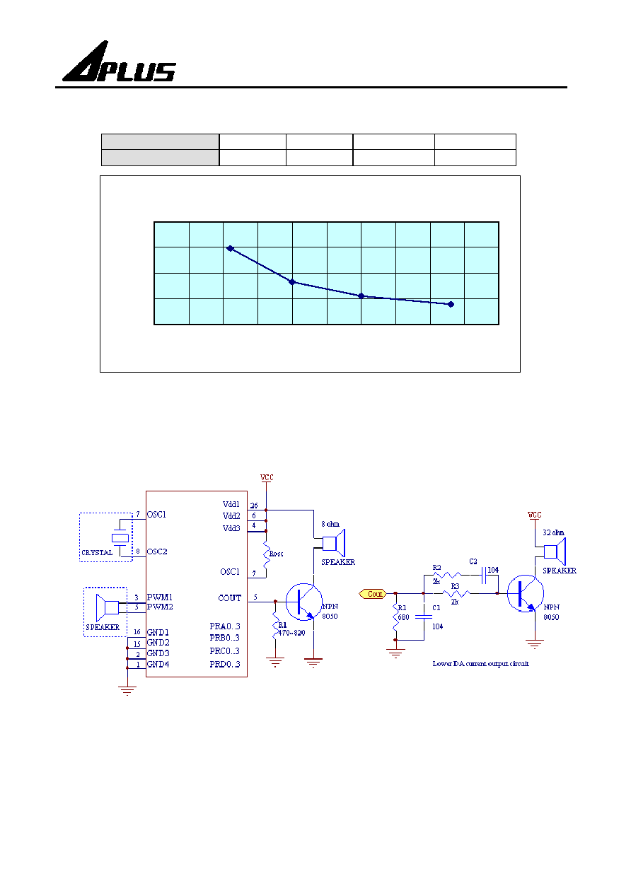
(10) Built-in 8 Level DAC current output can be configured. (Mask option)
(11) Built-in IR Carry Output: Port B[1] can be configured as IR pin by 38k / 56kHz. (Mask option)
(12) External Reset: Port B[3] can be configured as reset pin. (Mask opton)
(13) HALT and Release from HALT function to reduce power consumption
(14) Watch Dog Timer (WDT)
(15) Instruction: 1-cycle instruction except for table read and program branches which are 2-cycles
(16) Number of instruction: 27
(17) DAC: 1 channel voice and dual tone melody synthesizer (One 9-bits Cout or 8-bits PWM output).
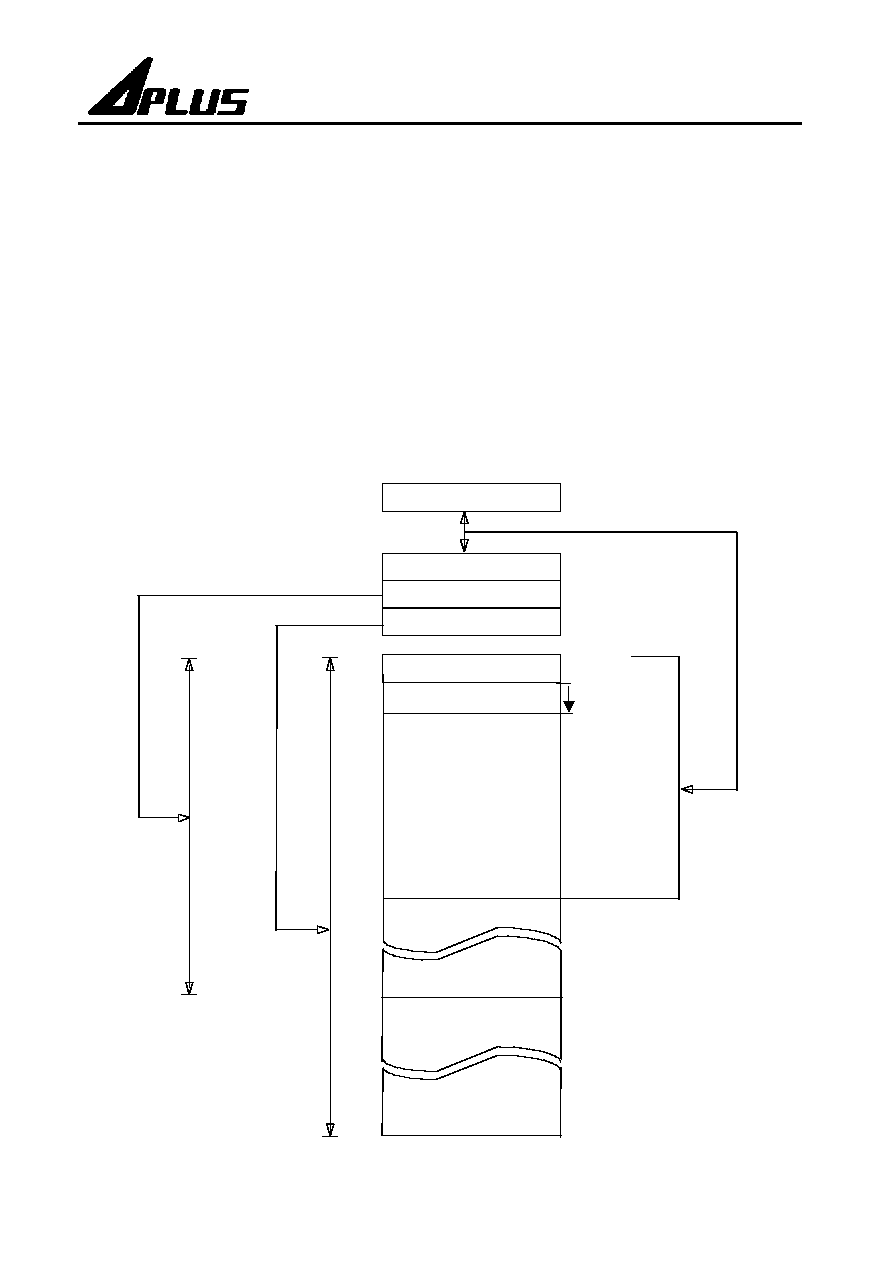
FIGURE 1 : ROM Map of
APExx16
Series
*
APE8416 /APE10616 /APE12716 are 64k x 10 bits
14-bit x 2 STACK
Reset Vector
00000h-03FFFh
16-bit Data Pointer
PC[13:0]
Reserved for Testing
000FFh-00400h
00401h
00000h
000FEh
Program ROM
00000h-0FFFFh
Data ROM for Melody
19-bit Voice Pointer
00000h-7FFFFh
Voice ROM for Voice
APExx16 Series
Rev 1.1 2003/9/2
3
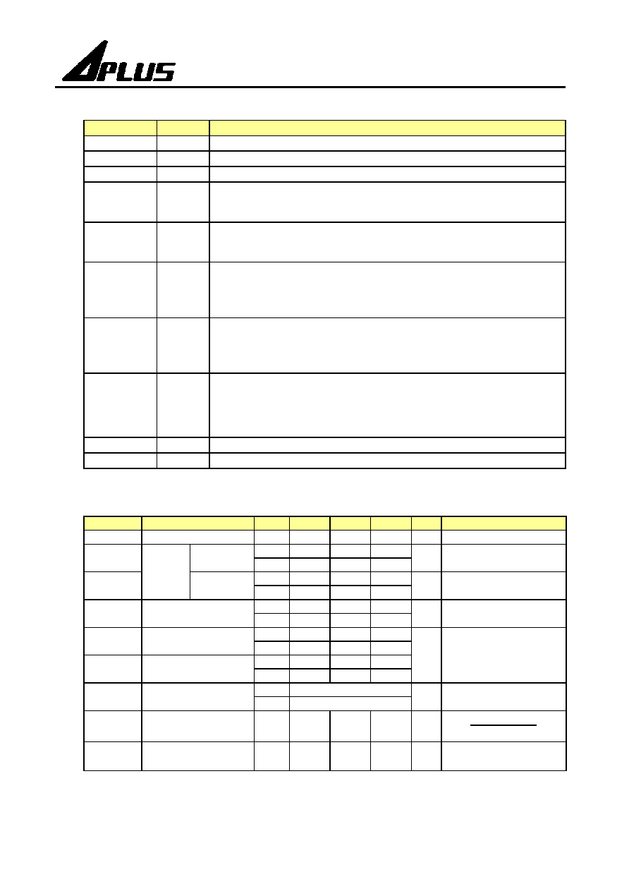
3.0 Pin Description
Pad Name
Pin Attr.
Description
PWM2/Cout
O
PWM2 output, or Current Output of Audio.
PWM1
O PWM1
output.
Vdd1~3
Power
Power supply during operation.
PRA0~3
PRC0~3
PRD0~3
I/O
I/O port can be programmed to input/output individually.
Input type with weak pull-low or fix-input-floating capability.
Buffer Output type.
PRB0 / OSC2
I/O
I/O port can be configured to input/output individually or HM OSC pad.
Input type with weak pull-low or fix-input-floating capability.
Buffer Output type.
PRB1 / IR
I/O
I/O port can be configured to input/output individually.
Input type with weak pull-low or fix-input-floating capability.
Buffer Output type.
Mask option selected as an IR Carrier Output with 38k / 56kHz
PRB2
I/O
I/O port can be configured to input/output individually.
Input type with weak pull-low or fix-input-floating capability.
Buffer Output type.
PRB3 / Reset
I/O
I/O port can be configured to input/output individually.
Input type with weak pull-low or fix-input-floating capability.
Buffer Output type.
Mask option selected as an external RESET pin with weak pull-low
capability.
OSC1
I
RM/HM mode Oscillator input
GND1~4
Power
Ground Potential
4.0 DC Characteristics
Symbol
Parameter
Vdd
Min.
Typ.
Max. Unit
Condition
Vdd
Operating voltage
2.4
3
5.5
V
depending on Freq.
3 1
Isb Standby
4.5 1
uA
4MHz, RM,
in HALT Mode
3 2
Iop
Supply
current
Operating
4.5 7
mA
4MHz, RM,
IO Floating
3 3
Iih
Input current
(Internal pull low)
4.5 10
uA
Input ports with weak
pull-low
3 -3
Ioh Output-high
current
4.5 -10
3 7
Iol Output-low
current
4.5 19
mA
4MHz, RM
(IO ports)
3
0.8 ~ 4.8
Cout
DAC output current
(8-level option)
4.5
0.9 ~ 6.5
mA
4MHz, RM
(Full scale)
dF/F Frequency
stability -5 5 %
Fosc(3v- 2.4v)
Fosc (3v)
dF/F
Fosc lot variation
-10
10
%
Vdd=3V, Rosc=180k,
4MHz