 | –≠–ª–µ–∫—Ç—Ä–æ–Ω–Ω—ã–π –∫–æ–º–ø–æ–Ω–µ–Ω—Ç: API8208A | –°–∫–∞—á–∞—Ç—å:  PDF PDF  ZIP ZIP |

Development tools support
∑
Low standby current (<5 µA at 3V)
∑
3.0V-6V single power supply operation
∑
Auto-power down
∑
rectly
2 drives buzzer or speaker di-
OUT
and V
1
OUT
∑ V
pin drives speaker with a transistor
OUT
∑ C
ptional pop noise elimination function
O
∑
quality
ADPCM data compression provides high sound
∑
Built-in D/A converter, EPROM
∑
ingle external resistor to determine sample rate
S
∑
Built-in oscillator with variable sample rate
∑
Pulse, BUSY Signal, and LED
Three programmable output pins for STP Stop
∑
RP interrupt pin for master reset
I
∑
15 ms debounce time suitable for CDS
∑
triggering option
Holdable and unholdable, edge and level
∑
SBT for sequential play-all or random play
∑
Four trigger pins, TG1 to TG4 for eight groups
∑
oice data re-use saves memory space
V
∑
extends the duration of playback
ombination of voice building blocks
C
∑
Versatile features for playback
∑
inimum 20 second voice length at 6 KHz
M
∑
FEATURES
trigger multiple groups playback in sequence.
controlled by TG1 toTG4 pins. The SBT pin can be used to
maximum of eight groups are available with activation
sections will form an individual group for data playback. A
subdivided into 126 sections. Any combination of these
The voice data memory area of the API8208A can be
Group of sections
of playback.
ramp-down function eliminates undesired noise at the end
filtering or amplifier circuit is needed. An automatic
speaker through a low cost NPN transistor. No complex
, enables the device to drive a
OUT
A current output pin, C
speaker.
2 provides direct drive to buzzer or
OUT
V
1 and
OUT
V
from 3.0V to 6.0V. PWM digital amplifier output pins,
The API8208A provides wide operating voltage range
background music each from one of two different chips.
external mixer in which speech can be mixed with
parallel in order to achieve signal mixing without an
longer voice duration. Two devices can be configured in
duration. In addition, devices can be cascaded to achieve
Versatile combinations in sections achieve longer playback
sounds and even special sound effects can be synthesized.
Sounds such as human speech, animal sounds, musical
in voice playback but still achieves high voice quality.
The API8208A eliminates the need of complicated circuitry
voice data at 6 KHz sample rate.
on-chip EPROM which can store up to 20 seconds of
is used. The audio message is stored in a 512K bits
varying playback duration. A proprietary ADPCM algorithm
API8208A is a high quality voice synthesizer capable of
GENERAL DESCRIPTION
VOICE ROM
ANT
TILE 20 SEC INST
VERSA
11/15/99
1
APLUS API8208A

2
APLUS API8208A
Group Configuration
Voice within each group are combinations of different
fixed memory sections of up to 126 sections. These
sections are the fundamental voice building blocks for
arranging playback without limiting sequencing. This
provides flexibility and allows data to be re-used, beneficial
for applications with many repeated sounds or words.
An example of group configuration is illustrated below:
Group No.
Section Entry
Group 1
Sec 1 + Sec 2 + Sec 3 ....... Sec 109
Group 2
Sec 3 + Sec 2
Group 3
Sec 10 + Sec 11 + Sec 12
Group 4
Sec110 + Sec 10 + Sec 5
Group Configuration
The entry of sections for each group is truly random and
without limitation. However, there is a limit in the total
number of entries for eight groups, which is 992 in the
API8208A It is acceptable to allocate all entries into only
one group or distribute out to other groups. It depends on
how many groups of messages are required.
Programmable Options
Groups in API8208A can have independent options. They
include:
∑
Edge or Level trigger
∑
Unholdable or Holdable trigger
∑
Retriggerable or non-retriggerable
∑
Sequential or Random playback
∑
LED1, LED2, Busy, and Stop pulse are configurable
∑
Four selections in playback frequency
Selections in Triggering
The API8208A can be triggered in different ways, Edge or
Level trigger, Holdable or Unholdable, Retriggerable or
Non-retriggerable. The combinations of the triggering
options provide versatile playback.
By enabling Retrigger, the playback can be controlled in
Stop and Start mode. A trigger on any trigger pin will stop
the current message and start the next message immedi-
ately.
Selections in Playback Frequency
This option provides four choices for each group in
frequency which implies it is possible to have four
different sampling rates in one chip or one sample rate
with a different playback frequency. As a matter of fact,
the available choices are also dependent on the pullup
resistor value at the OSC pin. For example, if the
fundamental frequency choice is F, it can provide choices
in x1, x1-1/2, x2, x3.
Selections in Playback Mode
There are two playback modes, Sequential and Random
in the API8208A If the chip is programmed in Sequential
Mode, messages will playback in the order from Group 1
to Group 8 by triggering the SBT pin. If the chip is
programmed in Random Mode, messages will be played
back randomly by triggering the SBT pin.
Selections in Output Buffer
There are three independent output pins, OUT1, OUT2,
and OUT3, available for several combinations of LED1,
LED2, Stop Pulse, and Busy Signal for each group. The
following table illustrates the four different combinations.
OUT1 OUT2 OUT3
1. LED1 Busy LED2
2. Stop LED2 LED1
3. Busy LED1 Stop
4. LED2 Stop Busy
LED1 and LED2 are complemented outputs flashing at
approximately a 3 Hz rate. Stop pulse (STOP) gives a 15
ms positive pulse at the end of the playback for each
Group with option have or do not have the Stop pulse.
Busy is active high and Section dependent but not Group
dependent. Even if same section in different group may
have different output in Busy output. For instance, BUSY
can be high for Section 4 in Group 1 but low in Group 4.
BUSY can be used as a synchronous signal. During
standby mode all three outputs must be low.
Software Support
APLUS provides dedicated software to the customer. With
this tool, the customer can compose their own messages
and configure the chip to fit into their applications very
easily.
3
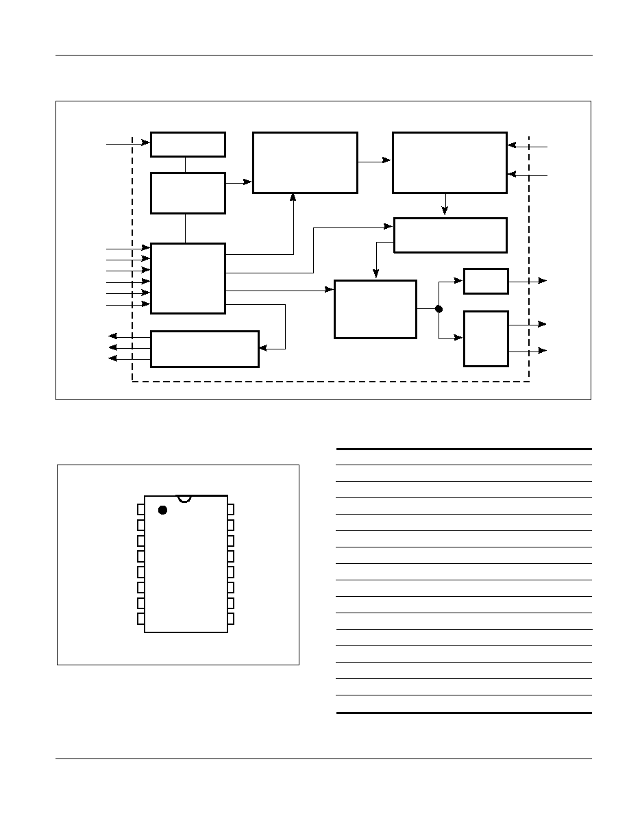
OSCILLATOR
OSC
CLOCK
GENERATOR
CONTROL
LOGIC
TG1
TG2
TG3
TG4
SBT
IRP
OUTPUT
DRIVER
OUT1
OUT2
OUT3
POP NOISE
REDUCTION
ADDRESS
SEQUENCER
VOICE
EPROM
ADPCM
DECODER
BUZZER
BUFFER
D/A
C
OUT
V
OUT1
V
OUT2
GND
V
CC
BLOCK DIAGRAM
PIN DESCRIPTION
OUT1
Programmable output 1
OUT2
Programmable output 2
OUT3
Programmable output 3
V
OUT
1
PWM audio signal output for buzzer and speaker
V
OUT
2
PWM audio signal output for buzzer and speaker
GND
Power ground
C
OUT
Current output from internal DAC for speaker playback
OSC
Oscillator resistor pin to control sampling frequency
V
PP
Program power supply, no connect when voice playback
TG1
Trigger switch 1, internal pull low, active high
Trigger switch 2, internal pull low, active high
V
CC
Positive power supply
TG3
Trigger switch 3, internal pull low, active high
TG4
Trigger switch 4, internal pull low, active high
SBT
Sequential trigger, internal pull low, active high
IRP
Interrupt to stop playback, internal pull low, active high
Note:
1. The following pins are used to program data into the memory:
pins 4, 5, 6, 8, 9, 12, 15 and 16.
PIN CONFIGURATIONS
300-mil PDIP
1
2
3
4
5
6
7
8
16
15
14
13
12
11
10
9
OUT1
V
OUT1
V
OUT2
GND
OUT2
OUT3
C
OUT
OSC
IRP
SBT
TG4
TG3
V
CC
TG2
TG1
V
PP
APLUS API8208A
TG2
4
ABSOLUTE MAXIMUM RATINGS
Symbol
Parameter
Value
Unit
V
CC
- GND
Terminal Voltage with Respect to GND
≠0.5 to +7.0
V
V
IN
GND ≠ 0.3 < V
IN
< V
CC
+ 0.3
V
V
OUT
GND < V
OUT
< V
CC
V
T
A
Operating Temperature
≠10 to +85
∞C
T
STG
Storage Temperature
≠55 to +125
∞C
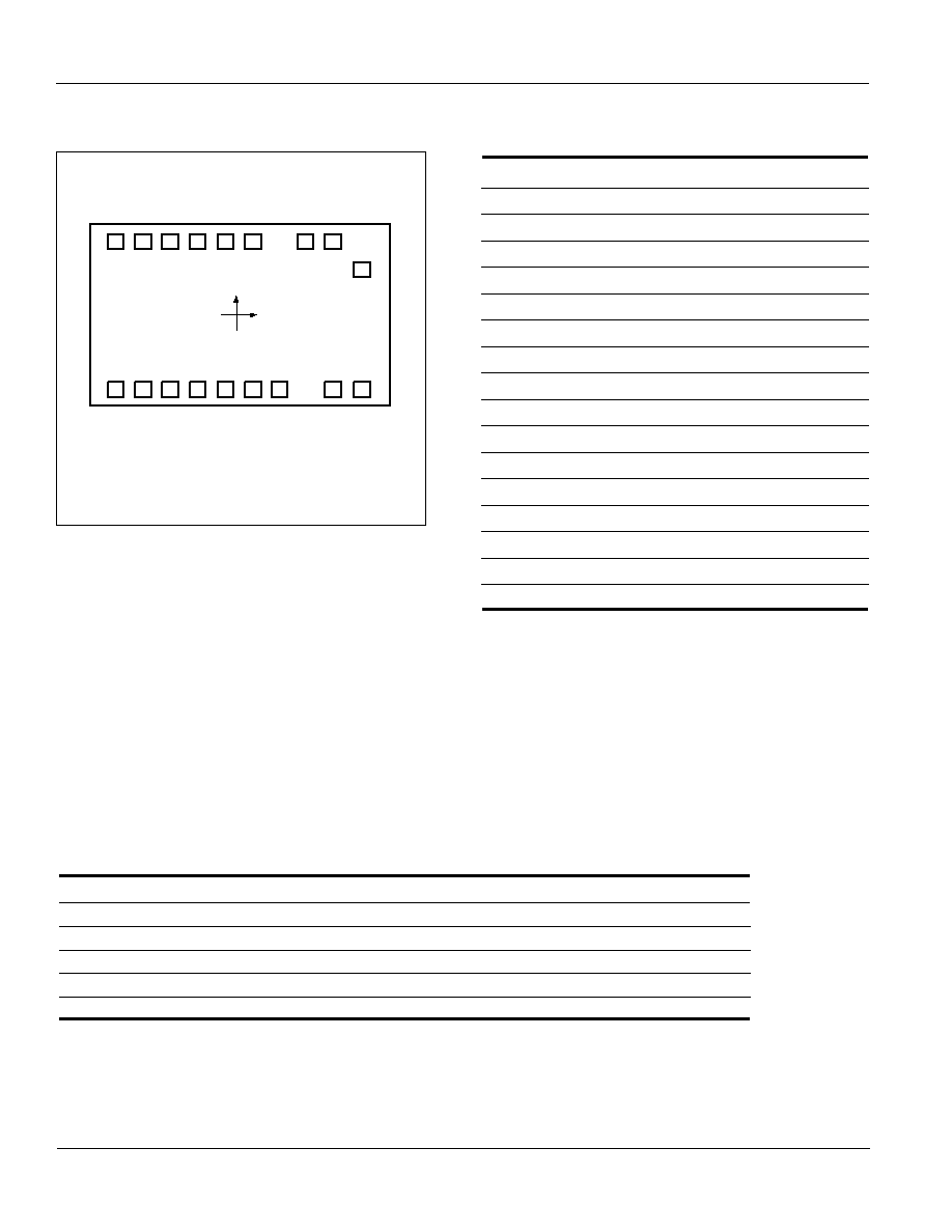
BONDING PARAMETERS
Pin
Name
X
Y
1
OUT1
-6
≠1017
2
V
OUT1
297
≠1017
3
V
OUT2
803
≠1017
4
GND
1058
≠1017
5
OUT2
927
1017
6
OUT3
697
1017
7
C
OUT
199
1017
8
OSC
≠103
1017
9
V
PP
≠358
1017
10
TG1
≠566
1017
11
TG2
≠810
1017
12
V
CC
≠1059
1017
13
TG3
≠934
≠1017
14
TG4
≠689
≠1017
15
SBT
≠444
≠1017
16
IRP
≠200
≠1017
BONDING DIAGRAM
Note:
Programming requires connection to
pins 4, 5, 6, 8, 9, 12, 15, and 16.
12
11
10
9
8
7
6
5
13
14
15
16
2
4
1
3
NC
NC
(0,0)
X
Y
Note: Substrate must be connected to GND
Pad size = 80 µm x 80 µm
Die size = 2350 x 2260 µm
92.5 x 88.97 mil
APLUS API8208A

5
DC CHARACTERISTICS
Symbol
Parameter Description
Test Conditions
Min.
Typ.
Max.
Unit
V
CC
Operating Voltage 3.0 4.5 5.0 V
I
SB
Standby Current
Vcc = 3.0V, I/O Open
--
1
5
µA
I
OP
Operating Current
Vcc = 3.0V, I/O Open
--
--
100
µA
V
IH
Input HIGH Voltage
Vcc = 3.0V
2.5
3.0
3.5
V
V
IL
Input LOW Voltage
Vcc = 2.0V
≠0.3
0
0.3
V
I
OH
V
OUT
HIGH Operating Current
Vcc = 3.0V, V
OUT
= 3.0V
--
≠12
--
mA
I
OL
V
OUT
LOW Operating Current
Vcc = 3.0V, V
OUT
= 0V
--
12
--
mA
I
CO
C
OUT
Operating Current
Vcc = 3.0V, V
COUT
= 0.7V
--
≠2
--
mA
I
STPH
STP HIGH Operating Current
Vcc = 3.0V, V
STP
= 3.0V
--
≠5
--
mA
I
STPL
STP LOW Operating Current
Vcc = 3.0V, V
STP
= 0V
--
5
--
mA
I
LED
LED Output Current
Vcc = 2.2V ≠ 6.0V
6
8
10
mA
–F/F
Frequency Stability
(F
OSC
[3V] ≠ F
OSC
[3.5V]) / F
OSC
(3.0V)
--
--
5
%
SAMPLING FREQUENCY vs
R
OSC
FOR API8208A
Common Sampling Rate vs. Oscillator Resistor
Sampling Frequency
R
OSC
KHz Kohm
5.0 290
5.5 262
6.0 240
6.5 220
7.0 201
7.5 187
8.0 174
8.5 162
9.0 153
9.5 143
10.0 135
10.5 127
11.0 120
12.0 108
SAMPLING FREQUENCY vs
R
OSC
FOR API8208A
Common Resistors vs. Sampling Rate
Sampling Frequency Rosc
KHz KOhm
13.0 100
14.0 91
16.0 82
22.0 54
APLUS API8208A