PIN DESCRIPTIONS
Pin NO.
I/O
Symbol
Function
1
I
P1.2/OEB/Mode option
Bit 2 of Port 1 / Program control signal
2
I
P1.1/PGMB/Mode option
Bit 1 of Port 1 / Program control signal
3
I
P1.0
Bit 0 of Port 1
4
I
VSS
Negative power supply.
5
I
OSC/ACLK
Oscillation component connection pin /
Program control signal
6
I
TEST/Vpp
Test/Programing.
7
O
VO2
Voice output.
8
VO1
No connect
9
I
VDD
Positive power supply.
10
I/O
P3.3
Bit 3 of Port 3.
11
I/O
P3.2
Bit 2 of Port 3.
12
I/O
P3.1
Bit 1 of Port 3.
13
I/O
P3.0
Bit 0 of Port 3.
14
I/O
P2.3
Bit 3 of Port 2.
15
I/O
P2.2
Bit 2 of Port 2.
16
I/O
P2.1/Dout
Bit 1 of Port 2 / Program data output signal
17
I/O
P2.0/Din
Bit 0 of Port 2 / Program data input signal
18
I/O
P1.3/Din.out.clk/Mode option
Bit 3 of Port 1 / Program control signal
GENERAL DESCRIPTION
API820G is a tiny-controller-based voice synthesizer IC which contains all the function of API820G series
and has an OTP (One Time Programmable) ROM inside.
FEATURES
� API820G � ROM : 64k x 10 bits (21 sec@6K sample rate).
� Single power supply 2.4V ~ 5.5V.
� Port1 and Port2 with wake-up function.
� Power down mode for saving power consumption.
� Single ROM for voice and program data.
� Readable ROM code data.
� One 6-bit timer overflow control.
� Two stacks for subroutine calling.
� Fixed current D/A to drive external connected transistor for audio output.
� 5-bit ASPCM synthesizer.
� Multiple levels of volume control.
� Multiple playing sppeeds in 2KHz ~ 32KHz for voice playback.
1
API 820G
� Multiple playing sppeeds in 2KHz ~ 32KHz for voice playback.
2
TIMING PARAMETER
Symbol
Parameter
Min.
Max.
Unit
Trs
Level set up time
2
us
Tmcs
Mode code setup time
2
us
Tdsu
Data set up time
100
ns
Tdsh
Data hold time
100
ns
Tas
ACLK to byte select time
2
us
Tacpw
Address clock pulse width
2
us
Tppw
Program pulse width
100
us
Tps
Programming mode set up time
4
us
Toed
Output enable setup time
300
ns
Note : Segment ROM S1, S0 is programed just while 5 LSBs of ADDR are all 0.
Programming for security mode :
When programming in security mode, the waveform is just like above. The programming data is as below :
B11 ~ B1
B0
User defined
Security bit
Note : When security = 0, enable security;
When security = 1, disable security.
PROGRAMMING MODE
Mode
P13
P12
P11
Regular
0
0
0
Security
0
0
1
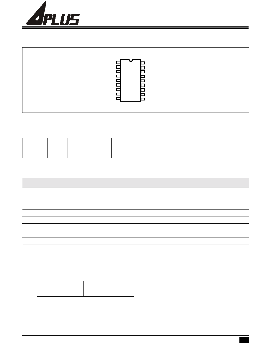
PIN ASSIGNMENT
API 820G
18 pin DIP
1
2
3
4
5
6
7
8
9
18
17
16
15
14
13
12
11
10
P1.2
P1.1
P1.0
GND
OSC
VPP
VO2
VO1
VDD
P1.3
P2.0
P2.1
P2.2
P2.3
P3.0
P3.1
P3.2
P3.3
API 820G
DC PROGRAMMING CHARACTERISTICS
(
V
DD
= 5V+0.5v, V
PP
= 12.5V+0.5v)
Items
Sym.
Min.
Max.
Unit
Test Conditions
Input high voltage
V
IH
2.2
V
DD
+1.0
V
Input low voltage
V
IL
-0.3
0.8
V
Input current
I
IN
-
10
�A
V
DD
=5V, V
IN
=0~V
DD
Output high voltage
V
OH
2.4
-
V
I
OH
=400�A
Output low volatge
V
OL
-
0.4
V
I
OL
=2.1mA
VDD supply current
I
DD
-
100
mA
V
DD
=5V
VPP supply current
I
PP
-
50
mA
V
PP
=12.5V
ELECTRICAL CHARACTERISTICS
(
V
DD
= 3V,25
o
C unless otherwise specified)
Parameter
Sym.
Min.
Typ.
Max.
Unit
Condition
Operating voltage
V
DD
2.4
3.0
5.5
V
Standby current
I
DDS
-
-
1.0
�A
V
DD
=3V
Operating current
I
DDO
-
-
250
�A
V
DD
=3V, No load
Drive current of P2,P3
I
OD
2.0
3.0
-
mA
V
DD
=3V, V
O
=2.4V
Sink current of P3
I
OS
2.3
3.5
-
mA
V
DD
=3V, V
O
=0.4V
Sink current of P2 (after KEYB)
I
OS1
2.3
3.5
-
mA
V
DD
=3V, V
O
=0.4V
Sink current of P2
I
OS2
-
3.0
10
�A
V
DD
=3V, V
O
=0.4V
(before KEYB)
Input current of P1
I
IH
-
3.0
10
�A
V
DD
=3V
Output current of VO1, VO2
I
VO
4.0
5.0
6.0
mA
V
DD
=3V, V
O
=0.7V,
two channel full scale output
Oscillation resistor
Rosc
-
100
-
K
V
DD
=2.4V ~ 5.5V
Oscillator frequency
F
osc
0.9
1.0
1.1
MHz
V
DD
=2.4V ~ 5.5V
Oscillator frequency deviation
F
osc
/
F
osc
-10
-
10
%
V
DD
=2.4V ~ 5.5V
ABSOLUTE MAXIMUM RATINGS
Items
Sym.
Min.
Max.
Unit
Supply Voltage
V
DD
-V
SS
-0.3
6.0
V
Input Voltage
V
IN
V
SS
-0.3
V
DD
+0.3
V
Operating Temperature
T
O P
0
70
o
C
Storage Temperature
T
STG
-55
+125
o
C
3
API 820G
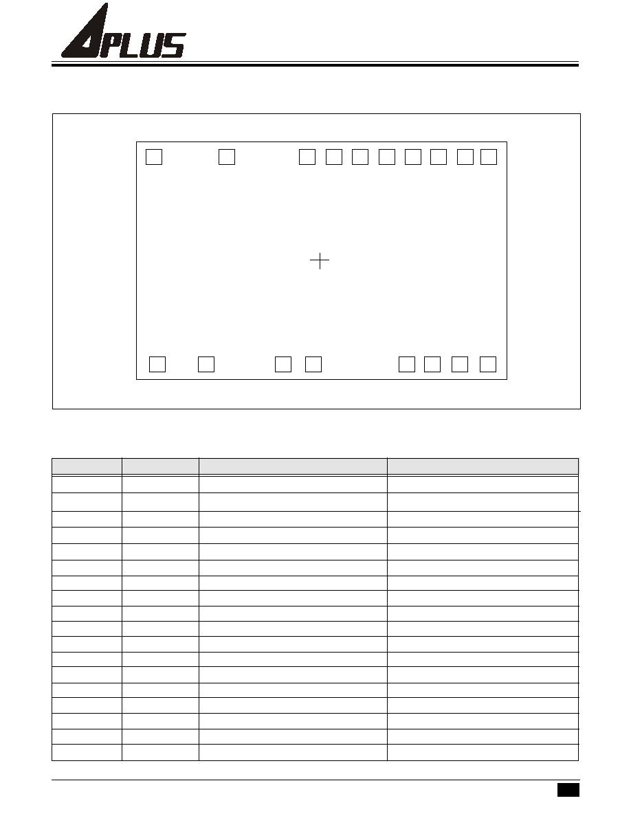
4
Pad No.
Symbol
X
Y
1
P1.2
325.8
900.6
2
P1.1
128.7
900.6
3
P1.0
-56.5
900.6
4
GND
-708.4
876.7
5
OSC
-1325.0
879.0
6
VPP
-1256.2
-890.0
7
VO2
-879.3
-890.0
8
VO1
-233.4
-890.0
9
VDD
-13.7
-878.4
10
P3.3
963.2
-878.4
11
P3.2
1084.1
-878.4
12
P3.1
1205.0
-878.4
13
P3.0
1325.9
-878.4
14
P2.3
1275.9
900.6
15
P2.2
1090.6
900.6
16
P2.1
893.5
900.6
17
P2.0
708.2
900.6
18
P1.3
511.1
900.6
PAD DIAGRAM
Chip Size : 2930 x 2100 um
For PCB layout, IC substrate must be connected to Vss.
(0,0)
API 820G
9
6
3
2
1
18
17
16
15
14
7
8
10
11
12
13
P3.0
P1.1
P2.3
P2.2
P3.1
P2.1
P2.0
P1.3
P1.2
P1.0
VPP
VDD
VO1
GND
OSC
4
5
P3.2
P3.3
VO2
API 820G
VO1
P2.2
P3.3
P3.2
P2.1
P2.0
P3.0
P3.1
VDD
VSS
TEST
OSC
P2.3
P1.0
P1.1
P1.2
P1.3
VO2
470k
�
�
�
*"5.!!
VO1
P2.2
P3.3
P3.2
P2.1
P2.0
P3.0
P3.1
VDD
VSS
TEST
OSC
P2.3
P1.0
P1.1
P1.2
P1.3
VO2
470k
�
�
5
* This specification are subject to be changed without notice.
API 820G
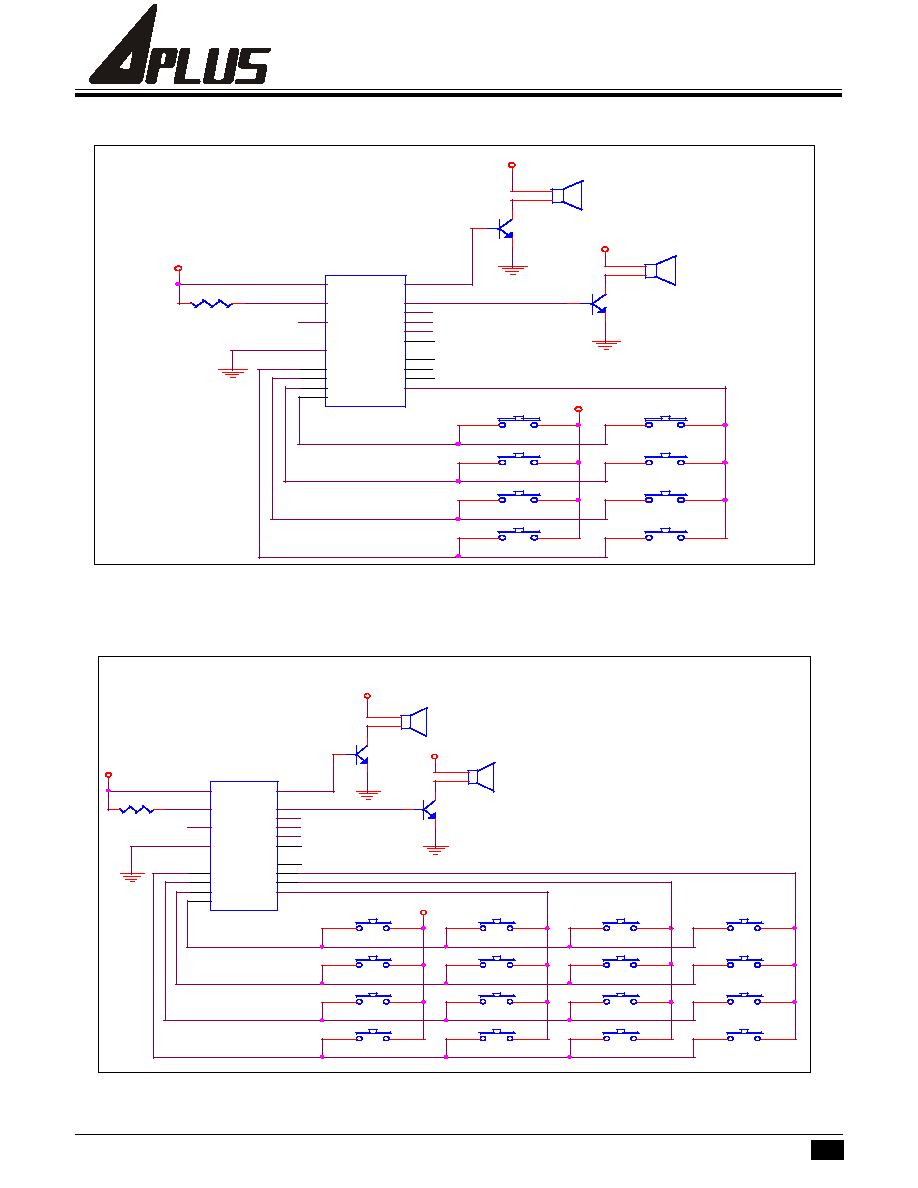
16 Key Application Circuit
8 Key Application Circuit