6F-3 NO.7, LANE 75, TA-AN ROAD, SEC.1, TAIPEI, TAIWAN, R.O.C.
http://www.aplusinc.com.tw
7576F-3 TEL:886-2-27818277 FAX:886-2-27815779
ASM0406CB/0906CB
DATA SHEET

Rev 1.0
1
ASM0406CB/0906CB
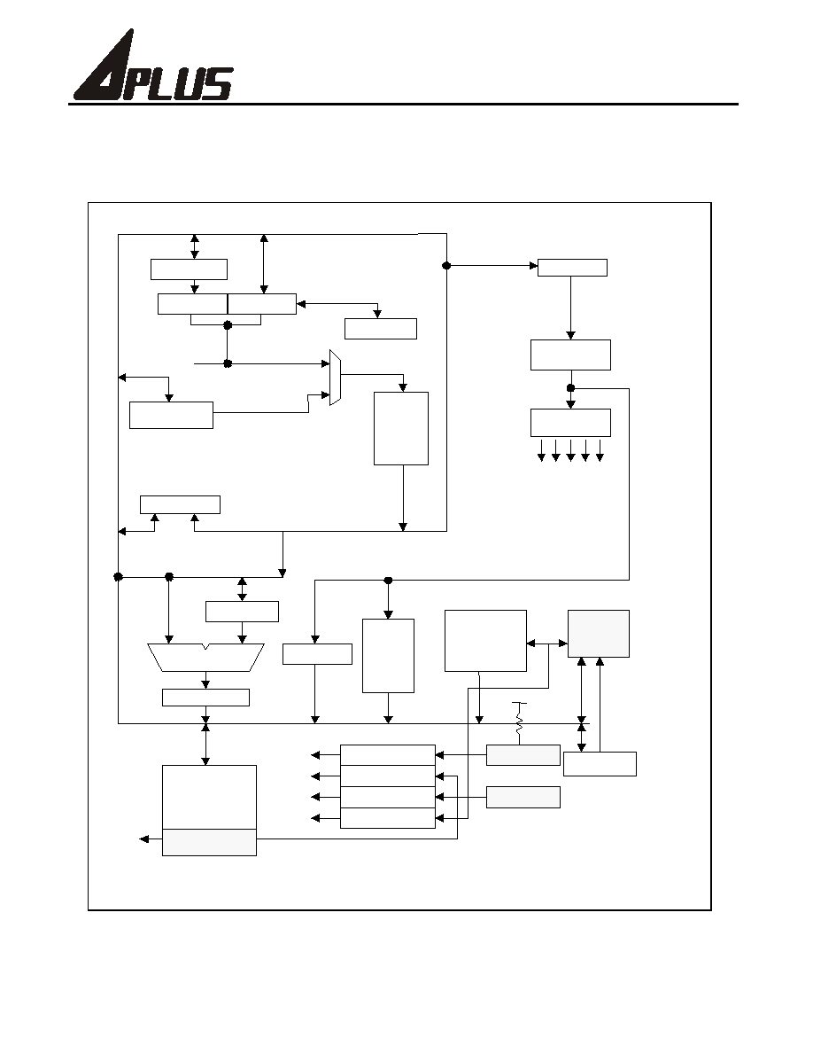
1.0 General Description
The
ASM0406CB/0906CB is very low cost voice synthesizer with 4-bit microprocessor. It has
various features including 4-bit ALU, ROM, RAM, I/O ports, timers, clock generator,
watchdog timer ( WDT ), voice synthesizer, etc. It consists of 22 instructions in the device.
With CMOS technology and halt function can minimize power dissipation. Its architecture is similar
to RISC,with two stages of instruction pipeline. It allows all instructions to be executed in a single
cycle, except for program branches and data table read instructions (which need two
instruction cycles).
1.1 Feature
Single power supply can operate from 2.4V through 5.5V
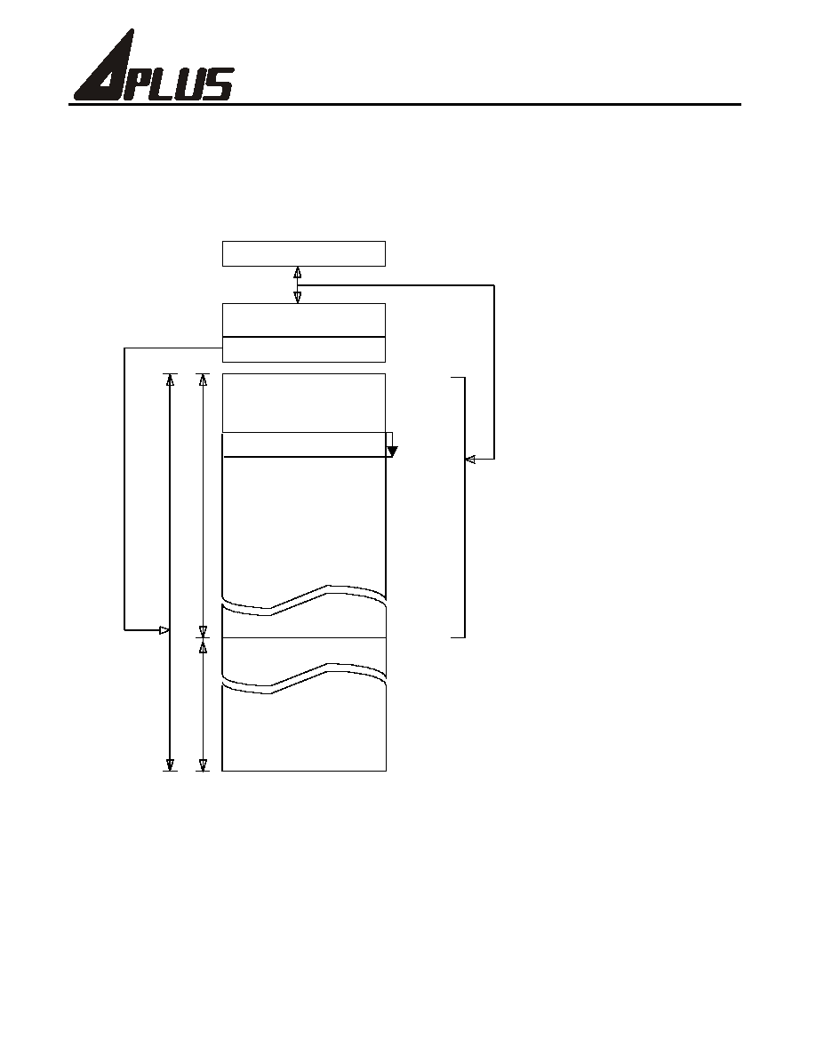
Internal Program ROM: 4K x 10-bit
1 sets of 15-bit DPR can access up to 32K x 10 bits data memory space
Data Registers:
� 64 x 4-bit data RAM (00-1Fh plus 40h-5Fh)
� Unbanked special function registers (SFR) range: 20h-3Fh
I/O Ports:
� PRA: 4-bit I/O Port A (2Bh)
� PRB: 2-bit Output Port B (2Dh)
On-chip clock generator:
Resistive Clock Drive(RM)
Timer: 1
� Timer0: a 9-bit auto-reload timer/counter
Stack: 2-level subroutine nesting
HALT and Release from HALT function to reduce power consumption
Watch Dog Timer (WDT)
Instruction: 1-cycle instruction except for table read and program branches which are 2-cycles
Number of instruction: 22
The Voice function can be implemented by microprocessor instruction
� One 8-bit COUT output for ASM0406CB/0906CB
ASM0406CB/0906CB
- VERY LOW-COST VOICE SYNTHESIZER WITH 4-BIT MICROPROCESSOR

Rev 1.0
4
1.2 Pin-Out
ASM0406CB/0906CB Pin-Out
VDD
I
-
Power supply during operation
PRA3-1
I/O
STI
Std./O.D.
I/O port with programmable strong pull-low or weak pull-low or fix-input-
floating capability
Output type with standard or Open-Drain output
PRA0/RESET I/O
STI
Std./O.D.
I/O port with programmable strong pull-low or weak pull-low or fix-input-
floating capability
Output type with standard or Open-Drain output
Mask option selected as an external RESET pin with weak pull-low capability
OSC
I
-
RM mode Oscillator input
COUT
O
-
Current Output of Audio
GND
I
-
Circuit Ground Potential
TEST
O
-
Enter Test Mode. ( TEST = High )
PRB0-1
O
Std./O.D. Output type with standard or Open-Drain output
1.3 Application circuit
ASM0406CB/0906CB