 | –≠–ª–µ–∫—Ç—Ä–æ–Ω–Ω—ã–π –∫–æ–º–ø–æ–Ω–µ–Ω—Ç: ASM4112C | –°–∫–∞—á–∞—Ç—å:  PDF PDF  ZIP ZIP |

6F-3 NO.7, LANE 75, TA-AN ROAD, SEC.1, TAIPEI, TAIWAN, R.O.C.
http://www.aplusinc.com.tw
7576F-3 TEL:886-2-27818277 FAX:886-2-27815779
ASM3112C/4112C
DATA SHEET

Rev 1.0
1
ASM3112C/4112C ≠
VERY LOW-COST VOICE SYNTHESIZER WITH 4-BIT MICROPROCESSOR
1.0 General Description
The ASM3112C/4112C is very low cost voice synthesizer with 4-bit microprocessor. It has various
features including 4-bit ALU, ROM, RAM, I/O ports, timers, clock generator, watchdog timer(WDT),
voice synthesizer, etc. It consists of 22 instructions in the device. With CMOS technology and halt
function can minimize power dissipation. Its architecture is similar to RISC, with two stages of
instruction pipeline. It allows all instructions to be executed in a single cycle, except for program
branches and data table read instructions (which need two instruction cycles).
1.1 Feature
Single power supply can operate from 2.4V through 5.5V
Internal Program ROM: 4K x 10-bit
1 sets of 17-bit DPR can access up to 128K x 10 bits data memory space
Data Registers:
∑ 96 x 4-bit data RAM (00-1Fh plus 40h-7Fh)
∑ Unbanked special function registers (SFR) range: 20h-3Fh
I/O Ports:
∑ PRA: 4-bit I/O Port A (2Bh)
∑ PRB: 4-bit Output Port B (2Dh)
∑ PRC: 4-bit Input Port C (2Fh)
On-chip clock generator: Resistive Clock Drive(RM)
Timer: 1
∑ Timer0: a 9-bit auto-reload timer/counter
Stack: 2-level subroutine nesting
HALT and Release from HALT function to reduce power consumption
Watch Dog Timer (WDT)
Instruction: 1-cycle instruction except for table read and program branches which are 2-cycles
Number of instruction: 22
The Voice function can be implemented by microprocessor instruction
∑ One 8-bit COUT output for ASM3112C/4112C
ASM3112C/4112C

Rev 1.0
2
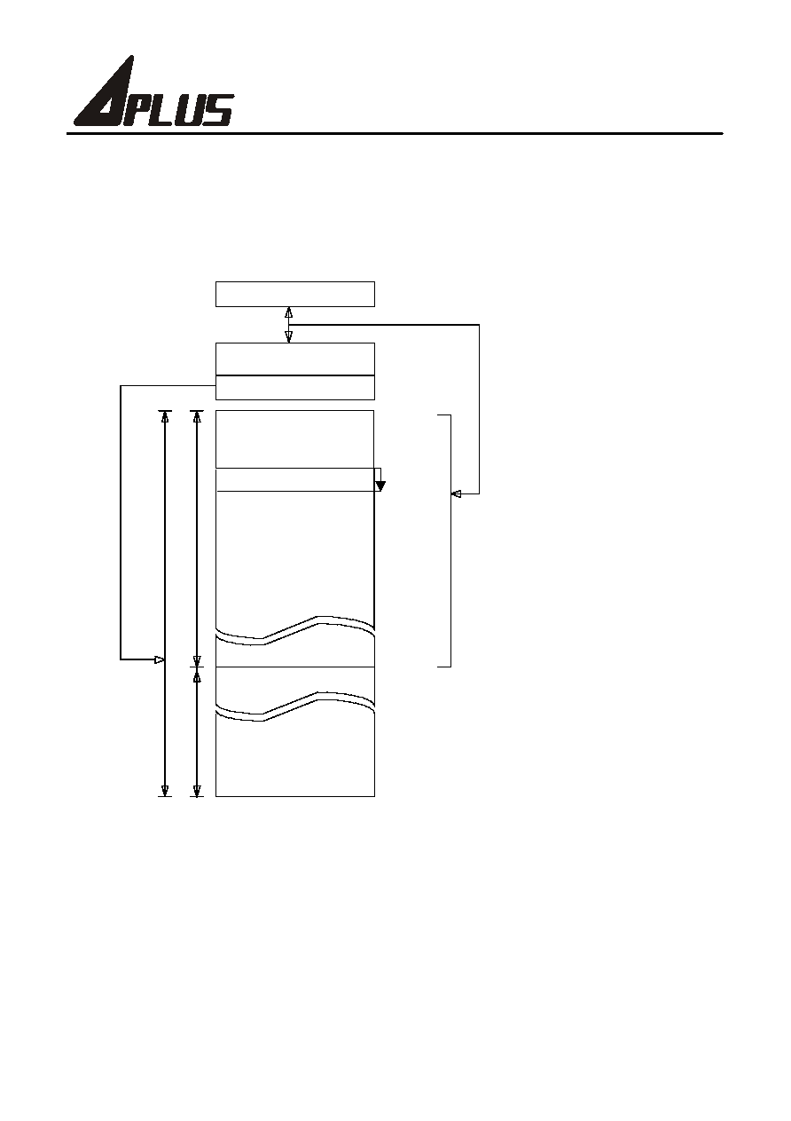
FIGURE 1.1 : Block Diagram of ASM3112C/4112C
COUT
OSC
VDD/GND
ROM
1
PC[11:0]
ROM Latch
Instruction
Latch
Instruction
Decoder
0
PCH(8)
PCL(4)
PCLATCH(8)
DPR3,2,1
Program
DLATCH(10)
Clock Generator
Power on Reset
Test select
P1,P2,P3,P4
enter test mode
Timer0(9)
Reset Chip
Stack(12)
Data Bus[3:0]
Instruction Bus [9:0]
ROM_ADDR[16:0]
ROM_Data[9:0]
Data Bus[3:0]
Control Signal
ADDR[16:0]
=0000b
(ADDR[16:12])
PRASL(4)
weak or strong
pull-low for PRA,
(Data)
In
s
t
ru
cti
o
n
Bu
s
[
9
:
0
]
Instruction Bus [9:0]
( Voice synthesizer )
One-Channel
SRAM
(96 x 4)
40h-7Fh
(2-Level)
ALU(4)
Register(4)
Accumlator(4)
Immediate(4)
DPR[16:0]
RESET pin
Reset Chip
PR
A
0
00h-1Fh
PRA(4)
PRB(4)
PRC(4)
PRB, PRC
COUT
ASM3112C/4112C
Rev 1.0
3
FIGURE 1.2 : External ROM Map of ASM3112C/4112C
Da
ta RO
M
12bit x 2 STACK
Reset Vector
1FFFFh(128Kx10-bits)
00FFFh(4K)
00000h-00FFFh
Pro
g
ram
and
data
ROM
17-bit Data Pointer
PC[11:0]
00000h-1FFFFh
Reserved for Testing
00080h-003FFh
00400h
00000h
00080h
ASM3112C/4112C
Rev 1.0
4
1.2 Pin-Out
ASM3112C/4112C Pin-Out
PRC1
I
STI
Std./O.D.
Input port with programmable strong pull-low or weak pull-low or
fix-input-floating capability
PRC0/RESET
I
STI
Std./O.D.
Input port with programmable strong pull-low or weak pull-low or
fix-input-floating capability
Mask option selected as an external RESET pin with weak pull-low capability
PRA3-1
I/O
STI
Std./O.D.
I/O port with programmable strong pull-low or weak pull-low or
fix-input-floating capability
Output type with standard or Open-Drain output
PRA0/RESET
I/O
STI
Std./O.D.
I/O port with programmable strong pull-low or weak pull-low or
fix-input-floating capability
Output type with standard or Open-Drain output
Mask option selected as an external RESET pin with weak pull-low capability
OSC
I
-
RM mode Oscillator input
VDD1
I
-
First Power supply during operation
COUT
O
-
Current Output of Audio
GND1
I
-
First Circuit Ground Potential
GND2
I
-
Second Circuit Ground Potential
TEST
O
-
Enter Test Mode. ( TEST = High )
VDD2
I
-
Second Power supply during operation
PRB0-3
O
Std./O.D.
Output type with standard or Open-Drain output
PRC2-3
I
STI
Std./O.D.
Input port with programmable strong pull-low or weak pull-low or
fix-input-floating capability
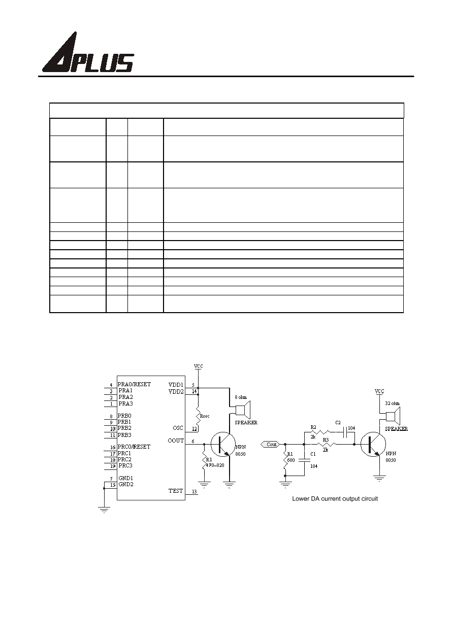
1.3 Application circuit
ASM3112C/4112C

Rev 1.0
5
1.4 Bonding Diagram
Substrate must be connected to GND.
ASM3112C/4112C Pad Location Chip Size: X=1540+100 (um), Y=2320+100 (um)
PAD # PAD Name
X
Y
PAD # PAD Name
X
Y
1 RA3
-682.16
-1040.2 11 RB3
667.68
-1040.2
2 RA2
-559.84
-1040.2 12 OSC
633.56
1071.52
3 RA1
-437.52
-1040.2 13 TEST
432.48
1071.52
4 RA0
-315.2
-1040.2 14 VDD2
273.16
1071.52
5 VDD1
-191.28
-1040.2 15 GND2
134.68
1071.52
6 COUT
71.12
-1040.2 16 RC0
-51.76
1071.52
7 GND1
189.52
-1040.2 17 RC1
-248.4
1071.52
8 RB0
307.92
-1040.2 18 RC2
-454.24
1071.52
9 RB1
430.24
-1040.2 19 RC3
-650.88
1071.52
10 RB2
552.56
-1040.2
19 18 17 16 15 14 13 12
RC3 RC2 RC1 RC0 GND2 VDD2 TEST OSC
ASM3112C/4112C
RA3 RA2 RA1 RA0 VDD1 COUT GND1 RB0 RB1 RB2 RB3
1 2 3 4 5 6 7 8 9 10 11
( 128K x 10-bit ) Block ROM
ASM3112C/4112C

Rev 1.0
6
1.5 DC Characteristics for ASM3112C/4112C
SYMBOL PARAMETER VDD
MIN.
TYP.
MAX.
UNIT
CONDITION
VDD
OPERATING
VOLTAGE
2.4 3 5.5 V
depending
on
Freq.
3 1
Isb
STANDBY
5 1
uA
4MHz, RM
in HALT Mode
3 2
Iop
SUPPLY
CURRENT
OPERATING
5 7
mA
4MHz, RM
IO Floating
3 3
5 9
Iih
INPUT CURRENT
/Internal pull low
5
-5.2
uA
4MHz, RM
in HALT Mode
(IO Ports with
weak pull-high
pull-low)
3 -3
Ioh
OUTPUT HIGH
CURRENT
5 -8
3 7
Iol
OUTPUT LOW
CURRENT
5 20
mA
4MHz, RM
(IO ports)
dF/F
FREQUENCY
STABILITY
-10 10 %
Fosc(3v- 2.4v)
Fosc (3v)
dF/F Fosc
VARIATION
-20
20
%
VDD=3V,
Rosc=180k, 4MHz
FIGURE 1.3 : Frequency Range for Rosc in RM mode
Resistor(k ohm)
300
220
180
150
3v Freq.(MHz)
2.54 3.54 3.99 5.49
R osc & Freq.
2.54
3.54
3.99
5.49
0
1
2
3
4
5
6
0
100
200
300
400
R osc k ohm
Freq. MHz
ASM3112C/4112C