Document Outline
- ARM1026EJ-S
- Change history
- Contents
- List of Tables
- List of Figures
- Preface
- Introduction
- Integer Core
- Programmerês Model
- Clocking and Reset Timing
- Prefetch Unit
- Bus Interface
- Coprocessor Interface
- Debug
- Debug Test Access Port
- 9.1 Debug test access port and halt mode
- 9.2 DBGTAP instructions
- 9.3 Scan chain descriptions
- 9.3.1 Bypass Register
- 9.3.2 TAP ID Register
- 9.3.3 Debug Instruction Register, DBGIR
- 9.3.4 Debug Scan Chain Select Register, DBGSCREG
- 9.3.5 Scan chain 0, Debug ID Register, DIDR
- 9.3.6 Scan chain 1, Debug Status and Control Register, DSCR
- 9.3.7 Scan chain 2
- 9.3.8 Scan chain 3
- 9.3.9 Scan chain 4, Instruction Transfer Register, ITR
- 9.3.10 Scan chain 5, Data Transfer Register, DTR
- 9.3.11 Scan chain 6
- Memory Management Unit
- Memory Protection Unit
- Caches
- Pending Write Buffer
- Interrupt Latency
- Noncachable Instruction Fetches
- External Aborts
- Tightly-Coupled Memories
- Vectored Interrupt Controller Port
- Power Management
- Design for Test
- Instruction Cycle Count
- Signal Descriptions

Copyright © 2003 ARM Limited. All rights reserved.
ARM DDI 0244C
ARM1026EJ-S
TM
Revision: r0p2
Technical Reference Manual

ii
Copyright © 2003 ARM Limited. All rights reserved.
ARM DDI 0244C
ARM1026EJ-S
Technical Reference Manual
Copyright © 2003 ARM Limited. All rights reserved.
Release Information
Proprietary Notice
Words and logos marked with
Æ
or
TM
are registered trademarks or trademarks of ARM Limited in the EU and
other countries, except as otherwise stated below in this proprietary notice. Other brands and names
mentioned herein may be the trademarks of their respective owners.
Neither the whole nor any part of the information contained in, or the product described in, this document
may be adapted or reproduced in any material form except with the prior written permission of the copyright
holder.
The product described in this document is subject to continuous developments and improvements. All
particulars of the product and its use contained in this document are given by ARM Limited in good faith.
However, all warranties implied or expressed, including but not limited to implied warranties of
merchantability, or fitness for purpose, are excluded.
This document is intended only to assist the reader in the use of the product. ARM Limited shall not be liable
for any loss or damage arising from the use of any information in this document, or any error or omission in
such information, or any incorrect use of the product.
Confidentiality Status
This document is Open Access. It has no restriction on distribution.
Product Status
The information in this document is final (information on a developed product).
Web Address
http://www.arm.com
Change history
Date
Issue
Change
24 September, 2002
A
First release.
20 December, 2002
B
Second release. Updated for ARM1026EJ-S r0p1 processor.
20 June, 2003
C
Third release. Updated for ARM1026EJ-S r0p2 processor.

ARM DDI 0244C
Copyright © 2003 ARM Limited. All rights reserved.
iii
Contents
ARM1026EJ-S Technical Reference Manual
Preface
About this document .................................................................................. xviii
Feedback ................................................................................................... xxiv
Chapter 1
Introduction
1.1
About the processor .................................................................................... 1-2
1.2
Components of the processor ..................................................................... 1-4
1.3
Silicon revision information ....................................................................... 1-10
Chapter 2
Integer Core
2.1
About the integer core ................................................................................. 2-2
2.2
Pipeline ....................................................................................................... 2-4
2.3
Prefetch unit ................................................................................................ 2-6
2.4
Typical ALU/multiply operations .................................................................. 2-7
2.5
Load/store unit ............................................................................................ 2-8
2.6
Typical load/store operations ...................................................................... 2-9

iv
Copyright © 2003 ARM Limited. All rights reserved.
ARM DDI 0244C
Chapter 3
Programmer's Model
3.1
About the programmer's model .................................................................. 3-2
3.2
Program status registers ............................................................................ 3-3
3.3
About the CP15 system control coprocessor registers ............................... 3-5
3.4
CP15 register descriptions ......................................................................... 3-9
3.5
CP15 instruction summary ....................................................................... 3-70
Chapter 4
Clocking and Reset Timing
4.1
About clock and reset signals ..................................................................... 4-2
4.2
Clock interfaces .......................................................................................... 4-3
4.3
Reset .......................................................................................................... 4-4
Chapter 5
Prefetch Unit
5.1
About the prefetch unit ............................................................................... 5-2
5.2
Branch prediction activity ............................................................................ 5-3
5.3
Branch instruction cycle summary .............................................................. 5-6
5.4
Instruction memory barriers ........................................................................ 5-8
Chapter 6
Bus Interface
6.1
About the bus interface ............................................................................... 6-2
6.2
Bus transfer characteristics ........................................................................ 6-3
6.3
Bus transfer cycle timing ............................................................................ 6-8
6.4
Topology ................................................................................................... 6-23
6.5
Endianness of BIU transfers ..................................................................... 6-24
6.6
64-bit and 32-bit AHB data buses ............................................................. 6-25
Chapter 7
Coprocessor Interface
7.1
About the coprocessor interface ................................................................. 7-2
7.2
Coprocessor interface signals .................................................................... 7-3
7.3
Design considerations ................................................................................ 7-5
7.4
Parallel execution ....................................................................................... 7-8
7.5
Rules for the interface ................................................................................ 7-9
7.6
Pipeline signal assertion ........................................................................... 7-10
7.7
Instruction issue ........................................................................................ 7-11
7.8
Hold signals .............................................................................................. 7-21
7.9
Instruction cancelation .............................................................................. 7-40
7.10
Bounced instructions ................................................................................ 7-47
7.11
Data buses ............................................................................................... 7-53

ARM DDI 0244C
Copyright © 2003 ARM Limited. All rights reserved.
v
Chapter 8
Debug
8.1
About the debug unit ................................................................................... 8-2
8.2
Register descriptions .................................................................................. 8-6
8.3
Software lockout function .......................................................................... 8-18
8.4
Halt mode .................................................................................................. 8-19
8.5
Monitor mode ............................................................................................ 8-22
8.6
Values in the link register after exceptions ................................................ 8-24
8.7
Comms channel ........................................................................................ 8-25
Chapter 9
Debug Test Access Port
9.1
Debug test access port and halt mode ....................................................... 9-2
9.2
DBGTAP instructions .................................................................................. 9-4
9.3
Scan chain descriptions .............................................................................. 9-7
Chapter 10
Memory Management Unit
10.1
About the MMU ......................................................................................... 10-2
10.2
MMU software-accessible registers .......................................................... 10-6
10.3
Address translation ................................................................................... 10-8
10.4
MMU memory access control .................................................................. 10-26
10.5
MMU cachable and bufferable information ............................................. 10-28
10.6
MMU and pending write buffer ................................................................ 10-29
10.7
Fault checking sequence ........................................................................ 10-30
10.8
Fault priority ............................................................................................ 10-33
10.9
MMU aborts and external aborts ............................................................. 10-34
10.10
Memory parity ......................................................................................... 10-35
Chapter 11
Memory Protection Unit
11.1
About the MPU .......................................................................................... 11-2
11.2
MPU software-accessible registers ........................................................... 11-3
11.3
Configuring the MPU ................................................................................. 11-5
11.4
Overlapping protection regions ................................................................. 11-8
11.5
Fault priority .............................................................................................. 11-9
11.6
MPU aborts and external aborts ............................................................. 11-10
Chapter 12
Caches
12.1
About the caches ...................................................................................... 12-2
12.2
Enabling the caches .................................................................................. 12-3
12.3
Cache and TCM access priorities ............................................................. 12-6
12.4
Cache MVA and set/way formats .............................................................. 12-7
12.5
Cache size support ................................................................................... 12-9
12.6
Cache support for external aborts ........................................................... 12-10
12.7
Castout functionality, DCache only ......................................................... 12-11
12.8
Cache support for MBIST ....................................................................... 12-12
12.9
Cache memory parity .............................................................................. 12-13
12.10
Code examples of CP15 cache operations ............................................. 12-15

vi
Copyright © 2003 ARM Limited. All rights reserved.
ARM DDI 0244C
Chapter 13
Pending Write Buffer
13.1
About the pending write buffer .................................................................. 13-2
13.2
External aborts ......................................................................................... 13-5
Chapter 14
Interrupt Latency
14.1
About interrupt latency .............................................................................. 14-2
14.2
Worst-case interrupt latency ..................................................................... 14-3
14.3
Tuning interrupt latency ............................................................................ 14-4
Chapter 15
Noncachable Instruction Fetches
15.1
About noncachable instruction fetches ..................................................... 15-2
15.2
External aborts ......................................................................................... 15-4
Chapter 16
External Aborts
16.1
About external aborts ............................................................................... 16-2
16.2
External abort reporting ............................................................................ 16-3
16.3
External abort rules of conduct ................................................................. 16-4
Chapter 17
Tightly-Coupled Memories
17.1
About the tightly-coupled memories ......................................................... 17-2
17.2
Programming the TCM ............................................................................. 17-3
17.3
Interface timing ....................................................................................... 17-10
17.4
TCM parity .............................................................................................. 17-16
Chapter 18
Vectored Interrupt Controller Port
18.1
About vectored interrupt controllers .......................................................... 18-2
18.2
About the VIC port .................................................................................... 18-3
18.3
Timing of the VIC port ............................................................................... 18-4
Chapter 19
Power Management
19.1
About power management ....................................................................... 19-2
19.2
Wait for interrupt mode ............................................................................. 19-3
19.3
Leakage control ........................................................................................ 19-5
Chapter 20
Design for Test
20.1
ARM1026EJ-S processor ......................................................................... 20-2
20.2
Test signal connections .......................................................................... 20-10
20.3
MBIST ..................................................................................................... 20-13
Chapter 21
Instruction Cycle Count
21.1
Cycle timing considerations ...................................................................... 21-2
21.2
Instruction cycle counts ............................................................................ 21-3
21.3
Interlocks ................................................................................................ 21-22

ARM DDI 0244C
Copyright © 2003 ARM Limited. All rights reserved.
vii
Appendix A
Signal Descriptions
A.1
AHB signals in normal mode ....................................................................... A-2
A.2
Coprocessor signals ................................................................................... A-7
A.3
Debug interface signals .............................................................................. A-9
A.4
DFT signals ............................................................................................... A-10
A.5
MBIST signals ........................................................................................... A-11
A.6
ETM signals .............................................................................................. A-12
A.7
TCM signals ............................................................................................. A-13
A.8
Interrupt signals ........................................................................................ A-15
A.9
Memory parity signals ............................................................................... A-16
A.10
Other signals ............................................................................................. A-17
Glossary
Index

viii
Copyright © 2003 ARM Limited. All rights reserved.
ARM DDI 0244C

ARM DDI 0244C
Copyright © 2003 ARM Limited. All rights reserved.
vii
List of Tables
ARM1026EJ-S Technical Reference Manual
Change history .............................................................................................................. ii
Register notation conventions ................................................................................... xxii
Table 3-1
CP15 register summary ............................................................................................ 3-6
Table 3-2
Address types ........................................................................................................... 3-8
Table 3-3
Encoding of the Device ID Register ........................................................................ 3-10
Table 3-4
Encoding of the Cache Type Register .................................................................... 3-11
Table 3-5
Encoding of the TCM Status Register ..................................................................... 3-13
Table 3-6
Control Register instructions ................................................................................... 3-14
Table 3-7
Encoding of the Control Register ............................................................................ 3-15
Table 3-8
Effects of Control Register on caches ..................................................................... 3-17
Table 3-9
Effects of Control Register on TCM interface .......................................................... 3-18
Table 3-10
Encoding of the Auxiliary Control Register .............................................................. 3-19
Table 3-11
Translation Table Base Register instructions .......................................................... 3-20
Table 3-12
Encoding of the Translation Table Base Register ................................................... 3-20
Table 3-13
L2C and L2B encoding ............................................................................................ 3-21
Table 3-14
DCache and ICache Configuration Register instructions ........................................ 3-21
Table 3-15
Encoding of the DCache and ICache Configuration Registers ............................... 3-22
Table 3-16
Domain Access Control Register instructions ......................................................... 3-23
Table 3-17
Encoding of the Domain Access Control Register .................................................. 3-23
Table 3-18
Access permission summary when using the MMU ................................................ 3-24
Table 3-19
Write Buffer Control Register instructions ............................................................... 3-25
Table 3-20
Encoding of the Write Buffer Control Register ........................................................ 3-25
Table 3-21
Data and Instruction Fault Status Register instructions .......................................... 3-26

viii
Copyright © 2003 ARM Limited. All rights reserved.
ARM DDI 0244C
Table 3-22
Encoding of the Data and Instruction Fault Status Registers ................................. 3-27
Table 3-23
MMU and MPU faults .............................................................................................. 3-28
Table 3-24
DEAPR and IEAPR instructions ............................................................................. 3-29
Table 3-25
Encoding of the DEAPR and IEAPR ....................................................................... 3-30
Table 3-26
Encoding of the extended access permission bit fields .......................................... 3-30
Table 3-27
DSAPR and ISAPR instructions ............................................................................. 3-31
Table 3-28
Encoding of the DSAPR and ISAPR ....................................................................... 3-32
Table 3-29
Encoding of the standard access permission bit fields ........................................... 3-32
Table 3-30
DFAR and IFAR instructions ................................................................................... 3-33
Table 3-31
Protection Region Registers instructions ................................................................ 3-34
Table 3-32
Encoding of the Protection Region Registers ......................................................... 3-34
Table 3-33
Cache operation instructions .................................................................................. 3-36
Table 3-34
Encoding of the cache operations bit fields in MVA format .................................... 3-38
Table 3-35
Encoding of the cache operation bit fields in set/way format .................................. 3-39
Table 3-36
TLB operation instructions ...................................................................................... 3-40
Table 3-37
Encoding of the invalidate single TLB entry bit fields ............................................. 3-40
Table 3-38
DCache and ICache Lockdown Register instructions ............................................. 3-41
Table 3-39
Encoding of the DCache and ICache Lockdown Registers .................................... 3-42
Table 3-40
DTCM and ITCM Region Register instructions ....................................................... 3-44
Table 3-41
Encoding of the DTCM and ITCM Region Registers .............................................. 3-45
Table 3-42
TLB Lockdown Register instructions ...................................................................... 3-46
Table 3-43
Encoding of the TLB Lockdown Register ................................................................ 3-47
Table 3-44
FCSE Process ID Register instructions .................................................................. 3-49
Table 3-45
Encoding of the FSCE Process ID Register ........................................................... 3-49
Table 3-46
Context ID Register instructions ............................................................................. 3-52
Table 3-47
Debug Override Register instructions ..................................................................... 3-53
Table 3-48
Encoding of the Debug Override Register .............................................................. 3-54
Table 3-49
Prefetch Unit Debug Override Register instructions ............................................... 3-55
Table 3-50
Encoding of the Prefetch Unit Override Register .................................................... 3-56
Table 3-51
Debug and Test Address Register instructions ...................................................... 3-56
Table 3-52
Memory Region Remap Register instructions ........................................................ 3-57
Table 3-53
Encoding of the Memory Region Remap Register ................................................. 3-58
Table 3-54
Encoding of the remap fields .................................................................................. 3-58
Table 3-55
MMU test operation instructions ............................................................................. 3-60
Table 3-56
Encoding of the main TLB entry-select bit fields ..................................................... 3-61
Table 3-57
Encoding of the TLB MVA tag bit fields .................................................................. 3-62
Table 3-58
Encoding of the TLB entry PA and AP bit fields ..................................................... 3-63
Table 3-59
Encoding of the lockdown TLB entry-select bit fields ............................................. 3-64
Table 3-60
Cache Debug Control Register instructions ............................................................ 3-65
Table 3-61
Encoding of the Cache Debug Control Register ..................................................... 3-66
Table 3-62
MMU Debug Control Register instructions ............................................................. 3-67
Table 3-63
Encoding of the MMU Debug Control Register ....................................................... 3-68
Table 3-64
CP15 instruction summary ...................................................................................... 3-70
Table 5-1
Penalty for a mispredicted branch ............................................................................ 5-4
Table 5-2
ARM and Thumb branch instruction cycle counts .................................................... 5-6
Table 6-1
DBIU transfer characteristics .................................................................................... 6-4
Table 6-2
IBIU transfer characteristics ...................................................................................... 6-5

ARM DDI 0244C
Copyright © 2003 ARM Limited. All rights reserved.
ix
Table 6-3
Definition of variables in cache linefills with 64-bit interface ...................................... 6-9
Table 6-4
Symbols used in linefill cycle counts with 64-bit AHB ............................................. 6-10
Table 6-5
Definition of variables in cache linefills with 32-bit interface .................................... 6-11
Table 6-6
Symbols used in linefill cycle counts with a 32-bit AHB .......................................... 6-13
Table 6-7
Definition of variables in castouts ............................................................................ 6-14
Table 6-8
Symbols used in linefill cycle counts with 64-bit AHB ............................................. 6-15
Table 6-9
Definition of variables in level 1 and level 2 table walks ......................................... 6-17
Table 6-10
Symbols used in level 1 and level 2 table walk cycle counts .................................. 6-19
Table 6-11
Definition of variables in NC loads and NCNB stores ............................................. 6-20
Table 6-12
Symbols used in NC load and NCNB store cycle counts ........................................ 6-21
Table 7-1
Pipeline stages and active signals .......................................................................... 7-10
Table 7-2
CPINSTR interactions with other signals ................................................................ 7-12
Table 7-3
CPINSTRV interactions with other signals .............................................................. 7-14
Table 7-4
CPVALIDD interactions with other signals .............................................................. 7-15
Table 7-5
CPLSLEN interactions with other signals ................................................................ 7-18
Table 7-6
CPLSSWP interactions with other signals .............................................................. 7-19
Table 7-7
CPLSDBL interactions with other signals ................................................................ 7-20
Table 7-8
Hold signals summary ............................................................................................. 7-22
Table 7-9
ASTOPCPD interactions with other signals ............................................................ 7-23
Table 7-10
ASTOPCPE interactions with other signals ............................................................ 7-25
Table 7-11
LSHOLDCPE interactions with other signals .......................................................... 7-27
Table 7-12
LSHOLDCPM interactions with other signals .......................................................... 7-29
Table 7-13
CPBUSYE interactions with other signals ............................................................... 7-31
Table 7-14
CPLSBUSY interactions with other signals ............................................................. 7-39
Table 7-15
ACANCELCP interactions with other signals .......................................................... 7-40
Table 7-16
AFLUSHCP interactions with other signals ............................................................. 7-44
Table 7-17
CPBOUNCEE interactions with other signals ......................................................... 7-48
Table 7-18
STCMRCDATA interactions with signals ................................................................ 7-53
Table 7-19
LDCMRCDATA interactions with signals ................................................................ 7-54
Table 8-1
CP14 registers and scan chain numbers .................................................................. 8-4
Table 8-2
Debug ID Register instructions ................................................................................. 8-6
Table 8-3
Encoding of the Debug ID Register ........................................................................... 8-7
Table 8-4
Debug Status and Control Register instructions ....................................................... 8-7
Table 8-5
Encoding of Debug Status and Control Register ...................................................... 8-8
Table 8-6
DSCR bits from the core ......................................................................................... 8-10
Table 8-7
Data Transfer Register instructions ......................................................................... 8-11
Table 8-8
Breakpoint Address Register instructions ............................................................... 8-12
Table 8-9
Breakpoint Control Register instructions ................................................................. 8-13
Table 8-10
Encoding of Breakpoint Control Registers .............................................................. 8-14
Table 8-11
Watchpoint Address Register instructions .............................................................. 8-15
Table 8-12
Watchpoint Control Register instructions ................................................................ 8-15
Table 8-13
Encoding of Watchpoint Control Registers ............................................................. 8-16
Table 8-14
Read PC value after debug state entry ................................................................... 8-20
Table 8-15
Link register values after exceptions ....................................................................... 8-24
Table 9-1
Supported public JTAG instructions .......................................................................... 9-4
Table 10-1
CP15 MMU registers ............................................................................................... 10-6
Table 10-2
Access type encoding in a level 1 descriptor ........................................................ 10-11

x
Copyright © 2003 ARM Limited. All rights reserved.
ARM DDI 0244C
Table 10-3
Access type encoding in a coarse page table descriptor ...................................... 10-15
Table 10-4
Access type encoding in a fine page table descriptor ........................................... 10-20
Table 10-5
Domain access encoding ...................................................................................... 10-26
Table 10-6
MMU memory access control ............................................................................... 10-27
Table 10-7
C and B bit access control .................................................................................... 10-28
Table 10-8
MMU faults ............................................................................................................ 10-33
Table 10-9
MMU TLB parity interfaces ................................................................................... 10-35
Table 11-1
CP15 MPU registers ............................................................................................... 11-4
Table 11-2
MPU faults .............................................................................................................. 11-9
Table 12-1
Enabling the ICache with the processor configured for MMU operation ................. 12-3
Table 12-2
Enabling the ICache with the processor configured for MPU operation ................. 12-3
Table 12-3
Enabling the DCache with the processor configured for MMU operation ............... 12-4
Table 12-4
Enabling the DCache with the processor configured for MPU operation ................ 12-4
Table 12-5
Enabling data caching and buffering with the C and B bits .................................... 12-5
Table 12-6
Priorities of instruction accesses to the TCMs and caches .................................... 12-6
Table 12-7
Priorities of data accesses to the TCMs and caches .............................................. 12-6
Table 12-8
Cache size and number of sets .............................................................................. 12-8
Table 12-9
ICache and DCache size configurations ................................................................. 12-9
Table 12-10
Aborts on linefills and castouts ............................................................................. 12-10
Table 12-11
ICache parity interfaces ........................................................................................ 12-13
Table 12-12
DCache parity interfaces ...................................................................................... 12-14
Table 14-1
Worst-case interrupt latency cycle count ................................................................ 14-3
Table 14-2
Tuning interrupt latency with a 1:1 HCLK-to-CLK ratio ........................................... 14-4
Table 14-3
Tuning interrupt latency with a 4:1 HCLK-to-CLK ratio ........................................... 14-5
Table 14-4
LDM restricted to nine registers .............................................................................. 14-5
Table 14-5
TLB locking and write-through caches .................................................................... 14-6
Table 14-6
LDM restricted to nine registers, TLB locking, and write-through caches ............... 14-6
Table 16-1
External abort summary .......................................................................................... 16-3
Table 17-1
ITCM initialization ................................................................................................... 17-3
Table 17-2
TCM mapping of chip select and byte enable mapping .......................................... 17-6
Table 17-3
ITCM parity interface ............................................................................................ 17-16
Table 17-4
DTCM parity interface ........................................................................................... 17-17
Table 18-1
VIC port signals ...................................................................................................... 18-3
Table 20-1
Selecting mode of operation of dedicated wrapper cells ........................................ 20-4
Table 20-2
Wrapper scan chains .............................................................................................. 20-6
Table 20-3
Test port signals during internal test ....................................................................... 20-9
Table 20-4
Test port connections in internal test mode .......................................................... 20-10
Table 20-5
Test port connections in functional mode ............................................................. 20-11
Table 20-6
Test port connections in external test mode ......................................................... 20-12
Table 20-7
MBIST interface in test mode ............................................................................... 20-13
Table 20-8
MBISTTX external interface .................................................................................. 20-15
Table 20-9
MBISTRXCGR[2:0] and MBISTRXTCM[2:0] external interface ........................... 20-16
Table 20-10
Memory test interface cycle counts ...................................................................... 20-22
Table 20-11
Scanout formats of fail data .................................................................................. 20-24
Table 20-12
Array enables ........................................................................................................ 20-25
Table 21-1
Subcategories of data processing instructions ....................................................... 21-5
Table 21-2
Cycle counts of data processing instructions .......................................................... 21-5

ARM DDI 0244C
Copyright © 2003 ARM Limited. All rights reserved.
xi
Table 21-3
Cycle counts of multiply instructions ....................................................................... 21-7
Table 21-4
Cycle counts of branch instructions ........................................................................ 21-8
Table 21-5
Cycle counts of MRS and MSR instructions ........................................................... 21-9
Table 21-6
Cycle counts of load instructions ........................................................................... 21-10
Table 21-7
Cycle counts of store instructions ......................................................................... 21-12
Table 21-8
Cycle counts of load multiple and store multiple instructions ................................ 21-14
Table 21-9
Cycle counts of preload instructions ..................................................................... 21-15
Table 21-10
Cycle counts of coprocessor instructions .............................................................. 21-15
Table 21-11
Cycle counts of swap instructions ......................................................................... 21-16
Table 21-12
Cycle counts of Thumb data processing instructions ............................................ 21-17
Table 21-13
Cycle count of the Thumb multiply instruction ....................................................... 21-19
Table 21-14
Cycle counts of Thumb branch instructions .......................................................... 21-19
Table 21-15
Cycle counts of Thumb load instructions .............................................................. 21-20
Table 21-16
Cycle counts of Thumb store instruction ............................................................... 21-20
Table 21-17
Cycle counts of Thumb load/store multiple instructions ........................................ 21-21
Table A-1
AHB signals ............................................................................................................... A-2
Table A-2
Coprocessor signals .................................................................................................. A-7
Table A-3
Debug interface signals ............................................................................................. A-9
Table A-4
DFT signals ............................................................................................................. A-10
Table A-5
MBIST signals ......................................................................................................... A-11
Table A-6
ETM signals ............................................................................................................ A-12
Table A-7
TCM signals ............................................................................................................ A-13
Table A-8
Interrupt signals ....................................................................................................... A-15
Table A-9
Memory parity signals ............................................................................................. A-16
Table A-10
Other signals ........................................................................................................... A-17

xii
Copyright © 2003 ARM Limited. All rights reserved.
ARM DDI 0244C

ARM DDI 0244C
Copyright © 2003 ARM Limited. All rights reserved.
xiii
List of Figures
ARM1026EJ-S Technical Reference Manual
Key to timing diagram conventions ............................................................................ xxi
Figure 1-1
ARM1026EJ-S processor block diagram .................................................................. 1-5
Figure 2-1
Integer core block diagram ........................................................................................ 2-3
Figure 2-2
Pipeline stages of the ARM1026EJ-S processor ...................................................... 2-5
Figure 2-3
Pipeline stages of a typical ALU operation ................................................................ 2-7
Figure 2-4
Pipeline stages of a typical multiply operation .......................................................... 2-7
Figure 2-5
Pipeline stages of a load or store operation .............................................................. 2-9
Figure 2-6
Pipeline stages of a load multiple or store multiple operation ................................. 2-10
Figure 3-1
Program Status Registers ......................................................................................... 3-3
Figure 3-2
CP15 MCR and MRC instruction format ................................................................... 3-5
Figure 3-3
Device ID Register .................................................................................................. 3-10
Figure 3-4
Cache Type Register .............................................................................................. 3-11
Figure 3-5
TCM Status Register ............................................................................................... 3-13
Figure 3-6
Control Register ...................................................................................................... 3-15
Figure 3-7
Auxiliary Control Register ........................................................................................ 3-19
Figure 3-8
Translation Table Base Register ............................................................................. 3-20
Figure 3-9
DCache and ICache Configuration Registers ......................................................... 3-22
Figure 3-10
Domain Access Control Register ............................................................................ 3-23
Figure 3-11
Write Buffer Control Register .................................................................................. 3-25
Figure 3-12
Data and Instruction Fault Status Registers ............................................................ 3-27
Figure 3-13
Data and Instruction Extended Access Permission Registers ................................ 3-29
Figure 3-14
Data and Instruction Standard Access Permission Registers ................................. 3-31
Figure 3-15
Data and Instruction Fault Address Registers ......................................................... 3-33

xiv
Copyright © 2003 ARM Limited. All rights reserved.
ARM DDI 0244C
Figure 3-16
Protection Region Registers 0-7 ............................................................................. 3-34
Figure 3-17
Rd format for cache operations in MVA format ....................................................... 3-38
Figure 3-18
Rd format for cache operations in set/way format .................................................. 3-39
Figure 3-19
Rd format for invalidate single TLB entry operations .............................................. 3-40
Figure 3-20
DCache and ICache Lockdown Registers .............................................................. 3-41
Figure 3-21
DTCM and ITCM Region Registers ........................................................................ 3-44
Figure 3-22
TLB Lockdown Register .......................................................................................... 3-47
Figure 3-23
FSCE Process ID Register ..................................................................................... 3-49
Figure 3-24
FCSE address mapping .......................................................................................... 3-50
Figure 3-25
Context ID Register ................................................................................................ 3-52
Figure 3-26
Debug Override Register ........................................................................................ 3-53
Figure 3-27
Prefetch Unit Debug Override Register .................................................................. 3-55
Figure 3-28
Debug and Test Address Register .......................................................................... 3-56
Figure 3-29
Memory Region Remap Register ........................................................................... 3-57
Figure 3-30
Memory region attribute resolution ......................................................................... 3-59
Figure 3-31
Rd format for selecting main TLB entry .................................................................. 3-60
Figure 3-32
Rd format for accessing MVA tag of main or lockdown TLB entry ......................... 3-61
Figure 3-33
Rd format for accessing PA and AP data of main or lockdown TLB entry .............. 3-62
Figure 3-34
Rd format for selecting lockdown TLB entry ........................................................... 3-64
Figure 3-35
Cache Debug Control Register ............................................................................... 3-65
Figure 3-36
MMU Debug Control Register ................................................................................. 3-68
Figure 4-1
HCLK derivation ........................................................................................................ 4-2
Figure 4-2
TCK derivation .......................................................................................................... 4-3
Figure 4-3
HRESETn assertion .................................................................................................. 4-4
Figure 6-1
Cache linefill cycle count with 64-bit AHB ............................................................... 6-10
Figure 6-2
Cache linefill cycle count with 32-bit AHB ............................................................... 6-12
Figure 6-3
Cache castout cycle count with 64-bit AHB interface ............................................. 6-15
Figure 6-4
Cache castout cycle count with 32-bit AHB interface ............................................. 6-16
Figure 6-5
Level 1 and level 2 table walk cycle count .............................................................. 6-18
Figure 6-6
Cycle count of NC loads and NCNB stores with one data phase ........................... 6-21
Figure 6-7
Cycle count of NC loads and NCNB stores with two data phases .......................... 6-22
Figure 6-8
Bus interface block diagram ................................................................................... 6-23
Figure 6-9
Endianness of byte lane strobes ............................................................................. 6-24
Figure 6-10
AHB bus alignment ................................................................................................. 6-26
Figure 7-1
ARM1026EJ-S and CP pipeline stages .................................................................... 7-2
Figure 7-2
ARM1026EJ-S coprocessor inputs ........................................................................... 7-6
Figure 7-3
Instruction issue example ....................................................................................... 7-16
Figure 7-4
ASTOPCPD example ............................................................................................. 7-24
Figure 7-5
ASTOPCPE example .............................................................................................. 7-26
Figure 7-6
LSHOLDCPE example ........................................................................................... 7-28
Figure 7-7
LSHOLDCPM example ........................................................................................... 7-30
Figure 7-8
CPBUSYE example ................................................................................................ 7-32
Figure 7-9
CPBUSYE ignored due to ASTOPCPD assertion .................................................. 7-33
Figure 7-10
CPBUSYE asserted before ASTOPCPD ................................................................ 7-33
Figure 7-11
ASTOPCPD with CPBUSYE .................................................................................. 7-34
Figure 7-12
CPBUSYE ignored due to ASTOPCPE assertion .................................................. 7-35
Figure 7-13
CPBUSYE asserted before ASTOPCPE ................................................................ 7-35

ARM DDI 0244C
Copyright © 2003 ARM Limited. All rights reserved.
xv
Figure 7-14
I2 held up by ASTOPCPE and CPBUSYE .............................................................. 7-36
Figure 7-15
I1 held up by ASTOPCPE and I2 held up by CPBUSYE ........................................ 7-37
Figure 7-16
I1 held up by CPBUSYE and I2 held up by ASTOPCPD ........................................ 7-38
Figure 7-17
ACANCELCP example ............................................................................................ 7-41
Figure 7-18
ACANCELCP with ASTOPCPE example ................................................................ 7-42
Figure 7-19
ACANCELCP with CPBUSYE example .................................................................. 7-43
Figure 7-20
AFLUSHCP example .............................................................................................. 7-45
Figure 7-21
CPBOUNCEE example ........................................................................................... 7-50
Figure 7-22
CPBOUNCEE with ASTOPCPE example ............................................................... 7-51
Figure 7-23
CPBOUNCEE with CPBUSYE example ................................................................. 7-52
Figure 8-1
Debug ID Register ..................................................................................................... 8-6
Figure 8-2
Debug Status and Control Register .......................................................................... 8-8
Figure 8-3
Data Transfer Register ............................................................................................ 8-11
Figure 8-4
Breakpoint Address Registers ................................................................................. 8-12
Figure 8-5
Breakpoint Control Registers .................................................................................. 8-13
Figure 8-6
Watchpoint Address Registers ................................................................................ 8-15
Figure 8-7
Watchpoint Control Registers ................................................................................. 8-16
Figure 8-8
Comms channel output ........................................................................................... 8-26
Figure 9-1
JTAG DBGTAP state diagram .................................................................................. 9-2
Figure 9-2
Bypass Register bit order .......................................................................................... 9-7
Figure 9-3
TAP ID Register ........................................................................................................ 9-8
Figure 9-4
TAP ID Register bit order .......................................................................................... 9-8
Figure 9-5
Instruction Register bit order ..................................................................................... 9-9
Figure 9-6
Scan Chain Select Register bit order ...................................................................... 9-10
Figure 9-7
Scan chain 0 bit order ............................................................................................. 9-10
Figure 9-8
Scan chain 1 bit order ............................................................................................. 9-10
Figure 9-9
Scan chain 2 bit order ............................................................................................. 9-11
Figure 9-10
Scan chain 4 bit order ............................................................................................. 9-12
Figure 9-11
Scan chain 5 bit order ............................................................................................. 9-14
Figure 10-1
Address translation ................................................................................................. 10-9
Figure 10-2
Translating a level 1 descriptor address ............................................................... 10-10
Figure 10-3
Level 1 descriptor formats ..................................................................................... 10-11
Figure 10-4
Translating a section base address ...................................................................... 10-12
Figure 10-5
Level 2 descriptor formats ..................................................................................... 10-13
Figure 10-6
Translating a coarse page table address .............................................................. 10-14
Figure 10-7
Translating a large page or subpage address from a coarse page table .............. 10-16
Figure 10-8
Translating a small page or subpage address from a coarse page table .............. 10-18
Figure 10-9
Translating a fine page table address ................................................................... 10-19
Figure 10-10
Translating a large page or subpage address from a fine page table ................... 10-21
Figure 10-11
Translating a small page or subpage address from a fine page table .................. 10-23
Figure 10-12
Translating a tiny page address ............................................................................ 10-25
Figure 10-13
Fault checking flowchart ........................................................................................ 10-31
Figure 11-1
MPU block diagram ................................................................................................. 11-2
Figure 11-2
Overlapping protection regions ............................................................................... 11-8
Figure 12-1
Cache read block diagram ...................................................................................... 12-7
Figure 17-1
TCM interface timing ............................................................................................... 17-5
Figure 17-2
TCM controller and DMA arbitration state diagram ................................................. 17-8

xvi
Copyright © 2003 ARM Limited. All rights reserved.
ARM DDI 0244C
Figure 17-3
TCM reads with zero wait states ........................................................................... 17-10
Figure 17-4
TCM reads with one wait state ............................................................................. 17-11
Figure 17-5
TCM reads with four wait states ........................................................................... 17-11
Figure 17-6
TCM writes with zero wait states .......................................................................... 17-12
Figure 17-7
TCM writes with one wait state ............................................................................. 17-13
Figure 17-8
TCM writes with two wait states ............................................................................ 17-14
Figure 17-9
TCM reads and writes with wait states of varying length ...................................... 17-14
Figure 17-10
TCM and DMA interaction .................................................................................... 17-15
Figure 18-1
VIC port timing example with HCLK:CLK = 1:1 ...................................................... 18-4
Figure 18-2
VIC port timing example with HCLK:CLK = 2:1 ...................................................... 18-5
Figure 19-1
Using STANDBYWFI to control system clocks ....................................................... 19-3
Figure 19-2
Deassertion of STANDBYWFI after an IRQ interrupt ............................................. 19-4
Figure 19-3
Using STANDBYWFI to control ARM1026EJ-S clocks .......................................... 19-4
Figure 19-4
Cache power-down ................................................................................................. 19-5
Figure 20-1
Dedicated input wrapper cell .................................................................................. 20-2
Figure 20-2
Dedicated output wrapper cell ................................................................................ 20-3
Figure 20-3
Shared input wrapper cell ....................................................................................... 20-3
Figure 20-4
Shared output wrapper cell ..................................................................................... 20-3
Figure 20-5
Wrapper segments ................................................................................................. 20-5
Figure 20-6
HWDATA bus output ports ..................................................................................... 20-5
Figure 20-7
HRDATA bus input ports ........................................................................................ 20-6
Figure 20-8
Wrapper falling-edge logic ...................................................................................... 20-7
Figure 20-9
Reset synchronizer ................................................................................................. 20-7
Figure 20-10
RSTSAFE signal ..................................................................................................... 20-8
Figure 20-11
Reset wrapper cell .................................................................................................. 20-8
Figure 20-12
MBIST block diagram ........................................................................................... 20-13
Figure 20-13
ATPG view of read datapath ................................................................................. 20-17
Figure 20-14
Chip-select implementation example .................................................................... 20-18
Figure 20-15
Data RAM MBIST arrays ...................................................................................... 20-19
Figure 20-16
Instruction RAM MBIST arrays ............................................................................. 20-20
Figure 20-17
MMU RAM MBIST array ....................................................................................... 20-20
Figure 20-18
TCM MBIST array ................................................................................................. 20-21
Figure 20-19
MBIST Instruction Register ................................................................................... 20-23
Figure 20-20
MBIST test start waveforms .................................................................................. 20-25
Figure 20-21
MBIST test end waveforms ................................................................................... 20-26
Figure 21-1
Pipeline forwarding paths ..................................................................................... 21-23

ARM DDI 0244C
Copyright © 2003 ARM Limited. All rights reserved.
xvii
Preface
This preface introduces the ARM1026EJ-S r0p2 Technical Reference Manual. It
contains the following sections:
∑
About this document on page xviii
∑
Feedback on page xxiv.

Preface
xviii
Copyright © 2003 ARM Limited. All rights reserved.
ARM DDI 0244C
About this document
This is the technical reference manual for the ARM1026EJ-S r0p2 processor.
Intended audience
This document is written to help designers develop systems around the ARM1026EJ-S
processor.
Using this document
This document is organized into the following chapters:
Chapter 1 Introduction
Learn about the features and components of the ARM1026EJ-S
processor.
Chapter 2 Integer Core
Learn how overlapping pipeline stages and simultaneous execution of
instructions achieve a peak throughput of one instruction per cycle.
Chapter 3 Programmer's Model
Learn how to use CP15 registers to configure, control, and monitor the
ARM1026EJ-S system.
Chapter 4 Clocking and Reset Timing
Learn about the clock signals and clock enable signals that control the
ARM1026EJ-S integer unit and the AHB and JTAG interfaces.
Chapter 5 Prefetch Unit
Learn how the ARM1026EJ-S processor prefetches and buffers
instructions, predicts branches and subroutine calls and returns, and how
instruction memory barriers flush the prefetch buffer.
Chapter 6 Bus Interface
Learn how the separate instruction and data bus interfaces handle
AMBA
TM
transfers.
Chapter 7 Coprocessor Interface
Learn how multiple coprocessors interact with the ARM1026EJ-S
processor.

Preface
ARM DDI 0244C
Copyright © 2003 ARM Limited. All rights reserved.
xix
Chapter 8 Debug
Learn about the ARM1026EJ-S debug functionality.
Chapter 9 Debug Test Access Port
Learn about the JTAG-based ARM1026EJ-S Debug Test Access Port
(DBGTAP).
Chapter 10 Memory Management Unit
Learn how the MMU translates modified virtual addresses to physical
addresses and controls access to external memory.
Chapter 11 Memory Protection Unit
Learn to partition external memory into protection regions with different
sizes and access attributes.
Chapter 12 Caches
Learn about cache structure and operation, including CP15 cache
operations and cache and TCM priorities.
Chapter 13 Pending Write Buffer
Learn about the programmable eight-entry buffer for loads and stores and
the parallel eviction buffer.
Chapter 14 Interrupt Latency
Learn to calculate latency from a worst-case example and to use
techniques for improving latency.
Chapter 15 Noncachable Instruction Fetches
Learn how to use the noncachable instruction prefetch buffer to support
speculative prefetching and instruction streaming.
Chapter 16 External Aborts
Learn how the ARM1026EJ-S processor handles and reports precise and
imprecise aborts on critical and noncritical words.
Chapter 17 Tightly-Coupled Memories
Learn to initialize and operate the ITCM and DTCM and see examples of
the timing of TCM transactions.
Chapter 18 Vectored Interrupt Controller Port
Learn how to connect an external VIC and to enable the ARM1026EJ-S
processor to read IRQ address vectors from the VIC port.

Preface
xx
Copyright © 2003 ARM Limited. All rights reserved.
ARM DDI 0244C
Chapter 19 Power Management
Learn to use dynamic power management to idle all external interfaces
and static power management to turn off cache and MMU RAMs.
Chapter 20 Design for Test
Learn to integrate the ARM1026EJ-S DFT and MBIST features into an
SoC.
Chapter 21 Instruction Cycle Count
Learn the cycle-by-cycle behavior of the ARM and Thumb
TM
instruction
sets.
Appendix A Signal Descriptions
Refer to Appendix A for a summary of ARM1026EJ-S processor signals.
Product revision status
The rnpn identifier indicates the revision status of the product described in this
document, where:
rn
Identifies the major revision of the product.
pn
Identifies the minor revision or modification status of the product.
Typographical conventions
The following typographical conventions are used in this book:
italic
Introduces special terminology. Also denotes cross-references.
bold
Denotes signal names. Also used for terms in descriptive lists,
where appropriate.
monospace
Denotes text that can be entered at the keyboard, such as
commands, file and program names, and source code.
monospace
Denotes a permitted abbreviation for a command or option. The
underlined text can be entered instead of the full command or
option name.
monospace
italic
Denotes arguments to commands and functions where the
argument is to be replaced by a specific value.
monospace
bold
Denotes language keywords when used outside example code.

Preface
ARM DDI 0244C
Copyright © 2003 ARM Limited. All rights reserved.
xxi
Timing diagram conventions
The figure explains the symbols used in timing diagrams. Any variations are clearly
labeled when they occur. Therefore, you must attach no additional meaning unless
specifically stated.
Key to timing diagram conventions
Shaded bus and signal areas are undefined, so the bus or signal can assume any value
within the shaded area at that time. The actual level is unimportant and does not affect
normal operation.
Clock
Bus stable
HIGH to LOW
Transient
Bus to high impedance
Bus change
HIGH/LOW to HIGH
High impedance to stable bus

Preface
xxii
Copyright © 2003 ARM Limited. All rights reserved.
ARM DDI 0244C
Register notation conventions
The table shows the terms and abbreviations used in register descriptions. In all cases,
reading or writing any fields, including those specified as Unpredictable, Should Be
One, or Should Be Zero, does not cause any physical damage to the chip.
Register notation conventions
Term
Description
Unpredictable (UNP)
Reading returns an Unpredictable value. Writing causes Unpredictable behavior or an
Unpredictable change in device configuration.
Undefined (UND)
An instruction that accesses this field in the manner indicated takes the Undefined instruction trap.
Should Be Zero (SBZ)
When writing to this field, write only zeros. Writing ones has Unpredictable results.
Should Be One (SBO)
When writing to this field, write only ones. Writing zeros has Unpredictable results.

Preface
ARM DDI 0244C
Copyright © 2003 ARM Limited. All rights reserved.
xxiii
Further reading
This section lists publications by ARM Limited and by third parties.
ARM periodically provides updates and corrections to its documentation. See
http://www.arm.com
for current errata sheets and addenda, and the ARM Frequently
Asked Questions list.
ARM publications
This document contains information that is specific to the ARM1026EJ-S processor.
Refer to the following documents for other relevant information:
∑
ARM Architecture Reference Manual (ARM DDI 0100)
∑
ARM AMBA Specification (ARM IHI 0001)
∑
ARM102600E Test Chip Implementation Guide (ARM DXI 0143)
∑
ARM VFP10 Technical Reference Manual (ARM DDI 0106)
∑
ARM ETM10RV Technical Reference Manual (ARM DDI 0245)
∑
Jazelle VI Architecture Reference Manual (ARM DDI 0225).
Other publications
This section lists relevant documents published by third parties:
∑
IEEE Standard, Test Access Port and Boundary-Scan Architecture specification
1149.1-1990 (JTAG).

Preface
xxiv
Copyright © 2003 ARM Limited. All rights reserved.
ARM DDI 0244C
Feedback
ARM Limited welcomes feedback both on the ARM1026EJ-S processor, and on the
documentation.
Feedback on the ARM1026EJ-S processor
If you have any comments or suggestions about this product, contact your supplier
giving:
∑
the product name
∑
a concise explanation of your comments.
Feedback on this document
If you have any comments on this document, send email to
errata@arm.com
giving:
∑
the document title
∑
the document number
∑
the page number(s) to which your comments refer
∑
a concise explanation of your comments.
General suggestions for additions and improvements are also welcome.

ARM DDI 0244C
Copyright © 2003 ARM Limited. All rights reserved.
1-1
Chapter 1
Introduction
This chapter describes the components and features of the ARM1026EJ-S processor. It
contains the following sections:
∑
About the processor on page 1-2
∑
Components of the processor on page 1-4
∑
Silicon revision information on page 1-10.

Introduction
1-2
Copyright © 2003 ARM Limited. All rights reserved.
ARM DDI 0244C
1.1
About the processor
The ARM1026EJ-S processor is a member of the ARM10 family and implements the
ARMv5TEJ architecture. It is a high-performance, low-power, cached processor that
provides full virtual memory capabilities. It is designed to run high-end embedded
applications and sophisticated operating systems such as Linux, Microsoft
WindowsCE, NetBSD, and EPOC-32 from Symbian. It supports the 32-bit ARM,
16-bit Thumb
Æ
, and 8-bit Jazelle
TM
instruction sets.
The synthesizable ARM1026EJ-S processor consists of:
∑
the ARM10EJ-S integer core
--
prefetch unit
--
integer unit
--
load/store unit
--
EmbeddedICE-RT
TM
logic for JTAG-based debug
∑
CP14 debug coprocessor and CP15 system control coprocessor
∑
external coprocessor interface for application-specific acceleration hardware
∑
Memory Management Unit (MMU) or Memory Protection Unit (MPU)
∑
separate ICache and DCache configurable to 0KB or 4KB-128KB sizes
∑
Tightly Coupled Memory (TCM) interface with:
--
separate externally-instantiated instruction and data TCMs configurable to
0KB or 4KB-1MB sizes
--
zero-wait-state memory support
--
DMA support
∑
write-back Physical Address (PA) TAG RAM
∑
pending write buffer
∑
separate Advanced Micro Bus Architecture (AMBA) High-performance Bus
(AHB) instruction and data bus interfaces with independently configurable 32-bit
or 64-bit widths
∑
Embedded Trace Macrocell (ETM) interface
∑
Vectored Interrupt Controller (VIC) port.

Introduction
ARM DDI 0244C
Copyright © 2003 ARM Limited. All rights reserved.
1-3
Features of the ARM1026EJ-S processor include:
∑
a six-stage pipeline
∑
branch prediction that supports branch folding (zero-cycle branches)
∑
full 64-bit interfaces between the integer core and:
--
caches
--
pending write buffer
--
bus interface unit instruction side and data side
--
coprocessors
∑
multilayer AHB support through independent 32-bit or 64-bit AHB interfaces for
instruction and data sides
∑
power management support
∑
enhanced debug support.
See the ARM Architecture Reference Manual for a detailed ARM1026EJ-S instruction
set specification.

Introduction
1-4
Copyright © 2003 ARM Limited. All rights reserved.
ARM DDI 0244C
1.2
Components of the processor
The main blocks of the ARM1026EJ-S processor are:
∑
Integer core on page 1-6
∑
Memory management unit on page 1-6
∑
Memory protection unit on page 1-6
∑
Instruction and data caches and pending write buffer on page 1-7
∑
Instruction and data TCMs on page 1-7
∑
Branch prediction and prefetch unit on page 1-8
∑
AMBA interface on page 1-8
∑
Coprocessor interface on page 1-8
∑
Debug on page 1-8
∑
Instruction cycle summary and interlocks on page 1-8
∑
Design-for-test features on page 1-9
∑
Power management on page 1-9
∑
Clocking and reset on page 1-9
∑
ETM interface logic on page 1-9.
Figure 1-1 on page 1-5 shows the structure of the ARM1026EJ-S processor.

Introduction
ARM DDI 0244C
Copyright © 2003 ARM Limited. All rights reserved.
1-5
Figure 1-1 ARM1026EJ-S processor block diagram
IRDATA
DROUTE IRDATA
DRDATA
DEXTRD
DCRD
DMVA
IROUTE
S
T
CM
RCDA
T
A
LDCM
CRDA
T
A
CP
I
N
S
T
R
ARM10EJ-S
integer core
DWD
DRD
IR
D
External
coprocessor
interface
FCSE
DA
IA
ICRD
IEXTRD
IMVA
DWD
DBIU
TCM
interface
DRDATA
IRDATA
DWD
IPA
DPA
DRAM
IRAM
64/32
AHB
Data
AHB
interface
ETM
interface
DEXTBIUA
DEXTBIUWD
DBIURD
DPA
DPA
DEXT
NCB, NCNB, WT,
WB (miss)
pending write
buffer
DWD
DEXTRD
IPA
MMU or MPU
Main TLB and
lockdown TLB
MPU entries in
lockdown TLB
DMVA
IMVA
DBIURD
MMUBIUA
DCACHEBIUWD
DCACHEBIUA
DCACHE
Eviction
write buffer
DWD
DPA
PA tag
RAM
DMVA
DBIURD
Linefill
buffer
DCRD
AHB
64/32
Instruction
AHB
interface
IBIU
ICACHEBIUA
IBIURD
IBIURD
ICRD
ICACHE
IMVA
IPA
IEXT
IEXTRD
IPA

Introduction
1-6
Copyright © 2003 ARM Limited. All rights reserved.
ARM DDI 0244C
1.2.1
Integer core
The ARM1026EJ-S processor is built around the ARM10EJ-S integer core in an
ARMv5TEJ implementation that runs the 32-bit ARM, 16-bit Thumb, and 8-bit Jazelle
instruction sets. You can balance high performance against code size and extract
maximum performance from 8-bit, 16-bit, and 32-bit memory. The processor contains
EmbeddedICE-RT logic and a JTAG debug interface to enable hardware debuggers to
communicate with the processor.
See Chapter 2 Integer Core for details of the pipeline stages and instruction
progression.
See Chapter 3 Programmer's Model for system coprocessor programming information.
1.2.2
Memory management unit
The Memory Management Unit (MMU) has a single Translation Lookaside Buffer
(TLB) for both instructions and data. The MMU includes a 1KB tiny page mapping size
to enable a smaller RAM and ROM footprint for embedded systems and operating
systems such as WindowsCE that have many small mapped objects. The
ARM1026EJ-S processor implements the Fast Context Switch Extension (FCSE) and
high vectors extension that are required to run Microsoft WindowsCE. See Chapter 10
Memory Management Unit for more information.
Enable the MMU by tying the MMUnMPU pin HIGH.
1.2.3
Memory protection unit
The Memory Protection Unit (MPU) enables you to partition external memory into
eight protection regions. The protection regions can have different sizes and protection
attributes.
Enable the MPU by tying the MMUnMPU pin LOW.

Introduction
ARM DDI 0244C
Copyright © 2003 ARM Limited. All rights reserved.
1-7
1.2.4
Instruction and data caches and pending write buffer
The ARM1026EJ-S Instruction Cache (ICache) and Data Cache (DCache) are
configurable to 0KB or 4KB-128KB in powers of two. The DCache regions are
individually programmable for Write-Through (WT) or Write-Back (WB) operation.
Configuring large caches enables you to obtain high performance from memory
systems by reducing:
∑
the read bandwidth required of main memory
∑
the write bandwidth required of main memory when write-back caching is used
∑
overall system power consumption by reducing accesses to off-chip memory.
The ARM1026EJ-S pending write buffer holds up to eight 8, 16, 32, or 64-bit values,
each at an independent or sequential address.
See Chapter 12 Caches and Chapter 13 Pending Write Buffer for more information.
1.2.5
Instruction and data TCMs
You can individually configure the Instruction TCM (ITCM) and Data TCM (DTCM)
sizes with sizes of 0KB or 4KB-1MB anywhere in the memory map. For flexibility in
optimizing the TCM subsystem for performance, power, and RAM type, the TCMs are
external to the ARM1026EJ-S processor. The INITRAM pin enables booting from the
ITCM. Both the ITCM and DTCM support wait states and DMA activity. See
Chapter 17 Tightly-Coupled Memories for more information.

Introduction
1-8
Copyright © 2003 ARM Limited. All rights reserved.
ARM DDI 0244C
1.2.6
Branch prediction and prefetch unit
The prefetch unit is part of the ARM10EJ-S integer core. It fetches instructions from
the ICache, ITCM, or from external memory and predicts the outcome of branches in
the instruction stream. Refer to Chapter 5 Prefetch Unit for more information.
1.2.7
AMBA interface
The bus interface unit provides a multimaster AHB interface to memory and
peripherals. The AHB is an on-chip multilayer bus with configurable 32-bit or 64-bit
data buses. On the data side, the address bus is 32 bits wide, and the data buses are
configurable as:
∑
a 64-bit read data bus plus a 64-bit write data bus
∑
a 32-bit read data bus plus a 32-bit write data bus.
On the instruction side, the address bus is 32 bits wide, and the read data bus is
configurable to 32 or 64 bits.
See Chapter 6 Bus Interface for more information.
1.2.8
Coprocessor interface
Chapter 7 Coprocessor Interface describes the interface for on-chip coprocessors such
as floating-point or other application-specific hardware acceleration units.
1.2.9
Debug
The debug coprocessor, CP14, implements a full range of debug features described in
Chapter 8 Debug and Chapter 9 Debug Test Access Port.
1.2.10
Instruction cycle summary and interlocks
Chapter 21 Instruction Cycle Count describes instruction cycles and gives examples of
interlock timing.

Introduction
ARM DDI 0244C
Copyright © 2003 ARM Limited. All rights reserved.
1-9
1.2.11
Design-for-test features
The ARM1026EJ-S processor is designed to be embedded into large System-On-a Chip
(SoC) designs. The EmbeddedICE-RT logic debug facilities, AMBA on-chip system
bus, and test methodology are all designed for efficient use of the processor when
integrated into a larger IC. See Chapter 20 Design for Test for details of testing.
1.2.12
Power management
Power management features are described in Chapter 19 Power Management.
1.2.13
Clocking and reset
The ARM1026EJ-S processor has one clock input, CLK. The design is fully static.
When CLK is stopped, the internal state of the processor is preserved indefinitely. CLK
drives the internal logic in the processor and both AHB interfaces. To enable the data
and instruction interfaces of the AHB to run at synchronous multiples of CLK, the AHB
interfaces have separate clock enable signals, HCLKEND and HCLKENI.
See Chapter 4 Clocking and Reset Timing for details.
1.2.14
ETM interface logic
An optional external ETM can be connected to the ARM1026EJ-S processor to provide
real-time tracing of instructions and data in an embedded system. The processor
includes the logic and interface to enable you to trace program execution and data
transfers using the ETM10RV. Further details are in the Embedded Trace Macrocell
Specification. See Table A-6 on page A-12 for descriptions of ETM-related signals.

Introduction
1-10
Copyright © 2003 ARM Limited. All rights reserved.
ARM DDI 0244C
1.3
Silicon revision information
This manual is for revision r0p2 of the ARM1026EJ-S processor. See Product revision
status on page xx for details of revision numbering.
Updates in the r0p1 ARM1026EJ-S processor are:
∑
corrections for r0p0 errata
∑
update to the AHB address bus during IDLE cycles in locked SWP instructions
so that the address bus maintains the same value during the locked period
∑
update to the CP15 c0 Device ID Register to reflect the r0p1 release.
There are no other functional differences between the ARM1026EJ-S r0p0 and
ARM1026EJ-S r0p1 processors.
Updates in the r0p2 ARM1026EJ-S processor are:
∑
corrections for r0p1 errata
∑
update to the CP15 c0 Device ID Register to reflect the r0p2 release.
There are no other functional differences between the ARM1026EJ-S r0p1 and
ARM1026EJ-S r0p2 processors.

ARM DDI 0244C
Copyright © 2003 ARM Limited. All rights reserved.
2-1
Chapter 2
Integer Core
This chapter describes the ARM1026EJ-S integer core. It contains the following
sections:
∑
About the integer core on page 2-2
∑
Pipeline on page 2-4
∑
Prefetch unit on page 2-6
∑
Typical ALU/multiply operations on page 2-7
∑
Load/store unit on page 2-8
∑
Typical load/store operations on page 2-9.

Integer Core
2-2
Copyright © 2003 ARM Limited. All rights reserved.
ARM DDI 0244C
2.1
About the integer core
By overlapping the stages of operation, the integer core increases the number of
instructions executed per cycle. The integer core has multiple execution units, enabling
multiple instructions to exist in the same pipeline stage, and enabling simultaneous
execution of some instructions. As a result, it delivers a peak throughput of one
instruction per cycle. The integer core consists of:
Prefetch unit
The prefetch unit fetches instructions from the ICache, ITCM, or external
memory. To reduce the number of pipeline refills, it predicts the outcome
of branches whenever it can.
Integer unit
The integer unit decodes instructions sent from the prefetch unit. It
contains the barrel shifter, Arithmetic Logic Unit (ALU), and multiplier,
and executes data processing instructions such as MOV, ADD, and
MUL. The integer unit helps the load/store unit to execute loads, stores,
and coprocessor transfer instructions such as LDR, STM, LDC, and
MCRR. It also contains the main instruction sequencer that takes care of
multicycle data processing instructions, mode changes, exceptions, and
debug events.
Load/store unit
If the data address is 64-bit aligned, the Load/Store Unit (LSU) can load
or store two registers (64 bits) per cycle. In a load or store multiple
instruction (LDM or STM), the LSU remains in lockstep with the integer
unit for the duration of the LDM or STM.
Note
Unlike the ARM1020E and ARM1022E processors, the ARM1026EJ-S
LSU does not support Hit-Under-Miss (HUM) operation.
Figure 2-1 on page 2-3 shows the integer core components.
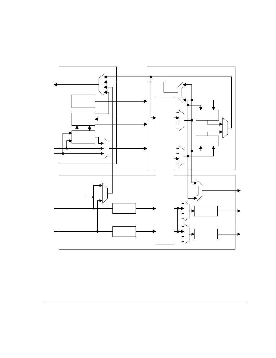
Integer Core
ARM DDI 0244C
Copyright © 2003 ARM Limited. All rights reserved.
2-3
Figure 2-1 Integer core block diagram
Integer unit
Load/store unit
Prefetch unit
Misprediction
Force prefetch 1
Prefetch
buffer
Branch phantom
Force prefetch 2
Branch
predictor/
return stack
PC
queue
Instruction
PC
Multiplier
Shift and
ALU
Decoded
load/store
instruction
Force prefetch 3
Dat
a
read
dat
a
(
DRD)
64
bi
t
s
I
n
s
t
ruc
t
i
o
n
r
ead
dat
a
(
I
R
D)
64
bi
t
s
I
n
s
t
ruc
t
i
o
n
addres
s
(
I
A
)
Dat
a
wri
t
e
dat
a
(
DWD)
Dat
a
addres
s
(
DA
)
Rotate and
sign extend
Rotate and
sign extend
Halfword
replicate
Halfword
replicate
Register
bank
W
A
B
L1
L2
S1
S2

Integer Core
2-4
Copyright © 2003 ARM Limited. All rights reserved.
ARM DDI 0244C
2.2
Pipeline
The ARM1026EJ-S pipeline has six stages to maximize instruction throughput:
Fetch
ICache access. Branch prediction for instructions that have already been
fetched. Prediction of fetch path ahead of execution of branch
instructions. The Fetch stage uses a First-In-First-Out (FIFO) prefetch
buffer that can hold up to four instructions.
Issue
Initial instruction decode. Can contain one instruction with up to one
branch in parallel.
Decode
Final instruction decode, register reads for ALU operation, data access
address calculation, forwarding, and initial interlock resolution. Can
contain one instruction with up to one branch in parallel.
Execute
Data processing shift, shift and saturate, ALU operation, first stage of
multiplications, flag setting, condition code check, branch mispredict
detection, first stage of store data register read, and DCache access
request.
Memory
Second stage of multiplications and saturations, second stage of store
data register read, and DCache memory access.
Write
Byte rotation, sign extension, register writes, and instruction retirement.
The Execute, Memory, and Write stages can simultaneously contain the following:
∑
a predicted branch
∑
an ALU, multiply or load/store instruction.
Figure 2-2 on page 2-5 shows the stages of the ARM1026EJ-S pipeline.

Integer Core
ARM DDI 0244C
Copyright © 2003 ARM Limited. All rights reserved.
2-5
Figure 2-2 Pipeline stages of the ARM1026EJ-S processor
LSU
pipeline
ALU
pipeline
ALU/MUL
register write
Saturation
Multiply(2)
ALU
operation/
Shift
Multiply(1)
Secondary
instruction
decode
Register read
ARM/Thumb/
Jazelle main
instruction
decode
Static branch
prediction
Instruction
fetch
Fetch
Issue
Decode
Execute
Memory
Write
Return stack
Data address
calculation
Byte rotate/
Sign extension
LSU register
write
Store data
register
read(2)
Data cache
access
Store data
register
read(1)
Data cache
request

Integer Core
2-6
Copyright © 2003 ARM Limited. All rights reserved.
ARM DDI 0244C
2.3
Prefetch unit
The prefetch unit operates in the Fetch stage of the pipeline. It can fetch 64 bits every
cycle from the ICache. It can only issue one 32-bit instruction per cycle to the integer
unit. Because it can fetch more instructions than it can issue, the prefetch unit puts
pending instructions in the prefetch buffer. While an instruction is in the prefetch buffer,
the branch prediction logic can decode it to see if it is a predictable branch.
Where possible, the branch prediction logic removes branches from the instruction
stream. If the branch is predicted to be taken, then the instruction address is redirected
to the branch target address. If the branch is predicted not to be taken, then the
instruction address continues to progress through the instructions following the branch
instruction. If the instruction following the branch is already in the prefetch buffer, it
can be issued in place of the branch and the branch effectively takes no cycles. When
there is not enough time to completely remove the branch, the fetch address is redirected
anyway, because this still helps to reduce the branch penalty.
The prefetch unit and branch prediction are described in detail in Chapter 5 Prefetch
Unit.

Integer Core
ARM DDI 0244C
Copyright © 2003 ARM Limited. All rights reserved.
2-7
2.4
Typical ALU/multiply operations
Figure 2-3 shows the stages of a typical data processing operation.
Figure 2-3 Pipeline stages of a typical ALU operation
Figure 2-4 shows the stages of a typical multiply operation. The MUL loops in the
Execute stage until it passes through the first part of the multiplier array enough times.
Then it progresses to the Memory stage where it passes once through the second half of
the array to produce the final result.
Figure 2-4 Pipeline stages of a typical multiply operation
LSU
pipeline
ALU
pipeline
Register
write
Cycle 6
Secondary
instruction
decode
Cycle 3
Main
instruction
decode
Cycle 2
Instruction
fetch
Cycle 1
Not used
Not used
Not used
Saturation
Cycle 5
ALU
operation/
Shift
Cycle 4
Not used
Register read
LSU
pipeline
ALU
pipeline
Main
instruction
decode
Cycle 2
Instruction
fetch
Cycle 1
Fetch
Issue
Decode
Execute
Memory
Write
Not used
Not used
Not used
Multiply 2
Cycle 4, 5
Multiply
Cycle 4, 5
Secondary
instruction
decode
Cycle 3
Register
write
Cycle 6, 7
Not used
Register read

Integer Core
2-8
Copyright © 2003 ARM Limited. All rights reserved.
ARM DDI 0244C
2.5
Load/store unit
If the data address is 64-bit aligned, the LSU can load or store two 32-bit registers per
transfer. This does not speed up single load or store instructions (LDR or STR) but it
does considerably speed up load and store multiple instructions (LDM and STM). Load
and store double instructions (LDRD and STRD) also take advantage of the available
bandwidth.
Accesses that are not 64-bit aligned have to take place over two cycles. If an LDM or
STM address is not 64-bit aligned, then only one 32-bit register is transferred on the first
access. After that, two registers per cycle can be transferred each cycle.
Single loads and all cycles of multiple loads and stores work in cooperation with the
integer unit. A DCache load access that misses stalls the LSU and integer unit until the
data is returned from the cache.
The LSU calculates the address for the data access using a dedicated adder. A separate
adder in the ALU calculates a base register write-back value if it is required.
The A and B register ports of the integer unit read the operands for both adders. For
complex, scaled-register addressing modes that require the barrel shifter, the ALU has
to calculate the shifted value. This costs one extra cycle.
The LSU has two dedicated register bank read ports, S1 and S2, and two dedicated write
ports, L1 and L2. These are used to read data to be stored and to write data that is loaded.

Integer Core
ARM DDI 0244C
Copyright © 2003 ARM Limited. All rights reserved.
2-9
2.6
Typical load/store operations
Figure 2-5 shows a simple LDR/STR operation that hits in the DCache.
Figure 2-5 Pipeline stages of a load or store operation
LSU
pipeline
ALU
pipeline
Base register
writeback
Cycle 6
Secondary
instruction
decode
Cycle 3
Main
instruction
decode
Cycle 2
Instruction
fetch
Cycle 1
Cycle 5
Writeback
value
calculation
Cycle 4
Store data
register read
Cycle 4
Memory
access
Cycle 5
Loaded data
register write
Cycle 6
Data address
calculation
Cycle 3
Memory
request
Register read
Integer Core
2-10
Copyright © 2003 ARM Limited. All rights reserved.
ARM DDI 0244C
Figure 2-6 shows the progression of an LDM/STM operation using the load/store
pipeline to complete. The LDM/STM iterates in the LSU pipeline until it completes.
Because any LDM/STM memory access can abort, the LSU stalls all integer pipeline
activity until the last LDM/STM memory access completes.
Figure 2-6 Pipeline stages of a load multiple or store multiple operation
See Chapter 21 Instruction Cycle Count for further details of instruction cycles and
timing.
LSU
pipeline
ALU
pipeline
Base register
writeback
Cycle 6
Register read
Cycle 3
Main
instruction
decode
Cycle 2
Instruction
fetch
Cycle 1
Cycle 5
Writeback
value
calculation
Cycle 4
Store data
register read
Cycle 4-7
Memory
access
Loaded data
register write
Cycle 5-8
Cycle 7-10
Data address
calculation
Cycle 3-6
Memory
request
Secondary
instruction
decode

ARM DDI 0244C
Copyright © 2003 ARM Limited. All rights reserved.
3-1
Chapter 3
Programmer's Model
This chapter describes the ARM1026EJ-S registers and provides information for
programming the microprocessor. It contains the following sections:
∑
About the programmer's model on page 3-2
∑
Program status registers on page 3-3
∑
About the CP15 system control coprocessor registers on page 3-5
∑
CP15 register descriptions on page 3-9
∑
CP15 instruction summary on page 3-70.

Programmer's Model
3-2
Copyright © 2003 ARM Limited. All rights reserved.
ARM DDI 0244C
3.1
About the programmer's model
The ARM1026EJ-S processor implements the ARMv5TEJ architecture. This includes
the:
∑
32-bit ARM instruction set
∑
16-bit Thumb instruction set
∑
8-bit Jazelle instruction set.
For details of both the ARM and Thumb instruction sets, and the ARM programmer's
model, see the ARM Architecture Reference Manual. For details of the Jazelle
instruction set and the Jazelle programmer's model, see the Jazelle VI Architecture
Reference Manual.
The ARM1026EJ-S programmer's model is the same as that described in the ARM
Architecture Reference Manual and the Jazelle VI Architecture Reference Manual, but
extended in the following ways:
∑
The Current Program Status Register, CPSR, and the Saved Program Status
Registers, SPSRs, have an additional J bit to indicate Jazelle state and an
additional A bit to mask imprecise aborts.
∑
The system control coprocessor, CP15, provides additional registers for system
configuration and control.
∑
The CP14 debug registers provide support for debug functionality. See Chapter 8
Debug for a description of the CP14 debug registers.

Programmer's Model
ARM DDI 0244C
Copyright © 2003 ARM Limited. All rights reserved.
3-3
3.2
Program status registers
To support exception handling, the ARM1026EJ-S processor has one CPSR and five
SPSRs. The Program Status Registers:
∑
hold information about the most recently performed ALU operation
∑
control enabling and disabling of interrupts
∑
set the processor operating mode.
Figure 3-1 Program Status Registers
3.2.1
The J bit
The J bit in the CPSR indicates when the ARM1026EJ-S processor is in Jazelle state.
When J is set, the processor is in Jazelle state. When J is clear, the processor is in ARM
or Thumb state, depending on the T bit.
Note
∑
Setting both J and T causes the next instruction executed to take the Undefined
Instruction exception. Entering the exception handler causes the processor to
enter ARM state, and the exception handler can detect that setting both J and T
caused the exception.
∑
The MSR instruction cannot be used to change the J bit in the CPSR.
∑
The position of the J bit avoids using the status or extension bytes in code run on
ARMv5TE or earlier processors. This ensures that operating system code that
uses the deprecated CPSR, SPSR, CPSR_all, or SPSR_all syntax for the
destination of an MSR instruction still works.
31
8 7
N
27
24
28
30 29
25
26
F
5
6
T
A I
Z C
Reserved
J
Reserved
V Q
Mode
4
0
23
9

Programmer's Model
3-4
Copyright © 2003 ARM Limited. All rights reserved.
ARM DDI 0244C
3.2.2
The A bit
An imprecise abort is separated from the instruction that caused the error response. The
abort can occur many cycles after the error-generating instruction retires. The AHB
error response leading to an imprecise abort can occur at a time when the processor is
already in Abort mode, or when the processor has entered the interrupt handler from
Abort mode.
To avoid the loss of the Abort mode state (R14_abt and SPSR_abt) in these cases, which
leads to the processor entering an unrecoverable state, the existence of a pending
imprecise abort must be held by the processor until a time when the Abort mode can
safely be entered.
The A mask is added to the CPSR to indicate that an imprecise abort can be accepted.
When the A bit is set, an imprecise abort is held until the mask is cleared. When the A
bit is cleared, a pending imprecise abort is recognized, and the abort is taken.
The A bit is set automatically on entry into Abort mode, IRQ mode, FIQ mode, and on
reset.
3.2.3
Other bits
All other bits of the CPSR and the SPSRs are as described in the ARM Architecture
Reference Manual.
Programmer's Model
ARM DDI 0244C
Copyright © 2003 ARM Limited. All rights reserved.
3-5
3.3
About the CP15 system control coprocessor registers
The programmer's model of the ARM1026EJ-S processor includes a system control
coprocessor, CP15, that provides additional registers for system configuration and
control.
3.3.1
Accessing CP15 registers
CP15 registers can be accessed only with MCR and MRC instructions in a privileged
mode. Figure 3-2 shows the MCR and MRC instruction format.
Figure 3-2 CP15 MCR and MRC instruction format
The assembly code for these instructions is:
MCR{cond} P15, opcode_1, Rd, CRn, CRm, opcode_2
MRC{cond} P15, opcode_1, Rd, CRn, CRm, opcode_2
In User mode, coprocessor instructions take the Undefined instruction trap. See the
ARM Architecture Reference Manual for a description of the MCR and MRC
instructions.
20
4
1
CRm
1111
Opcode_2
CRn
Rd
0
Opcode_1
1110
cond
31
28 27
24
19
16 15
12 11
8
3
0
23
21
7
5

Programmer's Model
3-6
Copyright © 2003 ARM Limited. All rights reserved.
ARM DDI 0244C
3.3.2
Summary of CP15 registers
Table 3-1 lists the 16 CP15 registers and their accessibility. The MMU/MPU enabled
column indicates whether you can access the register only when the MMU is enabled,
only when the MPU is enabled, or when either the MMU or MPU is enabled.
Table 3-1 CP15 register summary
Register
Register name
MMU or MPU
enabled
Access
CP15 c0
Device ID Register
Cache Type Register
TCM Status Register
MMU or MPU
MMU or MPU
MMU or MPU
Read-only
Read-only
Read-only
CP15 c1
Control Register
Auxiliary Control Register
MMU or MPU
MMU or MPU
Read/write
Read-only
CP15 c2
TTB Register
DCache Configuration Register
ICache Configuration Register
MMU only
MPU only
MPU only
Read/write
Read/write
Read/write
CP15 c3
Domain Access Control Register
Write Buffer Control Register
MMU only
MPU only
Read/write
Read/write
CP15 c4
Reserved
-
Undefined
CP15 c5
Data Fault Status Register when using MMU
Instruction Fault Status Register when using MMU
Data Extended Access Permission Register
Instruction Extended Access Permission Register
Data Standard Access Permission Register
Instruction Standard Access Permission Register
Data Fault Status Register when using MPU
Instruction Fault Status Register when using MPU
MMU only
MMU only
MPU only
MPU only
MPU only
MPU only
MPU only
MPU only
Read/write
Read/write
Read/write
Read/write
Read/write
Read/write
Read/write
Read/write
CP15 c5
Data Fault Address Register when using MMU
Instruction Fault Address Register when using MMU
Protection Region Registers 0-7
Data Fault Address Register when using MPU
Instruction Fault Address Register when using MPU
MMU only
MMU only
MPU only
MPU only
MPU only
Read/write
Read/write
Read/write
Read/write
Read/write
CP15 c7
Cache operations
MMU or MPU
Read/write
CP15 c8
TLB operations
MMU only
Write-only

Programmer's Model
ARM DDI 0244C
Copyright © 2003 ARM Limited. All rights reserved.
3-7
CP15 c9
DCache Lockdown Register
ICache Lockdown Register
DTCM Region Register
ITCM Region Register
MMU or MPU
MMU or MPU
MMU or MPU
MMU or MPU
Read/write
Read/write
Read/write
Read/write
CP15 c10
TLB Lockdown Register
MMU only
Read/write
CP15 c11
Reserved
-
Undefined
CP15 c12
Reserved
-
Undefined
CP15 c13
FCSE Process ID Register
Context ID Register
MMU only
MMU or MPU
Read/write
Read/write
CP15 c14
Reserved
-
Undefined
CP15 c15
Debug Override Register
Prefetch Unit Debug Override Register
Debug and Test Address Register
Memory Region Remap Register
MMU test operations
Cache Debug Control Register
MMU Debug Control Register
MMU or MPU
MMU or MPU
MMU or MPU
MMU or MPU
MMU only
MMU or MPU
MMU only
Read/write
Read/write
Read/write
Read/write
Read/write
Read/write
Read/write
Table 3-1 CP15 register summary (continued)
Register
Register name
MMU or MPU
enabled
Access

Programmer's Model
3-8
Copyright © 2003 ARM Limited. All rights reserved.
ARM DDI 0244C
3.3.3
Address types
The ARM processor uses three address types:
∑
Virtual Address (VA)
∑
Modified Virtual Address (MVA)
∑
Physical Address (PA).
Table 3-2 shows the parts of the ARM processor that use each address type.
Table 3-2 Address types
Processor unit
Address type
Integer unit
Virtual address
Caches and TLBs
Modified virtual address
TCM and AMBA bus
Physical address

Programmer's Model
ARM DDI 0244C
Copyright © 2003 ARM Limited. All rights reserved.
3-9
3.4
CP15 register descriptions
This section describes the CP15 registers:
∑
CP15 c0 Device ID Register on page 3-10
∑
CP15 c0 Cache Type Register on page 3-11
∑
CP15 c0 TCM Status Register on page 3-13
∑
CP15 c1 Control Register on page 3-14
∑
CP15 c1 Auxiliary Control Register on page 3-19
∑
CP15 c2 Translation Table Base Register on page 3-20
∑
CP15 c2 DCache and ICache Configuration Registers on page 3-21
∑
CP15 c3 Domain Access Control Register on page 3-23
∑
CP15 c3 Write Buffer Control Register on page 3-25
∑
CP15 c4 Reserved on page 3-26
∑
CP15 c5 Data and Instruction Fault Status Registers on page 3-26
∑
CP15 c5 Data and Instruction Extended Access Permission Registers on
page 3-29
∑
CP15 c5 Data and Instruction Standard Access Permission Registers on
page 3-31
∑
CP15 c5 Data and Instruction Fault Address Registers on page 3-33
∑
CP15 c5 Protection Region Registers on page 3-34
∑
CP15 c7 cache operations on page 3-36
∑
CP15 c8 TLB operations on page 3-40
∑
CP15 c9 DCache and ICache Lockdown Registers on page 3-41
∑
CP15 c9 DTCM and ITCM Region Registers on page 3-44
∑
CP15 c10 TLB Lockdown Register on page 3-46
∑
CP15 c11 Reserved on page 3-48
∑
CP15 c12 Reserved on page 3-48
∑
CP15 c13 FCSE Process ID Register on page 3-49
∑
CP15 c13 Context ID Register on page 3-52
∑
CP15 c14 Reserved on page 3-52
∑
CP15 c15 Debug Override Register on page 3-53
∑
CP15 c15 Prefetch Unit Debug Override Register on page 3-55
∑
CP15 c15 Debug and Test Address Register on page 3-56
∑
CP15 c15 Memory Region Remap Register on page 3-57
∑
CP15 c15 MMU test operations on page 3-60
∑
CP15 c15 Cache Debug Control Register on page 3-65
∑
CP15 c15 MMU Debug Control Register on page 3-67.

Programmer's Model
3-10
Copyright © 2003 ARM Limited. All rights reserved.
ARM DDI 0244C
3.4.1
CP15 c0 Device ID Register
The read-only Device ID Register contains the 32-bit ID code of the ARM1026EJ-S
processor,
0x4106A262
.
You can read the Device ID Register when using the MMU or the MPU
(MMUnMPU = 1 or 0). Use the following instruction to read the Device ID Register:
MRC p15, 0, Rd, c0, c0, {0, 3-7} ; read Device ID Register
When reading the Device ID Register, the opcode_2 field can be any value other than
1 or 2. Writing to the Device ID Register is Unpredictable.
Figure 3-3 shows the Device ID Register bit fields.
Figure 3-3 Device ID Register
Table 3-3 describes the bit fields of the Device ID Register.
Revision
Part number
Architecture
Variant
Implementer
31
24 23
20 19
16 15
4 3
0
Table 3-3 Encoding of the Device ID Register
Bit
Name
Definition
Reset state
[31:24]
Implementer
ASCII code for implementer's trademark. For example,
ARM Limited uses the code for the letter A,
0x41
.
0x41
[23:20]
Variant
Variant of the ARM processor.
0x0
[19:16]
Architecture
ARM architecture version v5TEJ.
0x6
[15:4]
Part number
Three-digit part number.
0xA26
[3:0]
Revision
Revision number of the ARM processor.
0x2
Programmer's Model
ARM DDI 0244C
Copyright © 2003 ARM Limited. All rights reserved.
3-11
3.4.2
CP15 c0 Cache Type Register
The read-only Cache Type Register reflects the type, size, associativity, and line length
of the ICache and the DCache.
You can read the Cache Type Register when using the MMU or the MPU
(MMUnMPU = 1 or 0). Use the following instruction to read the Cache Type Register:
MRC p15, 0, Rd, c0, c0, 1 ; read Cache Type Register
Writing to the Cache Type Register is Undefined.
Figure 3-4 shows the Cache Type Register bit fields.
Figure 3-4 Cache Type Register
Table 3-4 describes the bit fields of the Cache Type Register.
31
15
12 11
3
0
24 23
28
29
25
21
22
17
18
13
14
9
10
5
6
1
2
S
Reserved
Ctype
Size
Assoc
SBZ
Len
Reserved
Size
Assoc
SBZ
Len
ICache
DCache
Table 3-4 Encoding of the Cache Type Register
Bit
Name
Definition
Reset state
[31:29]
-
Reserved.
b000
[28:25]
Ctype
Cache class.
Write strategy: write-back.
Cache cleaning: c7 operations.
Cache lockdown: format C.
b1110
[24]
S
Harvard architecture.
1
[23:22]
-
Reserved.
b00
[21:18]
Size
DCache size. Implementation-defined:
b0011 = 4 KB
b0100 = 8 KB
b0101 = 16 KB
b0110 = 32 KB
b0111 = 64KB
b1000 = 128 KB.
Determined by
DCACHESIZE[3:0]
pins

Programmer's Model
3-12
Copyright © 2003 ARM Limited. All rights reserved.
ARM DDI 0244C
[17:15]
Assoc
DCache associativity. Four-way set-associative.
b010
[14]
-
Should Be Zero.
0
[13:12]
Len
DCache line length. Eight words per line.
b10
[11:10]
-
Reserved.
b00
[9:6]
Size
ICache size. Implementation-defined:
b0011 = 4 KB
b0100 = 8 KB
b0101 = 16 KB
b0110 = 32 KB
b0111 = 64KB
b1000 = 128 KB.
Determined by
ICACHESIZE[3:0]
pins
[5:3]
Assoc
ICache associativity. Four-way set-associative.
b010
[2]
-
Should Be Zero.
0
[1:0]
Len
ICache line length. Eight words per line.
b10
Table 3-4 Encoding of the Cache Type Register (continued)
Bit
Name
Definition
Reset state

Programmer's Model
ARM DDI 0244C
Copyright © 2003 ARM Limited. All rights reserved.
3-13
3.4.3
CP15 c0 TCM Status Register
The read-only TCM Status Register indicates the presence of a Data TCM (DTCM) and
an Instruction TCM (ITCM).
You can read the TCM Status Register when using the MMU or the MPU
(MMUnMPU = 1 or 0) with the following instruction:
MRC p15, 0, Rd, c0, c0, 2 ; read TCM Status Register
Writing to the TCM Status Register is Unpredictable.
Figure 3-5 shows the bit fields of the TCM Status Register.
Figure 3-5 TCM Status Register
Table 3-5 describes the bit fields of the TCM Status Register.
See Table 3-41 on page 3-45 for encoding of DRSIZE and IRSIZE bits in the DTCM
and ITCM Region Registers.
31
16 15
0
17
1
Unpredictable
Unpredictable
DTCM
ITCM
Table 3-5 Encoding of the TCM Status Register
Bit
Name
Definition
Reset state
[31:17]
-
Unpredictable.
0x0000
[16]
DTCM
DTCM present bit:
1 = DTCMSIZE pins are not b0000, meaning DTCM is present
0 = DTCMSIZE pins are b0000, meaning DTCM is not present.
Determined by
DTCMSIZE[3:0]
pins
[15:1]
-
Unpredictable.
0x0000
[0]
ITCM
ITCM present bit:
1 = ITCMSIZE pins are not b0000, meaning ITCM is present
0 = ITCMSIZE pins are b0000, meaning ITCM is not present.
Determined by
ITCMSIZE[3:0]
pins

Programmer's Model
3-14
Copyright © 2003 ARM Limited. All rights reserved.
ARM DDI 0244C
3.4.4
CP15 c1 Control Register
The read/write Control Register:
∑
enables reading IRQ vector addresses from the VIC port
∑
enables relocation of the IRQ vector address
∑
selects whether the T bit is set by a load PC operation
∑
selects random or round-robin victim replacement
∑
selects high-address or low-address vector locations
∑
enables the ICache and DCache
∑
enables branch prediction
∑
enables ROM protection and system protection
∑
selects big-endian or little-endian operation
∑
enables fault checking of address alignment
∑
enables the MMU
∑
enables the MPU.
You can access the Control Register when using the MMU or the MPU
(MMUnMPU = 1 or 0) with the instructions in Table 3-6.
Use a read-modify-write sequence when changing the Control Register.
All defined control bits are cleared on reset except:
∑
The V bit is cleared at reset if the HIVECSINIT signal is LOW or set if the
HIVECSINIT signal is HIGH.
∑
The B bit is cleared at reset if the BIGENDINIT signal is LOW or set if the
BIGENDINIT signal is HIGH.
Table 3-6 Control Register instructions
Instruction
Operation
MRC p15, 0, Rd, c1, c0, 0
Read Control Register
MCR p15, 0, Rd, c1, c0, 0
Write Control Register

Programmer's Model
ARM DDI 0244C
Copyright © 2003 ARM Limited. All rights reserved.
3-15
Figure 3-6 shows the Control Register bit fields.
Figure 3-6 Control Register
Table 3-7 describes the Control Register bit fields.
31
16 15
12 11
8 7
3
0
SBZ
24 23
19
25
17
18
13
14
V
9
10
R
SBO
6
C
1
2
A
S B
I Z
SBZ
M
VE
SBO
SBZ
SBO
LT
RR
SBZ
Table 3-7 Encoding of the Control Register
Bit
Name
Definition
Reset state
[31:25]
-
Reading returns an Unpredictable value. When written, Should Be Zero
or a value read from bits [31:25] on the same processor.
Zeros
[24]
VE
Vector Interrupt Controller (VIC) enable bit:
1 = processor reads IRQ vector address from VIC port
0 = processor reads IRQ vector address from
0x00000018
or
0xFFFF0018
.
0
[23:19]
-
Should Be Zero.
Zeros
[18]
-
Should Be One.
1
[17]
-
Should Be Zero.
0
[16]
-
Should Be One.
1
[15]
LT
Load PC Thumb disable bit:
1 = loading PC does not set T bit
0 = loading PC sets T bit.
0
[14]
RR
ICache and DCache round-robin replacement bit:
1 = round-robin replacement enabled
0 = random replacement.
0
[13]
V
Exception vector location bit:
1 = vector address range is
0xFFFF0000
to
0xFFFF001C
0 = vector address range is
0x00000000
to
0x0000001C
.
Determined by
HIVECSINIT
pin

Programmer's Model
3-16
Copyright © 2003 ARM Limited. All rights reserved.
ARM DDI 0244C
[12]
I
ICache enable bit:
1 = ICache enabled
0 = ICache disabled.
0
[11]
Z
Branch prediction enable bit:
1 = branch prediction enabled
0 = branch prediction disabled.
0
[10]
-
Should Be Zero.
0
[9]
R
MMU ROM protection enable bit:
1 = ROM protection enabled
0 = ROM protection disabled.
Valid only when using the MMU (MMUnMPU = 1).
0
[8]
S
MMU system protection enable bit:
1 = MMU protection enabled
0 = MMU protection disabled.
Valid only when using the MMU (MMUnMPU = 1).
0
[7]
B
Big-endian bit:
1 = big-endian operation
0 = little-endian operation.
Determined by
BIGENDINIT
pin
[6:3]
-
Should Be One.
0xF
[2]
C
DCache enable bit:
1 = DCache enabled
0 = DCache disabled.
0
[1]
A
Address alignment fault checking enable bit:
1 = fault checking of address alignment enabled
0 = fault checking of address alignment disabled.
0
[0]
M
MMU enable bit when MMUnMPU = 1
or MPU enable bit when MMUnMPU = 0:
1 = MMU or MPU enabled
0 = MMU or MPU disabled.
0
Table 3-7 Encoding of the Control Register (continued)
Bit
Name
Definition
Reset state

Programmer's Model
ARM DDI 0244C
Copyright © 2003 ARM Limited. All rights reserved.
3-17
Effects of the Control Register on caches
The bits that directly affect ICache and DCache behavior are:
∑
the M bit
∑
the C bit
∑
the I bit
∑
the RR bit.
When the TCM regions are disabled, the caches behave as shown in Table 3-8.
If either the DCache or ICache is disabled, the contents of that cache are not accessed.
If the cache is subsequently re-enabled, the contents are unchanged. To guarantee
memory coherency, the DCache must be cleaned of dirty data before it is disabled.
Table 3-8 Effects of Control Register on caches
Cache
MMU/MPU
Processor behavior
ICache
disabled
Enabled or
disabled
All instruction fetches are from external memory (AHB).
ICache
enabled
Disabled
All instruction fetches cachable. No protection checks done. VA = MVA = PA.
ICache
enabled
Enabled
Instruction fetches cachable or noncachable. Protection checks done.
When using MMU, all addresses remapped from VA to PA, depending on MMU page table
entry. VA translated to MVA, MVA remapped to PA.
When using MPU, VA = MVA = PA.
DCache
disabled
Enabled or
disabled
All data accesses to external memory (AHB).
DCache
enabled
Disabled
All data accesses noncachable and nonbufferable. VA = MVA = PA.
DCache
enabled
Enabled
All data accesses cachable or noncachable. Protection checks done.
When using MMU, all addresses remapped from VA to PA, depending on MMU page table
entry. VA translated to MVA, MVA remapped to PA.
When using MPU, VA = MVA = PA.

Programmer's Model
3-18
Copyright © 2003 ARM Limited. All rights reserved.
ARM DDI 0244C
Effects of the Control Register on the TCM interface
The Control Register M bit and the E bit in the ITCM or DTCM Register directly affect
the behavior of the TCM interface as Table 3-9 shows.
Table 3-9 Effects of Control Register on TCM interface
TCM
MMU or MPU
Cache
Processor behavior
ITCM
disabled
Disabled
ICache
disabled
All instruction fetches from external memory (AHB).
ITCM
enabled
Disabled
ICache
disabled
All instruction fetches from TCM interface or from external memory (AHB),
depending on base address in ITCM Region Register. No protection checks
done. VA = MVA = PA.
ITCM
enabled
Disabled
ICache
enabled
All instruction fetches from TCM interface or from ICache, depending on base
address in ITCM Region Register. No protection checks done.
VA = MVA = PA.
ITCM
enabled
Enabled
ICache
enabled
All instruction fetches from TCM interface or from the ICache interface or
AHB interface, depending on base address in ITCM Region Register.
Protection checks are made.
When using MMU, all addresses remapped from VA to PA, depending on the
page entry. VA is translated to MVA, and MVA is remapped to PA.
When using MPU, VA = MVA = PA.
DTCM
disabled
Disabled
DCache
disabled
All data accesses are to external memory (AHB).
DTCM
enabled
Disabled
DCache
disabled
All data accesses to TCM interface or to external memory, depending on base
address in DTCM Region Register. No protection checks done.
VA = MVA = PA.
DTCM
enabled
Disabled
DCache
enabled
All data accesses to TCM interface or to external memory, depending on base
address in DTCM Region Register. VA = MVA = PA.
DTCM
enabled
Enabled
DCache
enabled
All data accesses from either TCM interface or DCache interface or AHB
interface, depending on base address in DTCM Region Register. Protection
checks done.
When using MMU, all addresses remapped from VA to PA, depending on page
entry. VA translated to MVA, and MVA remapped to PA.
When using MPU, VA = MVA = PA.

Programmer's Model
ARM DDI 0244C
Copyright © 2003 ARM Limited. All rights reserved.
3-19
3.4.5
CP15 c1 Auxiliary Control Register
The read-only Auxiliary Control Register reflects implementation-specific pin
configurations.
You can read the Auxiliary Control Register when using the MMU or the MPU
(MMUnMPU = 1 or 0) with the following instruction:
MRC p15, 0, Rd, c1, c0, 1
; read Auxiliary Control Register
Figure 3-7 shows the bit fields of the Auxiliary Control Register.
Figure 3-7 Auxiliary Control Register
Table 3-10 describes the bit fields of the Auxiliary Control Register.
VALInIMPL
DAHBSZCFG
IAHBSZCFG
MxUCFG
31
4 3
0
SBZ
1
2
Table 3-10 Encoding of the Auxiliary Control Register
Bit
Name
Definition
Reset state
[31:4]
-
Should Be Zero.
0x0000000
[3]
VALInIMPL
Indicates whether processor is ARM-internal validation model
or partner-specific fixed-implementation model:
1 = validation model
0 = implementation model.
Determined by
implementation
[2]
DAHBSZCFG
Indicates whether data AHB is 64 bits or 32 bits wide:
1 = 64-bit DAHB
0 = 32-bit DAHB.
Determined by
D64n32 pin
[1]
IAHBSZCFG
Indicates whether instruction AHB is 64 bits or 32 bits wide:
1 = 64-bit IAHB
0 = 32-bit IAHB.
Determined by
I64n32 pin
[0]
MxUCFG
Indicates whether MMU or MPU is enabled:
1 = MMU enabled
0 = MPU enabled.
Determined by
MMUnMPU pin

Programmer's Model
3-20
Copyright © 2003 ARM Limited. All rights reserved.
ARM DDI 0244C
3.4.6
CP15 c2 Translation Table Base Register
The read/write Translation Table Base Register, TTBR, contains the pointer to the level
1 translation table and the cachable and bufferable bits for the page tables on AHB.
You can access the TTBR only when using the MMU (MMUnMPU = 1) with the
instructions in Table 3-11.
Figure 3-8 shows the TTBR bit fields.
Figure 3-8 Translation Table Base Register
Table 3-12 describes the TTBR bit fields.
Table 3-11 Translation Table Base Register instructions
Instruction
Operation
MRC p15, 0, Rd, c2, c0, 0
Read Translation Table Base Register
MCR p15, 0, Rd, c2, c0, 0
Write Translation Table Base Register
SBZ
L2C
L2B
31
4 3
0
13
14
5
2
Translation table base
SBZ
Table 3-12 Encoding of the Translation Table Base Register
Bit
Name
Definition
Reset state
[31:14]
Translation table base
Base address of level 1 page table.
Zeros
[13:5]
-
Should Be Zero.
Zeros
4
L2C
Cachable bit for level 2 page table walk. See Table 3-13
on page 3-21.
0
3
L2B
Bufferable bit for level 2 page table walk. See Table 3-13
on page 3-21.
0
[2:0]
-
Should Be Zero.
b000

Programmer's Model
ARM DDI 0244C
Copyright © 2003 ARM Limited. All rights reserved.
3-21
Table 3-13 shows how the L2C and L2B bits control the HPROT[3:0] signals and the
attributes of level 2 page table walks.
3.4.7
CP15 c2 DCache and ICache Configuration Registers
The read/write DCache Configuration Register, DCCR, and ICache Configuration
Register, ICCR, contain the cachable bits for the eight protection regions. Each of the
eight cachable bits controls one of the eight protection regions.
You can access the DCCR and ICCR only when using the MPU (MMUnMPU = 0)
with the instructions in Table 3-14.
Table 3-13 L2C and L2B encoding
TTBR[4:3]
HPROT[3:0]
Level 2 page table walk attributes
b00
b0011
Privileged NCNB data access
b01
-
Unpredictable
b10
b1011
Privileged write-through data access
b11
b1111
Privileged write-back data access
Table 3-14 DCache and ICache Configuration Register instructions
Instruction
Operation
MRC p15, 0, Rd, c2, c0, 0
Read DCache Configuration Register
MCR p15, 0, Rd, c2, c0, 0
Write DCache Configuration Register
MRC p15, 0, Rd, c2, c0, 1
Read ICache Configuration Register
MCR p15, 0, Rd, c2, c0, 1
Write ICache Configuration Register

Programmer's Model
3-22
Copyright © 2003 ARM Limited. All rights reserved.
ARM DDI 0244C
Figure 3-9 shows the DCCR and ICCR bit fields.
Figure 3-9 DCache and ICache Configuration Registers
Table 3-15 describes the bit fields of the DCache and ICache Configuration Registers.
C7
C0
C1
C2
C3
C4
C5
C6
31
8 7
4 3
0
5
6
1
2
SBZ
Table 3-15 Encoding of the DCache and ICache Configuration Registers
Bit
Name
Definition
Reset state
[7]-[0]
C7-C0
Cachable bits:
1 = memory region is cachable
0 = memory region is noncachable.
0

Programmer's Model
ARM DDI 0244C
Copyright © 2003 ARM Limited. All rights reserved.
3-23
3.4.8
CP15 c3 Domain Access Control Register
The read/write Domain Access Control Register, DACR, contains 16 two-bit domain
access control fields. Each field defines the access permissions for one of the 16
domains, D15-D0.
You can access the DACR only when using the MMU (MMUnMPU = 1) with the
instructions in Table 3-16.
Figure 3-10 shows the DACR bit fields.
Figure 3-10 Domain Access Control Register
Table 3-17 describes the DACR bit fields.
The domain access control fields specify whether or not to check the Access Permission
(AP) bits for each domain. When using the MMU, the AP bits reside in the translation
table level two descriptor entries for large, tiny, or small pages and in the level one
descriptor entries for sections.
Table 3-16 Domain Access Control Register instructions
Instruction
Operation
MRC p15, 0, Rd, c3, c0, 0
Read Domain Access Control Register
MCR p15, 0, Rd, c3, c0, 0
Write Domain Access Control Register
D0
D1
D3
D2
D4
D5
D8
D7
D6
D9
D11 D10
D13 D12
D15 D14
31 30 29 28 27 26 25 24 23 22 21 20 19 18 17 16 15 14 13 12 11 10 9 8 7 6 5 4 3 2 1 0
Table 3-17 Encoding of the Domain Access Control Register
Bit
Name
Definition
Reset state
[31:30]-[1:0]
D15-D0
Domain access control for domains 15-0:
b00 = No access. Access generates domain fault.
b01 = Client access. Access permissions are checked.
b10 = Reserved. Behaves as no access domain.
b11 = Manager access. Access permissions are not checked.
b00

Programmer's Model
3-24
Copyright © 2003 ARM Limited. All rights reserved.
ARM DDI 0244C
Note
When the MPU is enabled, the AP bits have their own CP15 register space. See:
∑
CP15 c5 Data and Instruction Extended Access Permission Registers on
page 3-29
∑
CP15 c5 Data and Instruction Standard Access Permission Registers on
page 3-31.
Table 3-18 shows the access permissions when using the MMU.
Table 3-18 Access permission summary when using the MMU
AP
CP15
S bit
CP15
R bit
Supervisor
User
Access
b00
0
0
-
-
Permission fault
b00
1
0
Read
-
Read-only in Supervisor mode
b00
0
1
Read
Read
Permission fault on writes
b00
1
1
Reserved
Reserved
Permission fault on reads or writes
b01
-
-
Read/write
-
Permission fault on reads or writes in User mode
b10
-
-
Read/write
Read
Read-only in User mode
b11
-
-
Read/write
Read/write
All accesses permissible
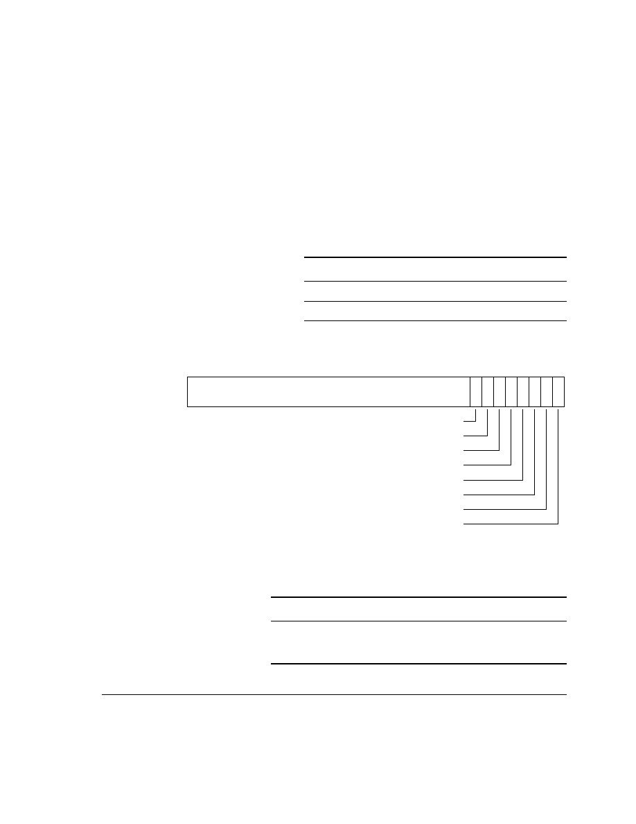
Programmer's Model
ARM DDI 0244C
Copyright © 2003 ARM Limited. All rights reserved.
3-25
3.4.9
CP15 c3 Write Buffer Control Register
The read/write Write Buffer Control Register, WBCR, contains the bufferable bits for
data accesses to protection regions 0-7. Each of the eight bits controls one of the eight
protection regions.
You can access the WBCR only when using the MPU (MMUnMPU = 0) with the
instructions in Table 3-19.
Figure 3-11 shows the WBCR bit fields.
Figure 3-11 Write Buffer Control Register
Table 3-20 describes the bit fields of the WBCR.
Table 3-19 Write Buffer Control Register instructions
Instruction
Operation
MRC p15, 0, Rd, c3, c0, 0
Read Write Buffer Control Register
MCR p15, 0, Rd, c3, c0, 0
Write Write Buffer Control Register
7
4 3
0
SBZ
B6
5
6
B5
B2
1
2
B1
B4
B3
B7
B0
31
8
Table 3-20 Encoding of the Write Buffer Control Register
Bit
Name
Definition
Reset state
[7]-[0]
B7-B0
Bufferable bits:
1 = protection region is bufferable
0 = protection region is nonbufferable.
0

Programmer's Model
3-26
Copyright © 2003 ARM Limited. All rights reserved.
ARM DDI 0244C
3.4.10
CP15 c4 Reserved
CP15 c4 accesses take the Undefined exception trap.
3.4.11
CP15 c5 Data and Instruction Fault Status Registers
The read/write Data Fault Status Register, DFSR, contains the source of the last data
fault. The DFSR indicates the domain and type of access being attempted when an abort
occurred. You can use the DFSR to check all Data Aborts and watchpoints and to map
a debug event to a watchpoint.
The read/write Instruction Fault Status Register, IFSR, contains the source of the last
instruction fault. The IFSR indicates the domain and type of access being attempted
when an abort occurred. You can use the IFSR to check all Prefetch Aborts and
breakpoints and to map a debug event to a breakpoint.
You can access the DFSR and IFSR when using the MMU or the MPU
(MMUnMPU = 1 or 0) with the instructions in Table 3-21.
It can be useful for a debugger to restore the value in the DFSR or IFSR by writing to
it. Use a read-modify-write sequence to change the DFSR or IFSR.
Table 3-21 Data and Instruction Fault Status Register instructions
MMU or MPU enabled
Instruction
Operation
MMU
MRC p15, 0, Rd, c5, c0, 0
Read Data Fault Status Register
MCR p15, 0, Rd, c5, c0, 0
Write Data Fault Status Register
MPU
MCR p15, 0, Rd, c5, c0, 4
Read Data Fault Status Register
MCR p15, 0, Rd, c5, c0, 4
Write Data Fault Status Register
MMU
MRC p15, 0, Rd, c5, c0, 1
Read Instruction Fault Status Register
MCR p15, 0, Rd, c5, c0, 1
Write Instruction Fault Status Register
MPU
MRC p15, 0, Rd, c5, c0, 5
Read Instruction Fault Status Register
MRC p15, 0, Rd, c5, c0, 5
Write Instruction Fault Status Register

Programmer's Model
ARM DDI 0244C
Copyright © 2003 ARM Limited. All rights reserved.
3-27
Figure 3-12 shows the DFSR and IFSR bit fields.
Figure 3-12 Data and Instruction Fault Status Registers
Table 3-22 describes the DFSR and IFSR bit fields.
Table 3-23 on page 3-28 lists the types of fault in order of priority from highest (0) to
lowest (12).
8 7
4 3
0
SBZ
9
10
SBZ
31
11
Ext
Domain or protection region
Status
Table 3-22 Encoding of the Data and Instruction Fault Status Registers
Bit
Name
Definition
Reset state
[31:11]
-
Should Be Zero.
0x00000
[10]
Ext
Fault status extension.
Undefined
[9:8]
-
Should Be Zero.
b00
[7:4]
Domain or
Protection region
When using MMU:
Domain (D15-D0) being accessed when a fault occurred.
When using MPU:
Protection region (7-0) being accessed when a fault occurred.
Undefined
[3:0]
Status
Fault status or type of fault generated (see Table 3-23 on
page 3-28).
Undefined

Programmer's Model
3-28
Copyright © 2003 ARM Limited. All rights reserved.
ARM DDI 0244C
Table 3-23 MMU and MPU faults
Fault type
Status
[10], [3:0]
FSR updated
Priority
Valid
IFSR
DFSR
MMU
MPU
MMU
MPU
Imprecise external abort
1, b0110
Yes
Yes
0
0
Yes
Yes
Alignment fault
0, b0001
No
Yes
1
1
Yes
Yes
TLB miss or MPU miss
0, b0000
Yes
Yes
2
2
Yes
Yes
Level 1 translation precise external abort
0, b1100
Yes
Yes
3
-
Yes
No
Level 1 section translation fault
0, b0101
Yes
Yes
4
-
Yes
No
Level 2 translation precise external abort
0, b1110
Yes
Yes
5
-
Yes
No
Level 2 page translation fault
0, b0111
Yes
Yes
6
-
Yes
No
Section domain fault
0, b1001
Yes
Yes
7
-
Yes
No
Page domain fault
0, b1011
Yes
Yes
8
-
Yes
No
MMU: Section access permission fault
MPU: Access permission fault
0, b1101
Yes
Yes
9
3
Yes
Yes
Page access permission fault
0, b1111
Yes
Yes
10
-
Yes
No
Nontranslation precise external abort
0, b1000
Yes
Yes
11
4
Yes
Yes
Debug breakpoint or watchpoint
0, b0010
Yes
Yes
12
5
Yes
Yes
Reserved
0, b0011
0, b1010
0, b0100
0, b0110
1, b0100
1, b1000
-
-
-
-
-
-

Programmer's Model
ARM DDI 0244C
Copyright © 2003 ARM Limited. All rights reserved.
3-29
3.4.12
CP15 c5 Data and Instruction Extended Access Permission Registers
Note
There are two formats for specifying access permissions of memory protection regions:
∑
extended format
∑
standard format.
Use the DEAPR and IEAPR to specify access permissions in extended format. For
specifying access permissions in standard format, see CP15 c5 Data and Instruction
Standard Access Permission Registers on page 3-31.
Programming the access permissions in extended format and then reprogramming them
in standard format is equivalent to programming bits APn[3:2] in the DEAPR or IEAPR
to b00 (see Table 3-26 on page 3-30).
The read/write Data Extended Access Permission Register, DEAPR, and Instruction
Extended Access Permission Register, IEAPR, contain the data and instruction access
permission fields in extended format for memory protection regions 7-0.
You can access the DEAPR and IEAPR only when using the MPU (MMUnMPU = 0)
with the instructions in Table 3-24.
Figure 3-13 shows the DEAPR and IEAPR bit fields.
Figure 3-13 Data and Instruction Extended Access Permission Registers
Table 3-24 DEAPR and IEAPR instructions
Instruction
Operation
MRC p15, 0, Rd, c5, c0, 2
Read Data Extended Access Permission Register
MCR p15, 0, Rd, c5, c0, 2
Write Data Extended Access Permission Register
MRC p15, 0, Rd, c5, c0, 3
Read Instruction Extended Access Permission Register
MCR p15, 0, Rd, c5, c0, 3
Write Instruction Extended Access Permission Register
AP7
31
28
AP6
27
24
AP5
20
23
16
19
AP4
AP3
15
12 11
8
AP2
7
4 3
0
AP1
AP0

Programmer's Model
3-30
Copyright © 2003 ARM Limited. All rights reserved.
ARM DDI 0244C
Table 3-25 describes the DEAPR and IEAPR bit fields.
Table 3-26 lists the extended access permission codes.
Note
You must program either the DEAPR and IEAPR or the DSAPR and ISAPR before
enabling the MPU. On reset, the values in all access permission registers are Undefined,
and the MPU is disabled. Enabling the MPU before programming the access permission
registers results in Unpredictable access permissions.
Table 3-25 Encoding of the DEAPR and IEAPR
Bit
Name
Definition
Reset state
[31:28]-[3:0]
AP7-AP0
Extended format access permission bits for protection regions 7-0
Undefined
Table 3-26 Encoding of the extended access permission bit fields
AP{7-0} [3:0]
Privileged mode
User mode
b0000
No access
No access
b0001
Read/write
No access
b0010
Read/write
Read
b0011
Read/write
Read/write
b0100
Unpredictable
Unpredictable
b0101
Read
No access
b0110
Read
Read
b0111
Unpredictable
Unpredictable
b1xxx
Unpredictable
Unpredictable

Programmer's Model
ARM DDI 0244C
Copyright © 2003 ARM Limited. All rights reserved.
3-31
3.4.13
CP15 c5 Data and Instruction Standard Access Permission Registers
Note
There are two formats for specifying access permissions of memory protection regions:
∑
standard format
∑
extended format.
Use the DSAPR and ISAPR to specify access permissions in standard format. For
specifying access permissions in extended format, see CP15 c5 Data and Instruction
Extended Access Permission Registers on page 3-29.
Programming the access permissions in extended format and then reprogramming them
in standard format is equivalent to programming bits APn[3:2] in the DEAPR or IEAPR
to b00 (see Table 3-26 on page 3-30).
The read/write Data Standard Access Permission Register, DSAPR, and Instruction
Standard Access Permission Register, ISAPR, contain the data and instruction access
permission fields in standard format for protection regions 0-7.
You can access the DSAPR and ISAPR only when using the MPU (MMUnMPU = 0)
with the instructions in Table 3-27.
Figure 3-14 shows the DSAPR and ISAPR bit fields.
Figure 3-14 Data and Instruction Standard Access Permission Registers
Table 3-27 DSAPR and ISAPR instructions
Instruction
Operation
MRC p15, 0, Rd, c5, c0, 0
Read Data Standard Access Permission Register
MCR p15, 0, Rd, c5, c0, 0
Write Data Standard Access Permission Register
MRC p15, 0, Rd, c5, c0, 1
Read Instruction Standard Access Permission Register
MCR p15, 0, Rd, c5, c0, 1
Write Instruction Standard Access Permission Register
15
12
SBZ
13
14
31
16
0
1
3 2
4
5
6
7
8
9
11 10
AP7 AP6
AP4 AP3 AP2 AP1 AP0
AP5

Programmer's Model
3-32
Copyright © 2003 ARM Limited. All rights reserved.
ARM DDI 0244C
Table 3-28 describes the DSAPR and ISAPR bit fields.
Table 3-29 lists the standard access permission codes.
Note
You must program either the DSAPR and ISAPR or the DEAPR and IEAPR before
enabling the MPU. On reset, the values in all access permission registers are Undefined,
and the MPU is disabled. Enabling the MPU before programming the access permission
registers results in Unpredictable access permissions.
Table 3-28 Encoding of the DSAPR and ISAPR
Bit
Name
Definition
Reset state
[31:16]
-
Should Be Zero
0x0000
[15:14]-[1:0]
AP7-AP0
Standard format access permission bits for protection regions 7-0
Undefined
Table 3-29 Encoding of the standard access permission bit fields
AP{7-0} [1:0]
Privileged mode
User mode
b00
No access
No access
b01
Read/write
No access
b10
Read/write
Read
b11
Read/write
Read/write

Programmer's Model
ARM DDI 0244C
Copyright © 2003 ARM Limited. All rights reserved.
3-33
3.4.14
CP15 c5 Data and Instruction Fault Address Registers
The read/write Data Fault Address Register, DFAR, contains the MVA of the memory
access that caused a Data Abort.
The read/write Instruction Fault Address Register, IFAR, contains the MVA of the
memory access which caused either a watchpoint or a Data Abort. The address is PC + 8
in ARM state or PC + 4 in Thumb state.
You can access the DFAR and IFAR when using the MMU or the MPU
(MMUnMPU = 1 or 0) with the instructions in Table 3-30.
It can be useful for a debugger to restore the value in DFAR or IFAR by writing to it.
Figure 3-15 shows the DFAR and IFAR bit fields.
Figure 3-15 Data and Instruction Fault Address Registers
The reset state of the Data and Instruction Fault Address Registers is Undefined.
Table 3-30 DFAR and IFAR instructions
MMU or MPU enabled
Instruction
Operation
MMU
MRC p15, 0, Rd, c6, c0, 0
Read Data Fault Address Register
MCR p15, 0, Rd, c6, c0, 0
Write Data Fault Address Register
MPU
MRC p15, 0, Rd, c6, c0, 4
Read Data Fault Address Register
MCR p15, 0, Rd, c6, c0, 4
Write Data Fault Address Register
MMU
MRC p15, 0, Rd, c6, c0, 1
Read Instruction Fault Address Register
MCR p15, 0, Rd, c6, c0, 1
Write Instruction Fault Address Register
MPU
MRC p15, 0, Rd, c6, c0, 5
Read Instruction Fault Address Register
MCR p15, 0, Rd, c6, c0, 5
Write Instruction Fault Address Register
31
0
MVA of data or instruction fault

Programmer's Model
3-34
Copyright © 2003 ARM Limited. All rights reserved.
ARM DDI 0244C
3.4.15
CP15 c5 Protection Region Registers
The read/write Protection Region Registers, PRR0-7, define the base address and size
of the eight protection regions.
You can access PRR0-7 only when using the MPU (MMUnMPU = 0) with the
instructions in Table 3-31.
Note
When the MMU is enabled, accessing a Protection Region Register takes the Undefined
instruction trap.
Figure 3-16 shows the PRR bit fields.
Figure 3-16 Protection Region Registers 0-7
Table 3-32 describes the PRR bit fields.
Table 3-31 Protection Region Registers instructions
Instruction
Operation
MRC p15, 0, Rd, c6, c{0-7}, 0
Read Protection Region Register
MCR p15, 0, Rd, c6, c{0-7}, 0
Write Protection Region Register
0
Region base address
Region size
SBZ
E
31
12 11
6 5
1
Table 3-32 Encoding of the Protection Region Registers
Bit
Name
Definition
Reset state
[31:12]
Region
base address
Base address of protection region. Must be aligned
to size boundary of protection region.
Undefined
[11:6]
-
Should Be Zero.
Zeros

Programmer's Model
ARM DDI 0244C
Copyright © 2003 ARM Limited. All rights reserved.
3-35
Note
Writing a value less than b01011 to the region size field causes Unpredictable behavior.
[5:1]
Region size
Size of protection region:
b00000-b01010 = reserved
b01011 = 4KB
b01100 = 8KB
b01101 = 16KB
b01110 = 32KB
b01111 = 64KB
b10000 = 128KB
b10001 = 256KB
b10010 = 512KB
b10011 = 1MB
b10100 = 2MB
b10101 = 4MB
b10110 = 8MB
b10111 = 16MB
b11000 = 32MB
b11001 = 64MB
b11010 = 128MB
b11011 = 256MB
b11100 = 512MB
b11101 = 1GB
b11110 = 2GB
b11111 = 4GB.
Undefined
0
E
Protection region enable bit:
1 = protection region enabled
0 = protection region disabled.
0
Table 3-32 Encoding of the Protection Region Registers (continued)
Bit
Name
Definition
Reset state

Programmer's Model
3-36
Copyright © 2003 ARM Limited. All rights reserved.
ARM DDI 0244C
3.4.16
CP15 c7 cache operations
Use MCR and MRC instructions with a CRn of c7 to perform cache operations and
system control operations:
∑
cache operations:
--
clean
--
invalidate
--
clean and invalidate
--
test and clean
--
test, clean, and invalidate.
∑
system control operations:
--
wait for interrupt
--
drain pending write buffer
--
prefetch ICache line.
Most invalidate operations and clean operations support accesses in the MVA and
set/way formats. The address for the operation is stored in the ARM10 destination
register, Rd.
You can perform cache operations and system control operations using CP15 c7 when
using the MMU or the MPU (MMUnMPU = 1 or 0) with the instructions in Table 3-33.
Table 3-33 Cache operation instructions
Instruction
Operation
MCR p15, 0, Rd, c7, c5, 0
MCR p15, 0, Rd, c7, c5, 1
MCR p15, 0, Rd, c7, c5, 2
Invalidate entire ICache.
Invalidate ICache line, MVA format.
Invalidate ICache line, set/way format.
MCR p15, 0, Rd, c7, c6, 0
MCR p15, 0, Rd, c7, c6, 1
MCR p15, 0, Rd, c7, c6, 2
Invalidate entire DCache. Invalidates clean and dirty data.
Invalidate DCache line, MVA format. Invalidates clean and dirty data.
Invalidate DCache line, set/way format. Invalidates clean and dirty data.
MCR p15, 0, Rd, c7, c7, 0
Invalidate entire DCache and ICache. Invalidates clean and dirty data.
MCR p15, 0, Rd, c7, c10, 1
MCR p15, 0, Rd, c7, c10, 2
Clean DCache line, MVA format. Writes line to memory if valid and dirty. Marks line as
not dirty. Valid bit is unchanged.
Clean DCache line, set/way format. Writes line to memory if valid and dirty. Marks line
as not dirty. Valid bit is unchanged.
MCR p15, 0, Rd, c7, c14, 1
Clean and invalidate DCache line, MVA format. Writes line to memory if valid and dirty.
Marks line as invalid and not dirty.
MCR p15, 0, Rd, c7, c14, 2
Clean and invalidate DCache line, set/way format. Writes line to memory if valid and
dirty. Marks line as invalid and not dirty.

Programmer's Model
ARM DDI 0244C
Copyright © 2003 ARM Limited. All rights reserved.
3-37
Dirty data is data that has been modified in the cache but not yet copied back to main
memory.
ICache prefetch operations are performed requested-word-first.
MRC p15, 0, R15, c7, c10, 3
Test and clean DCache. Must have r15 as destination register. Does not change PC.
Updates flags. If cache contains any dirty lines, bit 30 is cleared. If no dirty lines, bit 30
is set. Bit 30 corresponds to Z bit in CPSR. Can clean a number of cache lines with each
loop iteration until entire cache is cleaned:
tc_loop: MRC p15, 0, r15, c7, c10, 3 ; test and clean
BNE tc_loop
MRC p15, 0, R15, c7, c14, 3
Test, clean, and invalidate DCache. Must have r15 as destination register. Does not
change PC. Updates flags. If cache contains any dirty lines, bit 30 is cleared. If no dirty
lines, bit 30 is set. Bit 30 corresponds to Z bit in CPSR. Can clean a number of cache lines
until entire cache is cleaned:
tci_loop: MRC p15, 0, r15, c7, c14, 3 ; test, clean, and invalidate
BNE tci_loop
MCR p15, 0, Rd, c7, c0, 4
MCR p15, 0, Rd, c15, c8, 2
Wait for interrupt. Drains contents of pending write buffer, puts processor in low-power
state, and stops further execution until interrupt or debug request occurs. When interrupt
occurs, the MCR instruction completes, and IRQ or FIQ handler is entered as normal.
Return link in r14_irq or r14_fiq contains address of MCR instruction plus eight, so
typical instruction used for interrupt return, SUBS PC, R14, #4, returns to instruction
following the MCR.
MCR p15, 0, Rd, c7, c10, 4
Drain pending write buffer. Acts as explicit memory barrier. Drains pending write buffer
of all memory stores occurring in program order. No instructions occurring in program
order after this operation are executed until it completes. Can be used to control timing of
specific stores to level 2 memory system, for example, when a store to an interrupt
acknowledge location has to complete before interrupts are enabled.
MCR p15, 0, Rd, c7, c13, 1
Prefetch ICache line, MVA format. Does ICache lookup of specified address. Does
linefill if cache misses and region is cachable.
Table 3-33 Cache operation instructions (continued)
Instruction
Operation

Programmer's Model
3-38
Copyright © 2003 ARM Limited. All rights reserved.
ARM DDI 0244C
Cache operations in MVA format
Figure 3-17 shows the Rd register bit fields for cache operations in MVA format.
Figure 3-17 Rd format for cache operations in MVA format
Table 3-34 describes the Rd register bit fields for cache operation in MVA format.
Note
The Fast Context Switch Extension (FCSE) does not automatically modify the address
specified in the Rd register for CP15 c7 cache operations. It is the responsibility of the
programmer to map the VA to the MVA before writing the address in the Rd register.
4
0
MVA tag
Set
1
2
SBZ
Word
S + 4
5
31
S + 5
Table 3-34 Encoding of the cache operations bit fields in MVA format
Bit
Name
Definition
[31:(S + 5)]
a
a. S = log
2
of the number of cache sets.
MVA tag
Tag bits.
[(S + 4):5]
b
b. Number of cache sets = cache size in bytes/cache associativity/cache line length in bytes. In
the ARM1026EJ-S processor, the cache associativity is four, and the cache line length is 32.
Set
Set bits.
[4:2]
Word
Word being accessed. Should Be Zero for all cache operations.
[1:0]
-
Should Be Zero.

Programmer's Model
ARM DDI 0244C
Copyright © 2003 ARM Limited. All rights reserved.
3-39
Set/way format
Figure 3-18 shows the Rd register bit fields for cache operations in set/way format.
Figure 3-18 Rd format for cache operations in set/way format
Table 3-35 describes the Rd register bit fields for cache operations in set/way-format.
4
0
SBZ
Set
1
2
SBZ
Word
S + 4
5
31
Way
32 - A
S + 5
31 - A
Table 3-35 Encoding of the cache operation bit fields in set/way format
Bit
Name
Definition
[31:(32 ≠ A)]
a
a. A = log
2
of the associativity of the cache.
Way
Way bits.
[(31 ≠ A):(S + 5)]
b
b. S = log
2
of the number of cache sets.
-
Should Be Zero.
[(S + 4):5]
c
c. Number of cache sets = cache size in bytes/cache associativity/cache line length in bytes. In
the ARM1026EJ-S processor, the cache associativity is four, and the cache line length is 32.
Set
Set bits.
[4:2]
Word
Word being accessed. In cache operations, Should Be Zero.
[1:0]
-
Should Be Zero.

Programmer's Model
3-40
Copyright © 2003 ARM Limited. All rights reserved.
ARM DDI 0244C
3.4.17
CP15 c8 TLB operations
Use MCR instructions with a CRn of c8 to invalidate all unlocked TLB entries or to
invalidate single TLB entries.
The TLB has two parts:
∑
the set-associative main TLB
∑
the fully-associative lockdown TLB.
Loading an entry into the lockdown TLB preserves the entry during any invalidate all
unlocked TLB operation. The lockdown entry is not preserved during an invalidate
single TLB entry operation.
You can perform TLB operations using CP15 c8 only when using the MMU
(MMUnMPU = 1) with the instructions in Table 3-36.
Figure 3-19 shows the Rd bit fields for invalidate single TLB entry operations.
Figure 3-19 Rd format for invalidate single TLB entry operations
Table 3-37 describes the Rd register bit fields for invalidate single TLB entry
operations.
Table 3-36 TLB operation instructions
Instruction
Operation
MCR p15, 0, Rd, c8, c7, 0
MCR p15, 0, Rd, c8, c5, 0
MCR p15, 0, Rd, c8, c6, 0
Invalidate all unlocked TLB entries
Invalidate all unlocked TLB entries
Invalidate all unlocked TLB entries
MCR p15, 0, Rd, c8, c7, 1
MCR p15, 0, Rd, c8, c5, 1
MCR p15, 0, Rd, c8, c6, 1
Invalidate single TLB entry, MVA format
Invalidate single TLB entry, MVA format
Invalidate single TLB entry, MVA format
MVA
SBZ
31
10
0
9
Table 3-37 Encoding of the invalidate single TLB entry bit fields
Bit
Name
Definition
[31:10]
MVA
MVA of single TLB entry
[9:0]
-
Should Be Zero

Programmer's Model
ARM DDI 0244C
Copyright © 2003 ARM Limited. All rights reserved.
3-41
Note
The Fast Context Switch Extension (FCSE) does not automatically modify the address
specified in the Rd register for CP15 c8 TLB operations. It is the responsibility of the
programmer to map the VA to the MVA before writing the address in the Rd register.
3.4.18
CP15 c9 DCache and ICache Lockdown Registers
The read/write DCache and ICache Lockdown Registers enable you to control which
cache way of the four-way set-associative cache is used for allocation on a linefill. They
use format C, a cache way-based locking scheme that controls each cache way
independently. Each way has a lock bit, L, that determines if the normal cache
allocation can access that cache way.
You can access the Cache Lockdown Registers when using the MMU or the MPU
(MMUnMPU = 1 or 0) with the instructions in Table 3-38.
Figure 3-20 shows the bit fields of the Cache Lockdown Registers.
Figure 3-20 DCache and ICache Lockdown Registers
Table 3-38 DCache and ICache Lockdown Register instructions
Instruction
Operation
MRC p15, 0, Rd, c9, c0, 0
Read DCache Lockdown Register
MCR p15, 0, Rd, c9, c0, 0
Write DCache Lockdown Register
MRC p15, 0, Rd, c9, c0, 1
Read ICache Lockdown Register
MCR p15, 0, Rd, c9, c0, 1
Write ICache Lockdown Register
SBO
3
0
1
2
SBZ/UNP
31
16 15
4
L2
L1
L3
L0

Programmer's Model
3-42
Copyright © 2003 ARM Limited. All rights reserved.
ARM DDI 0244C
Note
If all the L bits are set, then all allocations are to cache way 3.
Table 3-39 describes the bit fields of the Cache Lockdown Registers. All cache ways
are available for allocation from reset.
Locking down a cache way
Use this procedure to load and lock way i of a cache with N ways using format C:
1.
Ensure that no exceptions can occur during the execution of this procedure. If this
is not possible, all code and data used by any exception handlers must be treated
as code and data as in steps 2 and 3.
2.
If an ICache way is being locked down, ensure that all the code executed by the
lockdown procedure is in a noncachable area of memory, including the TCM, or
is in a cache way that is already locked.
3.
If a DCache way is being locked down, ensure that all data used by the lockdown
procedure is in a noncachable area of memory, including the TCM, or is in a cache
way that is already locked.
4.
Ensure that the data or instructions that are to be locked down are in a cachable
area of memory.
5.
To ensure that the data to be locked down is not already in the cache, use the test
and clean operation or the test, clean, and invalidate operation. To ensure that the
instructions to be locked down are not already in the cache, use the invalidate
operation.
6.
Enable allocation to the target cache way by writing to CP15 c9 with CRm = 0,
L = 0 for bit i, and L = 1 for all other ways.
Table 3-39 Encoding of the DCache and ICache Lockdown Registers
Bit
Name
Definition
Reset state
[31:16]
-
Should Be Zero. Unpredictable.
0x0000
[15:4]
-
Should Be One.
0xFFF
[3:0]
L3-L0
Lock bits for each cache way:
1 = No allocations to this cache way
0 = Allocations determined by replacement algorithm.
0

Programmer's Model
ARM DDI 0244C
Copyright © 2003 ARM Limited. All rights reserved.
3-43
7.
For each of the cache lines to be locked down in cache way i:
∑
If a DCache is being locked down, use an LDR instruction to load a word
from memory to ensure that the line is loaded into the cache. You can also
use the PLD instruction to preload the cache line.
∑
If an ICache is being locked down, use the CP15 c7 MCR prefetch ICache
line operation with CRm = c13, and opcode2 = 1 to fetch the line into the
cache.
8.
Write to CP15 c9 with CRm = 0 and L = 1 for the target cache way, and restore
all other bits to the values they had before the lockdown routine started.
Unlocking a cache way
To unlock a cache way, write to register c9 clearing the appropriate lock bit. For
example, the following sequence clears L0, unlocking way 0 of the ICache:
MRC p15, 0, Rn, c9, c0, 1
BIC Rn, Rn, 0x01
MCR p15, 0, Rn, c9, c0, 1

Programmer's Model
3-44
Copyright © 2003 ARM Limited. All rights reserved.
ARM DDI 0244C
3.4.19
CP15 c9 DTCM and ITCM Region Registers
The read/write DTCM and ITCM Region Registers contain the physical base address
and size of the DTCM and ITCM. The TCMs are physically indexed and physically
tagged.
You can access the DTCM and ITCM Region Registers when using the MMU or the
MPU (MMUnMPU = 1 or 0) with the instructions in Table 3-40.
Figure 3-21 shows the bit fields of the DTCM and ITCM Region Registers.
Figure 3-21 DTCM and ITCM Region Registers
Table 3-40 DTCM and ITCM Region Register instructions
Instruction
Operation
MRC p15, 0, Rd, c9, c1, 0
Read DTCM Region Register
MCR p15, 0, Rd, c9, c1, 0
Write DTCM Region Register
MRC p15, 0, Rd, c9, c1, 1
Read ITCM Region Register
MCR p15, 0, Rd, c9, c1, 1
Write ITCM Region Register
0
Physical base address
Size
1
SBZ
SBZ/UNP
E
31
12 11
6 5
2

Programmer's Model
ARM DDI 0244C
Copyright © 2003 ARM Limited. All rights reserved.
3-45
Table 3-41 describes the bit fields of the DTCM and ITCM Region Registers.
If either the data or instruction TCM is disabled, then the contents of the respective
TCM are not accessed. If the TCM is subsequently reenabled, the contents are not
changed by the processor.
In a Harvard arrangement, the instruction TCM must be accessible for both reads and
writes during normal operation, for loading code, and for debug activity. This enables
accesses to literal pools, undefined instruction emulation, and parameter passing for
SWI operations. You must insert an Instruction Memory Barrier, IMB, between a write
to the ITCM and the instructions being read from the ITCM. See Instruction memory
barriers on page 5-8 for more details.
Table 3-41 Encoding of the DTCM and ITCM Region Registers
Bit
Name
Definition
Reset state
[31:12]
Physical
base address
Physical base address of TCM region.
DTCM Region Register, Undefined.
ITCM Region Register,
0x00000
.
[11:6]
-
Should Be Zero. Unpredictable.
Zeros.
[5:2]
Size
Size of TCM:
b0000 = 0KB
b0001 and b0010 = TCM disabled (reserved)
b0011 = 4KB
b0100 = 8KB
b0101 = 16KB
b0110 = 32KB
b0111 = 64KB
b1000 = 128 KB
b1001 = 256KB
b1010 = 512KB
b1011 = 1MB
b1100-b1111 = TCM disabled (reserved).
DTCM Region Register, determined
by DTCMSIZE[3:0] pins.
ITCM Region Register, determined
by ITCMSIZE[3:0] pins.
1
-
Should Be Zero.
0
0
E
TCM enable bit:
1 = TCM enabled
0 = TCM disabled.
To enable booting from the ITCM, tie the
INITRAM pin HIGH with the VINITHI pin
LOW at reset.
DTCM Region Register, 0.
ITCM Region Register, determined
by INITRAM pin.

Programmer's Model
3-46
Copyright © 2003 ARM Limited. All rights reserved.
ARM DDI 0244C
Instruction fetches from the DTCM are not possible. An attempt to fetch an instruction
from an address in the DTCM space does not result in an access to the DTCM, and the
instruction is fetched from main memory. These accesses can result in external aborts,
because the address range might not be supported in main memory. See Chapter 16
External Aborts for an explanation of external abort behavior.
Do not program the ITCM to the same base address as the DTCM. If the two TCMs are
of different sizes, do not allow the regions in physical memory to overlap. If they do
overlap, memory accesses are mapped to the ITCM.
The base address value must be aligned to the TCM size.
3.4.20
CP15 c10 TLB Lockdown Register
The read/write TLB Lockdown Register controls where hardware page table walks
place the TLB entry:
∑
When the preserve bit, P, is clear, the TLB entry goes in the main TLB. The main
TLB is two-way set-associative and has 32 entries per way for a total of 64
entries.
∑
When the P bit is set, the TLB entry goes in the lockdown TLB. The lockdown
TLB has eight fully-associative entries that do not overlap the set-associative
TLB region.
When an entry goes in the lockdown TLB, the victim field, V, selects one of eight
lockdown TLB locations to write. The victim field is automatically incremented
after any table walk that results in an entry being written into the lockdown TLB.
You can access the TLB Lockdown Register only when using the MMU
(MMUnMPU = 1) with the instructions in Table 3-42.
Table 3-42 TLB Lockdown Register instructions
Instruction
Operation
MRC p15, 0, Rd, c10, c0, 0
Read TLB Lockdown Register
MCR p15, 0, Rd, c10, c0, 0
Write TLB Lockdown Register

Programmer's Model
ARM DDI 0244C
Copyright © 2003 ARM Limited. All rights reserved.
3-47
Figure 3-22 shows the TLB Lockdown Register bit fields.
Figure 3-22 TLB Lockdown Register
Table 3-43 describes the TLB Lockdown Register bit fields.
The TLB instructions only invalidate unpreserved TLB entries, that is, those in the
set-associative region. The invalidate single instructions invalidate any unpreserved or
preserved entry.
Note
It is not possible for a lockdown entry to entirely map either small or large pages unless
all the subpage access permissions are identical. Entries can still be written into the
lockdown region, but the address range that is mapped only covers the subpage
corresponding to the address that was used to perform the page table walk.
0
SBZ
28
26
SBZ/UNP
V
P
31
29
25
1
Table 3-43 Encoding of the TLB Lockdown Register
Bit
Name
Definition
Reset state
[31:29]
-
Should Be Zero.
b000
[28:26]
V
Victim. Selects lockdown TLB location to write.
b000
[25:1]
-
Should Be Zero. Unpredictable.
Zeros
[0]
P
Preserve bit:
1 = subsequent hardware page table walks put TLB entry
in lockdown TLB at location specified by V
0 = subsequent hardware page table walks put TLB entry
in main TLB.
0

Programmer's Model
3-48
Copyright © 2003 ARM Limited. All rights reserved.
ARM DDI 0244C
Example 3-1 is a code sequence that locks down an entry to the current victim.
Example 3-1 Locking down an entry to the current victim
ADR r1, LockAddr
; set r1 to value of address to be locked down
MCR p15, 0, r1, c8, c7, 1
; invalidate TLB single entry to ensure that
; LockAddr is not already in the TLB
MRC p15, 0, r0, c10, c0, 0
; read lockdown register
ORR r0, r0, #1
; set preserve bit
MCR p15, 0, r0, c10, c0, 0
; write to lockdown register
LDR r1, [r1]
; TLB will miss, and entry will be loaded
MRC p15, 0, r0, c10, c0, 0
; read lockdown register (victim will have
; incremented)
BIC r0, r0, #1
; clear preserve bit
MCR p15, 0, r0, c10, c0, 0
; write to lockdown register
3.4.21
CP15 c11 Reserved
CP15 c11 accesses take the Undefined instruction trap.
3.4.22
CP15 c12 Reserved
CP15 c12 accesses take the Undefined instruction trap.

Programmer's Model
ARM DDI 0244C
Copyright © 2003 ARM Limited. All rights reserved.
3-49
3.4.23
CP15 c13 FCSE Process ID Register
The read/write FCSE Process ID Register contains the current process identifier. The
Fast Context Switch Extension, FCSE, changes the upper seven bits of virtual addresses
to enable switching the program context.
You can access the FCSE Process ID Register only when using the MMU
(MMUnMPU = 1) with the instructions in Table 3-44.
Figure 3-23 shows the bit fields of the FCSE Process ID Register.
Figure 3-23 FSCE Process ID Register
Table 3-45 describes the bit fields of the FSCE Process ID Register.
Addresses issued by the integer unit in the range 0 to 32MB are translated by the process
ID. Address A becomes A + (process ID
◊ 32MB). Both the caches and the MMU use
this translated address. Addresses above 32MB are not translated. The process ID is a
seven-bit field, enabling 127
◊ 32MB processes to be mapped, as Figure 3-24 on
page 3-50 shows.
Table 3-44 FCSE Process ID Register instructions
Instruction
Operation
MRC p15, 0, Rd, c13, c0, 0
Read FCSE Process ID Register
MCR p15, 0, Rd, c13, c0, 0
Write FCSE Process ID Register
Process ID
31
25
SBZ
0
24
Table 3-45 Encoding of the FSCE Process ID Register
Bit
Name
Definition
Reset state
[31:25]
Process ID
Current process identifier
Zeros
[24:0]
-
Should Be Zero
Zeros
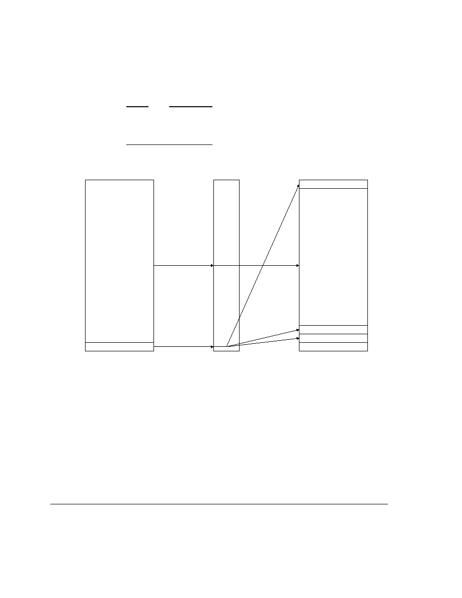
Programmer's Model
3-50
Copyright © 2003 ARM Limited. All rights reserved.
ARM DDI 0244C
Note
If the process ID is zero, as it is on reset, then a flat mapping exists between the integer
unit virtual addresses and the modified virtual addresses used by the caches and the
MMU.
Figure 3-24 FCSE address mapping
4GB
VA from
ARM10 processor
32MB
0MB
VA > 32M
4GB
Process ID No 127
0MB
32MB
64MB
MVA to
caches and MMU
Process ID No 1
Process ID No 2
VA < 32M and
process ID = 1-127
FCSE

Programmer's Model
ARM DDI 0244C
Copyright © 2003 ARM Limited. All rights reserved.
3-51
Writing to the FCSE Process ID Register enables a fast context switch. The contents of
the caches and TLBs do not have to be invalidated after a fast context switch because
they still hold valid address tags. As Example 3-2 shows, from two to six instructions
can be fetched with the old process identifier after the MCR that writes to the process
ID.
Example 3-2 Changing the process ID and performing a fast context switch
{procID = 0}
MOV r0, #1
; Fetched with procID = 0
MCR p15, 0, r0, c13, c0, 0
; Fetched with procID = 0
A0
(any instruction)
; Fetched with procID = 0/1
A1
(any instruction)
; Fetched with procID = 0/1
A2
(any instruction)
; Fetched with procID = 0/1
A3
(any instruction)
; Fetched with procID = 0/1
A4(any instruction)
; Fetched with procID = 0/1
A5
(any instruction)
; Fetched with procID = 0/1
A6
(any instruction)
; Fetched with procID = 1
Note
Do not place any predictable branches or return instructions until at least the seventh
instruction after a process ID change. Before the seventh instruction, the branch target
is fetched from the old process ID, causing Unpredictable behavior.
Fast context switching is an MMU-only feature. Disabling the MMU by clearing the M
bit in the CP15 c1 Control Register or by tying the MMUnMPU pin LOW disables
FCSE address translation. Accesses of the FCSE Process ID Register when using the
MPU (MMUnMPU = 0) take the Undefined instruction trap.

Programmer's Model
3-52
Copyright © 2003 ARM Limited. All rights reserved.
ARM DDI 0244C
3.4.24
CP15 c13 Context ID Register
The read/write Context ID Register holds the current context of the program.
You can access the Context ID Register when using the MMU or the MPU
(MMUnMPU = 1 or 0) with the instructions in Table 3-46.
Figure 3-25 shows the bit field of the Context ID Register.
Figure 3-25 Context ID Register
The reset state of the Context ID Register is Undefined.
3.4.25
CP15 c14 Reserved
CP15 c14 accesses take the Undefined exception trap.
Table 3-46 Context ID Register instructions
Instruction
Operation
MRC p15, 0, Rd, c13, c0, 1
Read Context ID Register
MCR p15, 0, Rd, c13, c0, 1
Write Context ID Register
31
0
Context ID
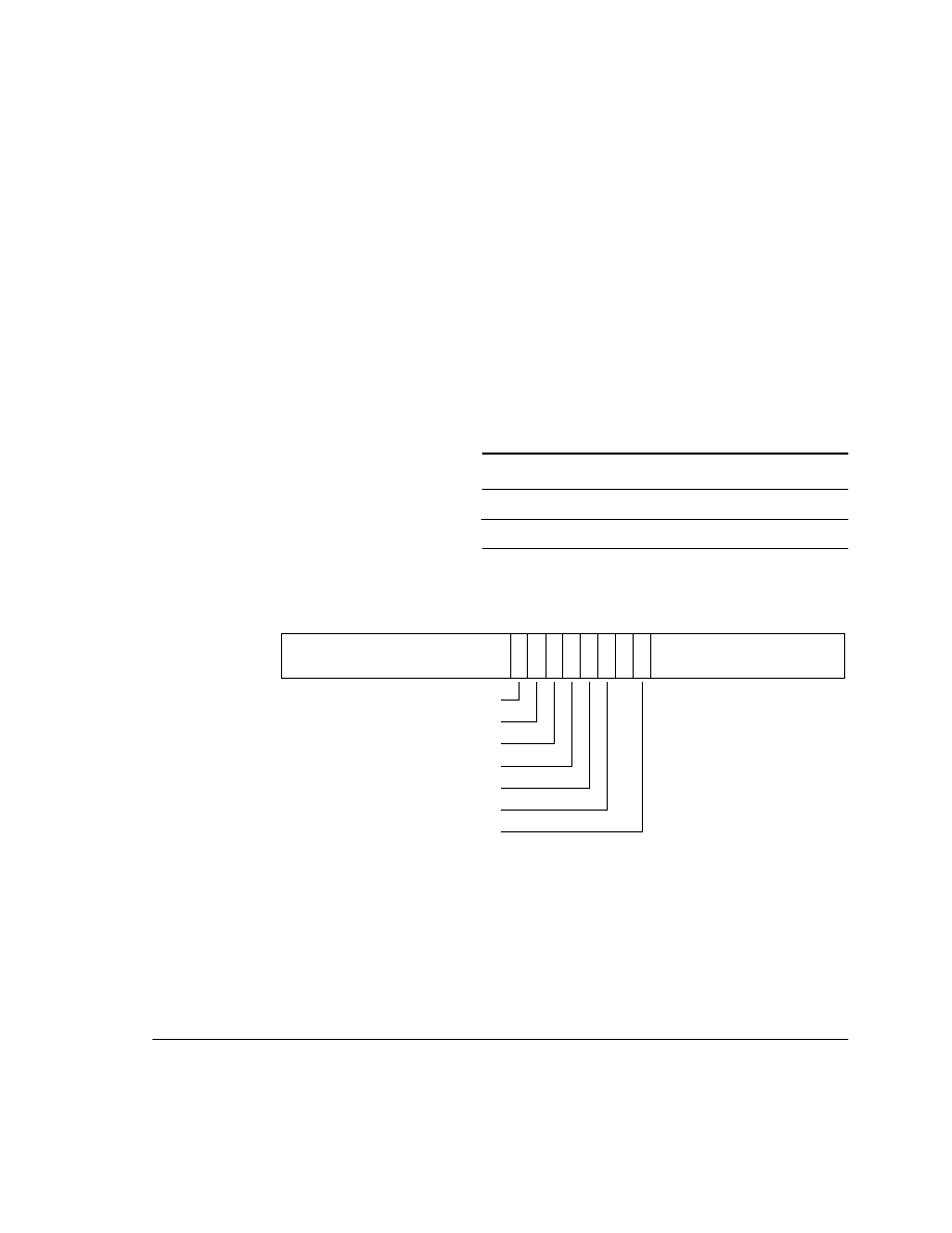
Programmer's Model
ARM DDI 0244C
Copyright © 2003 ARM Limited. All rights reserved.
3-53
3.4.26
CP15 c15 Debug Override Register
CP15 c15 is reserved for device-specific test and debug operations. Software written for
device-specific CP15 c15 operations is unlikely to be either backward or forward
compatible. Most of the CP15 c15 registers are for ARM-internal validation and debug
purposes.
The read/write Debug Override Register contains fields to modify the default behavior
of the ARM1026EJ-S processor.
You can access the Debug Override Register when using the MMU or the MPU
(MMUnMPU = 1 or 0) with the instructions in Table 3-47.
Figure 3-26 shows the Debug Override Register bit fields.
Figure 3-26 Debug Override Register
Table 3-47 Debug Override Register instructions
Instruction
Operation
MRC p15, 0, Rd, c15, c0, 0
Read Debug Override Register
MCR p15, 0, Rd, c15, c0, 0
Write Debug Override Register
31
16 15
12 11
0
19
17
18
13
14
10
SBZ
ADTM
MDDEB
AITM
DNCP
SBZ
FNCNB
IMA
SBZ
W

Programmer's Model
3-54
Copyright © 2003 ARM Limited. All rights reserved.
ARM DDI 0244C
Table 3-48 describes the bit fields of the Debug Override Register.
Caution
The registers that follow are CP15 c15 debug and test registers. They are reserved for
ARM internal use. The following write is not allowed and is potentially catastrophic:
MCR p15, 0, Rd, c15, c0, 1
Table 3-48 Encoding of the Debug Override Register
Bit
Name
Definition
Reset state
[31:19]
-
Should Be Zero.
Zeros
[18]
ADTM
Abort on data TLB miss:
1 = Data Abort enabled on data TLB misses
0 = Data Abort disabled on data TLB misses.
0
[17]
AITM
Abort on instruction TLB miss:
1 = Data Abort enabled on instruction TLB misses
0 = Data Abort disabled on instruction TLB misses.
0
[16]
DNCP
Disable NC instruction prefetching:
1 = NC instruction prefetching disabled
0 = NC instruction prefetching enabled.
0
[15]
-
Should Be Zero.
0
[14]
FNCNB
Force NCB store to be NCNB:
1 = NCB stores treated as nonbufferable
0 = NCB stores are bufferable.
FNCNB overrides setting in MMU page tables and Memory Region
Remap Register.
0
[13]
MDDEB
MMU disabled, DCache enabled behavior:
1 = If MMU disabled and DCache enabled, data accesses are WT.
0 = Normal operation. If MMU disabled, all data accesses are NCNB.
0
[12]
W
Pending write buffer enable:
1 = pending write buffer enabled
0 = pending write buffer disabled.
1
[11]
IMA
Imprecise abort enable:
1 = imprecise abort enabled
0 = imprecise abort disabled.
1
[10:0]
-
Should Be Zero.
Zeros

Programmer's Model
ARM DDI 0244C
Copyright © 2003 ARM Limited. All rights reserved.
3-55
3.4.27
CP15 c15 Prefetch Unit Debug Override Register
The read/write Prefetch Unit Debug Override Register controls the prediction
capabilities of the prefetch unit.
You can access the Prefetch Unit Debug Override Register when using the MMU or the
MPU (MMUnMPU = 1 or 0) with the instructions in Table 3-49.
Figure 3-27 shows the bit fields of the Prefetch Unit Debug Override Register.
Note
The reset value of the Prefetch Unit Override Register is configured for maximum
performance. Changing the value in this register can decrease performance.
Figure 3-27 Prefetch Unit Debug Override Register
Caution
Writing to the Prefetch Unit Debug Override Register after enabling branch prediction
can cause Unpredictable processor behavior.
Table 3-49 Prefetch Unit Debug Override Register instructions
Instruction
Operation
MRC p15, 0, Rd, c15, c0, 2
Read Prefetch Unit Debug Override Register
MCR p15, 0, Rd, c15, c0, 2
Write Prefetch Unit Debug Override Register
0
SBZ
1
EBP
RTK
31
2

Programmer's Model
3-56
Copyright © 2003 ARM Limited. All rights reserved.
ARM DDI 0244C
Table 3-50 describes the bit fields of the Prefetch Unit Debug Override Register.
3.4.28
CP15 c15 Debug and Test Address Register
The read/write Debug and Test Address Register is for the MMU test operations
described in CP15 c15 MMU test operations on page 3-60. It is also useful as a 32-bit
scratch register for validation purposes.
You can access the Debug and Test Address Register when using the MMU or the MPU
(MMUnMPU = 1 or 0) with the instructions in Table 3-51.
Figure 3-28 shows the bit field of the Debug and Test Address Register.
Figure 3-28 Debug and Test Address Register
The reset state of the Debug and Test Address Register is Undefined.
Table 3-50 Encoding of the Prefetch Unit Override Register
Bit
Name
Definition
Reset state
[31:2]
-
Should Be Zero.
Zeros
[1]
EBP
Enhanced branch prediction enable bit:
1 = enabled
0 = disabled.
1
[0]
RTK
Return stack enable bit:
1 = enabled
0 = disabled.
1
Table 3-51 Debug and Test Address Register instructions
Instruction
Operation
MRC p15, 0, Rd, c15, c1, 0
Read Debug and Test Address Register
MCR p15, 0, Rd, c15, c1, 0
Write Debug and Test Address Register
31
0
Debug and test address

Programmer's Model
ARM DDI 0244C
Copyright © 2003 ARM Limited. All rights reserved.
3-57
3.4.29
CP15 c15 Memory Region Remap Register
The read/write Memory Region Remap Register overrides the setting specified in either
the MMU page tables or the MPU region attributes, and the default behaviors if neither
the MMU nor the MPU is enabled.
The Memory Region Register has four fields for remapping instruction-side memory
regions and four fields for remapping data-side memory regions.
You can access the Memory Region Remap Register when using the MMU or the MPU
(MMUnMPU = 1 or 0) with the instructions in Table 3-52.
Figure 3-29 shows the bit fields of the Memory Region Remap Register.
Figure 3-29 Memory Region Remap Register
Table 3-52 Memory Region Remap Register instructions
Instruction
Operation
MRC p15, 0, Rd, c15, c2, 0
Read Memory Region Remap Register
MCR p15, 0, Rd, c15, c2, 0
Write Memory Region Remap Register
15
12 11
8 7
4 3
0
SBZ
13
14
9
10
DNCB
5
6
1
2
DNCNB
DWT
DWB
INCNB
INCB
IWT
IWB
31
16

Programmer's Model
3-58
Copyright © 2003 ARM Limited. All rights reserved.
ARM DDI 0244C
Table 3-53 describes the bit fields of the Memory Region Remap Register.
Table 3-54 shows the encoding of each of the remap fields.
Table 3-53 Encoding of the Memory Region Remap Register
Bit
Name
Definition
Reset state
[31:16]
-
Should Be Zero
0x0000
[15:14]
IWB
Remap select bits for instruction-side write-back region
b11
[13:12]
IWT
Remap select bits for instruction-side write-through region
b10
[11:10]
INCB
Remap select bits for instruction-side noncachable bufferable region
b01
[9:8]
INCNB
Remap select bits for instruction-side noncachable nonbufferable region
b00
[7:6]
DWB
Remap select bits for data-side write-back region
b11
[5:4]
DWT
Remap select bits for data-side write-through region
b10
[3:2]
DNCB
Remap select bits for data-side noncachable bufferable region
b01
[1:0]
DNCNB
Remap select bits for data-side noncachable nonbufferable region
b00
Table 3-54 Encoding of the remap fields
Remap field
b00 = noncachable nonbufferable
b01 = noncachable bufferable
b10 = write-through
b11 = write-back
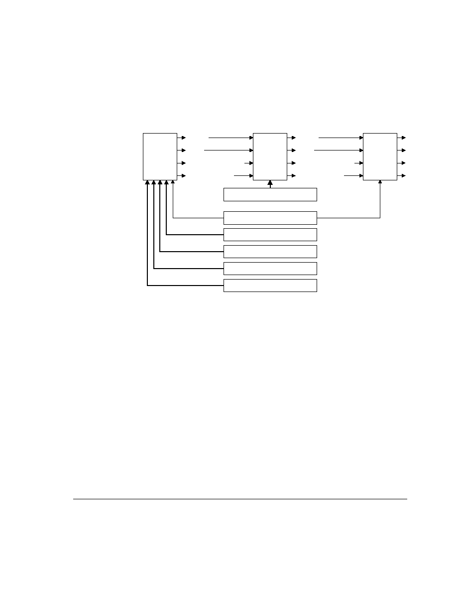
Programmer's Model
ARM DDI 0244C
Copyright © 2003 ARM Limited. All rights reserved.
3-59
Figure 3-30 shows the flow and precedence of CP15 c15 control bits in resolving a the
cachable and bufferable attributes of a memory reference.
Figure 3-30 Memory region attribute resolution
MMU
or
MPU
Memory
region
remapping
NCNB
NCB
CNB (write-through)
CB (write-back)
NCNB
NCB
CNB (write-through)
CB (write-back)
Force
NCB store
to be
NCNB
MDDEB bit:
MMU/MPU
disabled,
DCache enabled
Memory Region Remap Register
Debug Override Register
Page table descriptor
FNCB bit:
Force NCB store
to be NCNB
C and B bits
Cn bits
Cn bits
Bn bits
ICache Configuration Register
DCache Configuration Register
Write Buffer Control Register

Programmer's Model
3-60
Copyright © 2003 ARM Limited. All rights reserved.
ARM DDI 0244C
3.4.30
CP15 c15 MMU test operations
The MMU test operations support accessing TLB structures in the MMU and are used
in conjunction with the Debug and Test Address Register.
You can perform the MMU test operations only when using the MMU
(MMUnMPU = 1) with the instructions in Table 3-55.
Inserting or reading entries in the main TLB
Use this procedure to access entries in the main TLB:
1.
Use the following Debug and Test Address Register instruction to access a main
TLB entry:
MCR p15, 0, Rd, c15, c1, 0 ; select TLB entry
The Rd register selects the main TLB entry as Figure 3-31 shows.
Figure 3-31 Rd format for selecting main TLB entry
Table 3-55 MMU test operation instructions
Instruction
Operation
MRC P15, 4/5, Rd, c15, c2, 0
MCR P15, 4/5, Rd, c15, c3, 0
Read tag in main TLB entry
Write tag in main TLB entry
MRC P15, 4/5, Rd, c15, c4, 0
MCR P15, 4/5, Rd, c15, c5, 0
Read PA and access permission data in main TLB entry
Write PA and access permission data data in main TLB entry
MCR P15, 4/5, Rd, c15, c7, 0
Transfer main TLB entry into RAM
MRC P15, 4/5, Rd, c15, c2, 1
MCR P15, 4/5, Rd, c15, c3, 1
Read tag in lockdown TLB entry
Write tag in lockdown TLB entry
MRC P15, 4/5, Rd, c15, c4, 1
MCR P15, 4/5, Rd, c15, c5, 1
Read PA and access permission data in lockdown TLB entry
Write PA and access permission data in lockdown TLB entry
MCR P15, 4/5, Rd, c15, c7, 1
Transfer lockdown TLB entry into RAM
31
Way
Indexed entry
SBZ
SBZ
14
10
0
9
15
30

Programmer's Model
ARM DDI 0244C
Copyright © 2003 ARM Limited. All rights reserved.
3-61
Table 3-56 describes the Rd register entry-select bit fields.
2.
Use the following MMU test operation instructions to access the MVA tag:
MRC p15, 4/5, Rd, c15, c2, 0 ; read tag in main TLB
MCR p15, 4/5, Rd, c15, c3, 0 ; write tag in main TLB
The Rd register contains the read or write data as Figure 3-32 shows.
Figure 3-32 Rd format for accessing MVA tag of main or lockdown TLB entry
Table 3-56 Encoding of the main TLB entry-select bit fields
Bit
Name
Definition
[31]
Way
Way select:
1 = way 1
0 = way 0.
[30:15]
-
Should Be Zero.
[14:10]
Indexed entry
Indexed entry in mail TLB.
[9:0]
-
Should Be Zero.
0
MVA tag
SBZ
Size of
entry
V
4
1
9
5
10
31

Programmer's Model
3-62
Copyright © 2003 ARM Limited. All rights reserved.
ARM DDI 0244C
Table 3-57 describes the MVA tag access bit fields in the Rd register.
3.
Use the following MMU Test Register instructions to access the PA and access
permission data:
MRC p15, 4/5, Rd, c15, c4, 0 ; read PA and access permission data
MCR p15, 4/5, Rd, c15, c5, 0 ; write PA and access permission data
The Rd register contains the read or write data as Figure 3-33 shows.
Figure 3-33 Rd format for accessing PA and AP data of main or lockdown TLB entry
Table 3-57 Encoding of the TLB MVA tag bit fields
Bit
Name
Definition
[31:10]
MVA tag
Modified virtual address.
[9:5]
-
Should Be Zero.
[4:1]
Size of entry
Size of entry:
b1011 = 1MB section
b0111 = 64KB page
b0101 = 16KB subpage of 64KB page
b0011 = 4KB page
b0001 = 1KB page or 1KB subpage of 4KB page.
[0]
V
Valid bit.
4 3
0
PA
9
Domain
select
5
6
SBZ
1
2
C
AP
[1:0]
B
31
10

Programmer's Model
ARM DDI 0244C
Copyright © 2003 ARM Limited. All rights reserved.
3-63
Table 3-58 describes the PA and access permission bit fields in the Rd register.
4.
Use the following instruction to complete a write to an entry:
MCR p15, 4/5, Rd, c15, c7, 0 ; transfer main storage into RAM
Table 3-58 Encoding of the TLB entry PA and AP bit fields
Bit
Name
Definition
[31:10]
PA
Physical address.
[9:6]
Domain select
Domain select:
b0000 = D0
b0001 = D1
.
.
.
b1110 = D14
b1111 = D15.
[5:4]
-
Should Be Zero.
[3:2]
AP
Access permission:
b00 = No access.
b01 = Privileged, read/write. User, no access.
b10 = Privileged, read/write. User read-only.
b11 = Privileged, read/write. User, read/write.
[1]
C
Cachable bit.
[0]
B
Bufferable bit.

Programmer's Model
3-64
Copyright © 2003 ARM Limited. All rights reserved.
ARM DDI 0244C
Inserting or reading entries in the lockdown TLB
Use this procedure to access entries in the lockdown TLB:
1.
Use the following Debug and Test Address Register instruction to access a
lockdown TLB entry:
MCR p15, 0, Rd, c15, c1, 0
The Rd register selects the lockdown TLB entry as Figure 3-34 shows.
Figure 3-34 Rd format for selecting lockdown TLB entry
Table 3-59 describes the entry-select bit fields in the Rd register.
2.
Use the following MMU Test Register instructions to access the MVA tag:
MRC p15, 4, Rd, c15, c2, 1 ; read lockdown TLB
MCR p15, 4, Rd, c15, c3, 1 ; write lockdown TLB
See Figure 3-32 on page 3-61 for read or write data in the Rd register.
3.
Use the following MMU Test Register instructions to read or write the PA and
access permission data:
MRC p15, 4, Rd, c15, c4, 1 ; read PA and access permission data
MCR p15, 4, Rd, c15, c5, 1 ; write PA and access permission data
See Figure 3-33 on page 3-62 for the read or write data in the Rd register.
4.
Use the following instruction to complete a write to an entry:
MCR p15, 4, Rd, c15, c7, 1 ; transfer lockdown storage into RAM
SBZ
28
26
SBZ
Indexed
entry
31
29
0
25
Table 3-59 Encoding of the lockdown TLB entry-select bit fields
Bit
Name
Definition
[31:29]
-
Should Be Zero
[28:26]
Indexed entry
Indexed entry in lockdown TLB
[25:0]
-
Should Be Zero

Programmer's Model
ARM DDI 0244C
Copyright © 2003 ARM Limited. All rights reserved.
3-65
3.4.31
CP15 c15 Cache Debug Control Register
The read/write Cache Debug Control Register can force a specific cache behavior
required for testing.
You can access the Cache Debug Control Register when using the MMU or the MPU
(MMUnMPU 1 or 0) with the instructions in Table 3-60.
Figure 3-35 shows the bit fields of the Cache Debug Control Register.
Figure 3-35 Cache Debug Control Register
Table 3-60 Cache Debug Control Register instructions
Instruction
Operation
MRC p15, 7, Rd, c15, c0, 0
Read Cache Debug Control Register
MCR p15, 7, Rd, c15, c0, 0
Write Cache Debug Control Register
0
SBZ
DDL
1
2
DIL
DWB
31
3

Programmer's Model
3-66
Copyright © 2003 ARM Limited. All rights reserved.
ARM DDI 0244C
Table 3-61 describes the Cache Debug Control Register bit fields.
Setting the DWB bit forces the DCache to treat all cachable accesses as though they
were in a write-through region. The DWB bit overrides the settings in the:
∑
MMU page tables
∑
MPU Cache Configuration Register
∑
Write Buffer Control Register
∑
Memory Region Remap Register.
Dirty cache lines remain dirty while the DWB bit is set unless they are written back in
a write-back eviction after a linefill or in a clean operation. Lines that are clean are not
marked as dirty if they are updated while the DWB bit is set. This functionality enables
a debugger to download code or data to external memory without having to clean part
or all of the DCache to ensure that the code or data being downloaded has been written
to external memory.
Note
If the DWB bit is set, and a write is made to a dirty cache line, then both the cache line
and external memory are updated with the write data. Other entries in the cache line still
have to be written back to main memory to achieve coherency.
Setting the DDL and DIL bits prevents the cache from updating when performing a
linefill on a miss. A linefill is performed on a cache miss, reading eight words from
external memory, but the cache is not updated with the linefill data. The memory region
mapping is unchanged. This functionality is required for debug so that the
Table 3-61 Encoding of the Cache Debug Control Register
Bit
Name
Definition
Reset state
[31:3]
-
Should Be Zero.
Zeros
[2]
DWB
Disable write-back (force write-through):
1 = write-back disabled
0 = write-back enabled.
0
[1]
DIL
Disable ICache linefills:
1 = disable ICache linefills
0 = enable ICache linefills.
0
[0]
DDL
Disable DCache linefills:
1 = disable DCache linefills
0 = enable DCache linefills.
0

Programmer's Model
ARM DDI 0244C
Copyright © 2003 ARM Limited. All rights reserved.
3-67
ARM1026EJ-S memory image can be examined in a noninvasive manner. Cache hits
from a cachable region read data words from the cache, and cache misses from a
cachable region read words directly from memory.
3.4.32
CP15 c15 MMU Debug Control Register
The read/write MMU Debug Control Register forces TLB behavior to enable
noninvasive testing.
You can use the MMU Debug Control Register to enable TLB and microTLB entries to
be preserved during debug. For debug to be noninvasive, bits [5:0] must be b111111
before changing any other CP15 registers or issuing any load or store. If main TLB
loading is disabled, page table walks still take place, but the resultant data is forwarded
around the TLB.
It might be necessary to temporarily change the contents of a page table entry to
facilitate debug operations. Disabling main TLB matches using bit 6 or 7 enables the
modified contents of the page table to be used for an access without having to invalidate
any entries in the main TLB.
You can access the MMU Debug Control Register only when using the MMU
(MMUnMPU = 1) with the instructions in Table 3-62.
Table 3-62 MMU Debug Control Register instructions
Instruction
Operation
MRC p15, 7, Rd, c15, c1, 0
Read MMU Debug Control Register
MCR p15, 7, Rd, c15, c1, 0
Write MMU Debug Control Register
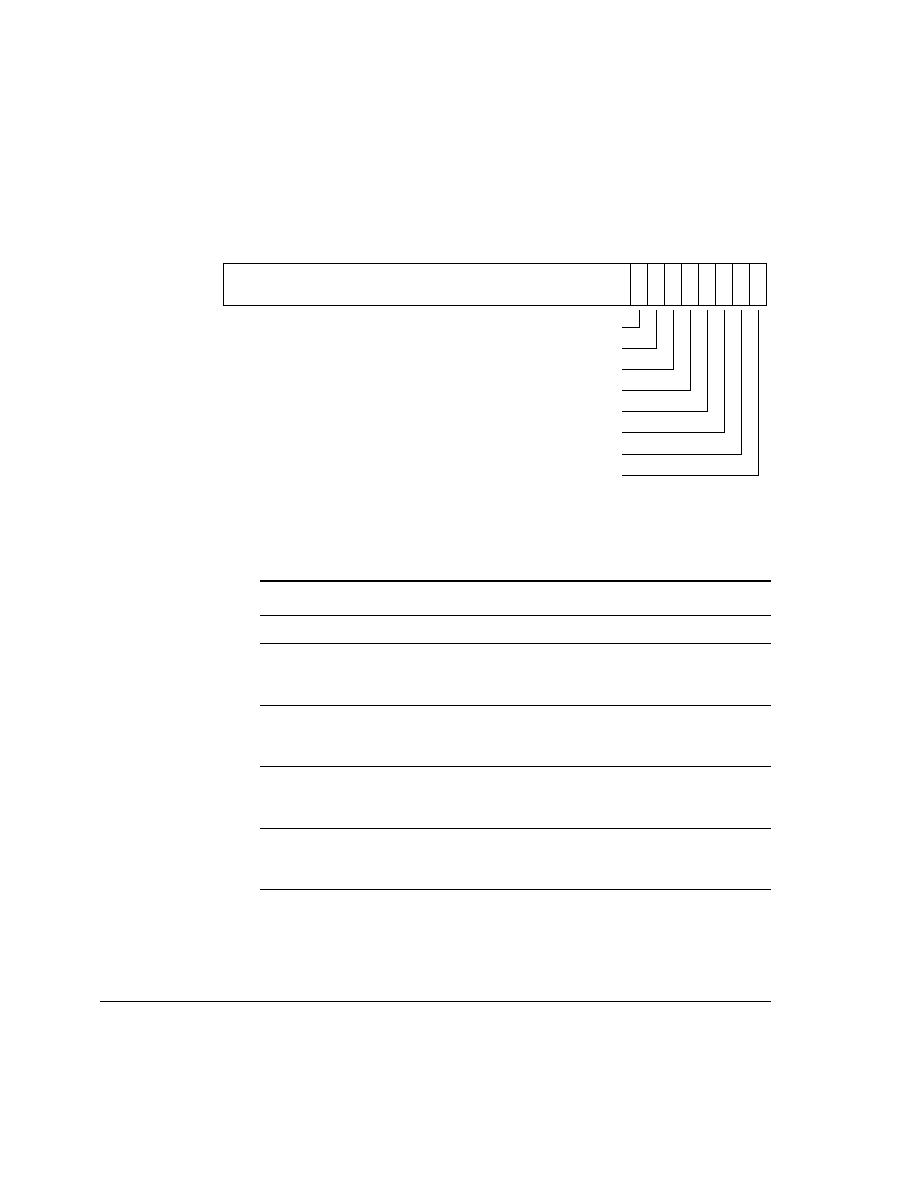
Programmer's Model
3-68
Copyright © 2003 ARM Limited. All rights reserved.
ARM DDI 0244C
Figure 3-36 shows the bit fields of the MMU Debug Control Register.
Figure 3-36 MMU Debug Control Register
Table 3-63 describes the bit fields of the MMU Debug Control Register.
6
3 2
0
SBZ
DMTMD
4
5
DMTLI
DDUTM
1
DIUTL
DMTLD
DIUTM
DMTMI
DDUTL
7
31
8
Table 3-63 Encoding of the MMU Debug Control Register
Bit
Name
Definition
Reset state
[31:0]
-
Should Be Zero.
0x000000
[7]
DMTMI
Disable main TLB matching for instruction fetches:
1 = disable
0 = enable.
0
[6]
DMTMD
Disable main TLB matching for data accesses:
1 = disable
0 = enable.
0
[5]
DMTLI
Disable main TLB load due to instruction miss:
1 = disable
0 = enable.
0
[4]
DMTLD
Disable main TLB load due to data miss:
1 = disable
0 = enable.
0
[3]
DIUTM
Disable instruction microTLB matching:
1 = disable
0 = enable.
0

Programmer's Model
ARM DDI 0244C
Copyright © 2003 ARM Limited. All rights reserved.
3-69
[2]
DDUTM
Disable data microTLB matching:
1 = disable
0 = enable.
0
[1]
DIUTL
Disable instruction microTLB load:
1 = disable
0 = enable.
0
[0]
DDUTL
Disable data microTLB load:
1 = disable
0 = enable.
0
Table 3-63 Encoding of the MMU Debug Control Register (continued)
Bit
Name
Definition
Reset state

Programmer's Model
3-70
Copyright © 2003 ARM Limited. All rights reserved.
ARM DDI 0244C
3.5
CP15 instruction summary
Table 3-64 is a quick reference to the CP15 instructions.
Table 3-64 CP15 instruction summary
Instruction
Operation
Reference
MRC p15, 0, Rd, c0, c0, {0, 3-7}
MRC p15, 0, Rd, c0, c0, 1
MRC p15, 0, Rd, c0, c0, 2
Read Device ID Register.
Read Cache Type Register.
Read TCM Status Register.
Page 3-10
Page 3-11
Page 3-13
MRC p15, 0, Rd, c1, c0, 0
MCR p15, 0, Rd, c1, c0, 0
MRC p15, 0, Rd, c1, c0, 1
Read Control Register.
Write Control Register.
Read Auxiliary Control Register.
Page 3-14
Page 3-14
Page 3-19
MRC p15, 0, Rd, c2, c0, 0
MCR p15, 0, Rd, c2, c0, 0
MRC p15, 0, Rd, c2, c0, 0
MCR p15, 0, Rd, c2, c0, 0
MRC p15, 0, Rd, c2, c0, 1
MCR p15, 0, Rd, c2, c0, 1
Read Translation Table Base Register when using MMU.
Write Translation Table Base Register when using MMU.
Read DCache Configuration Register when using MPU.
Write DCache Configuration Register when using MPU.
Read ICache Configuration Register when using MPU.
Write ICache Configuration Register when using MPU.
Page 3-20
Page 3-20
Page 3-21
Page 3-21
Page 3-21
Page 3-21
MRC p15, 0, Rd, c3, c0, 0
MCR p15, 0, Rd, c3, c0, 0
MRC p15, 0, Rd, c3, c0, 0
MCR p15, 0, Rd, c3, c0, 0
Read Domain Access Control Register when using MMU.
Write Domain Access Control Register when using MMU.
Read Write Buffer Control Register when using MPU.
Write Write Buffer Control Register when using MPU.
Page 3-23
Page 3-23
Page 3-25
Page 3-25
MRC p15, 0, Rd, c5, c0, 0
MCR p15, 0, Rd, c5, c0, 0
MCR p15, 0, Rd, c5, c0, 4
MCR p15, 0, Rd, c5, c0, 4
MRC p15, 0, Rd, c5, c0, 1
MCR p15, 0, Rd, c5, c0, 1
MRC p15, 0, Rd, c5, c0, 5
MRC p15, 0, Rd, c5, c0, 5
MRC p15, 0, Rd, c5, c0, 2
MCR p15, 0, Rd, c5, c0, 2
MRC p15, 0, Rd, c5, c0, 3
MCR p15, 0, Rd, c5, c0, 3
MRC p15, 0, Rd, c5, c0, 0
MCR p15, 0, Rd, c5, c0, 0
MRC p15, 0, Rd, c5, c0, 1
MCR p15, 0, Rd, c5, c0, 1
Read Data Fault Status Register when using MMU.
Write Data Fault Status Register when using MMU.
Read Data Fault Status Register when using MPU.
Write Data Fault Status Register when using MPU.
Read Instruction Fault Status Register when using MMU.
Write Instruction Fault Status Register when using MMU.
Read Instruction Fault Status Register when using MPU.
Write Instruction Fault Status Register when using MPU.
Read Data Extended Access Permission Register when using MPU.
Write Data Extended Access Permission Register when using MPU.
Read Instruction Extended Access Permission Register when using MPU.
Write Instruction Extended Access Permission Register when using MPU.
Read Data Standard Access Permission Register when using MPU.
Write Data Standard Access Permission Register when using MPU.
Read Instruction Standard Access Permission Register when using MPU.
Write Instruction Standard Access Permission Register when using MPU.
Page 3-26
Page 3-26
Page 3-26
Page 3-26
Page 3-26
Page 3-26
Page 3-26
Page 3-26
Page 3-29
Page 3-29
Page 3-29
Page 3-29
Page 3-31
Page 3-31
Page 3-31
Page 3-31

Programmer's Model
ARM DDI 0244C
Copyright © 2003 ARM Limited. All rights reserved.
3-71
MRC p15, 0, Rd, c6, c0, 0
MCR p15, 0, Rd, c6, c0, 0
MRC p15, 0, Rd, c6, c0, 4
MCR p15, 0, Rd, c6, c0, 4
MRC p15, 0, Rd, c6, c0, 1
MCR p15, 0, Rd, c6, c0, 1
MRC p15, 0, Rd, c6, c0, 5
MCR p15, 0, Rd, c6, c0, 5
MRC p15, 0, Rd, c6, c{0-7}, 0
MCR p15, 0, Rd, c6, c{0-7}, 0
Read Data Fault Address Register when using MMU.
Write Data Fault Address Register when using MMU.
Read Data Fault Address Register when using MPU.
Write Data Fault Address Register when using MPU.
Read Instruction Fault Address Register when using MMU.
Write Instruction Fault Address Register when using MMU.
Read Instruction Fault Address Register when using MPU.
Write Instruction Fault Address Register when using MPU.
Read Protection Region Register when using MPU.
Write Protection Region Register when using MPU.
Page 3-33
Page 3-33
Page 3-33
Page 3-33
Page 3-33
Page 3-33
Page 3-33
Page 3-33
Page 3-34
Page 3-34
MCR p15, 0, Rd, c7, c5, 0
MCR p15, 0, Rd, c7, c5, 1
MCR p15, 0, Rd, c7, c5, 2
MCR p15, 0, Rd, c7, c6, 0
MCR p15, 0, Rd, c7, c6, 1
MCR p15, 0, Rd, c7, c6, 2
MCR p15, 0, Rd, c7, c7, 0
MCR p15, 0, Rd, c7, c10, 1
MCR p15, 0, Rd, c7, c10, 2
MCR p15, 0, Rd, c7, c14, 1
MCR p15, 0, Rd, c7, c14, 2
MRC p15, 0, R15, c7, c10, 3
MRC p15, 0, R15, c7, c14, 3
MCR p15, 0, Rd, c7, c0, 4
MCR p15, 0, Rd, c15, c8, 2
MCR p15, 0, Rd, c7, c10, 4
MCR p15, 0, Rd, c7, c13, 1
Invalidate entire ICache.
Invalidate ICache line, MVA format.
Invalidate ICache line, set/way format.
Invalidate entire DCache. Invalidates clean and dirty data.
Invalidate DCache line, MVA format. Invalidates clean and dirty data.
Invalidate DCache line, set/way format. Invalidates clean and dirty data.
Invalidate entire DCache and ICache. Invalidates clean and dirty data.
Clean DCache line, MVA format.
Clean DCache line, set/way format.
Clean and invalidate DCache line, MVA format.
Clean and invalidate DCache line, set/way format.
Test and clean DCache.
Test, clean, and invalidate DCache.
Wait for interrupt.
Drain pending write buffer.
Prefetch ICache line, MVA format.
Page 3-36
Page 3-36
Page 3-36
Page 3-36
Page 3-36
Page 3-36
Page 3-36
Page 3-36
Page 3-36
Page 3-36
Page 3-36
Page 3-36
Page 3-36
Page 3-36
Page 3-36
Page 3-36
MCR p15, 0, Rd, c8, c7, 0
MCR p15, 0, Rd, c8, c5, 0
MCR p15, 0, Rd, c8, c6, 0
MCR p15, 0, Rd, c8, c7, 1
MCR p15, 0, Rd, c8, c5, 1
MCR p15, 0, Rd, c8, c6, 1
Invalidate all unlocked TLB entries when using MMU.
Invalidate all unlocked TLB entries when using MMU.
Invalidate all unlocked TLB entries when using MMU.
Invalidate single TLB entry, MVA format when using MMU.
Invalidate single TLB entry, MVA format when using MMU.
Invalidate single TLB entry, MVA format when using MMU.
Page 3-40
Page 3-40
Page 3-40
Page 3-40
Page 3-40
Page 3-40
MRC p15, 0, Rd, c9, c0, 0
MCR p15, 0, Rd, c9, c0, 0
MRC p15, 0, Rd, c9, c0, 1
MCR p15, 0, Rd, c9, c0, 1
Read DCache Lockdown Register.
Write DCache Lockdown Register.
Read ICache Lockdown Register.
Write ICache Lockdown Register.
Page 3-41
Page 3-41
Page 3-41
Page 3-41
Table 3-64 CP15 instruction summary (continued)
Instruction
Operation
Reference

Programmer's Model
3-72
Copyright © 2003 ARM Limited. All rights reserved.
ARM DDI 0244C
MRC p15, 0, Rd, c9, c1, 0
MCR p15, 0, Rd, c9, c1, 0
MRC p15, 0, Rd, c9, c1, 1
MCR p15, 0, Rd, c9, c1, 1
Read DTCM Region Register.
Write DTCM Region Register.
Read ITCM Region Register.
Write ITCM Region Register.
Page 3-44
Page 3-44
Page 3-44
Page 3-44
MRC p15, 0, Rd, c10, c0, 0
MCR p15, 0, Rd, c10, c0, 0
Read TLB Lockdown Register when using MMU.
Write TLB Lockdown Register when using MMU.
Page 3-46
Page 3-46
MRC p15, 0, Rd, c13, c0, 0
MCR p15, 0, Rd, c13, c0, 0
MRC p15, 0, Rd, c13, c0, 1
MCR p15, 0, Rd, c13, c0, 1
Read FCSE Process ID Register when using MMU.
Write FCSE Process ID Register when using MMU.
Read Context ID Register.
Write Context ID Register.
Page 3-49
Page 3-49
Page 3-52
Page 3-52
MRC p15, 0, Rd, c15, c0, 0
MCR p15, 0, Rd, c15, c0, 0
MRC p15, 0, Rd, c15, c0, 2
MCR p15, 0, Rd, c15, c0, 2
MRC p15, 0, Rd, c15, c1, 0
MCR p15, 0, Rd, c15, c1, 0
MRC p15, 0, Rd, c15, c2, 0
MCR p15, 0, Rd, c15, c2, 0
MRC p15, 4/5, Rd, c15, c2, 0
MCR p15, 4/5, Rd, c15, c3, 0
MRC p15, 4/5, Rd, c15, c4, 0
MCR p15, 4/5, Rd, c15, c5, 0
MCR p15, 4/5, Rd, c15, c7, 0
MRC p15, 4/5, Rd, c15, c2, 1
MCR p15, 4/5, Rd, c15, c3, 1
MRC p15, 4/5, Rd, c15, c4, 1
MCR p15, 4/5, Rd, c15, c5, 1
MCR p15, 4/5, Rd, c15, c7, 1
MRC p15, 7, Rd, c15, c0, 0
MCR p15, 7, Rd, c15, c0, 0
MRC p15, 7, Rd, c15, c1, 0
MCR p15, 7, Rd, c15, c1, 0
Read Debug Override Register.
Write Debug Override Register.
Read Prefetch Unit Debug Override Register.
Write Prefetch Unit Debug Override Register.
Read Debug and Test Address Register.
Write Debug and Test Address Register.
Read Memory Region Remap Register.
Write Memory Region Remap Register.
Read tag in main TLB entry.
Write tag in main TLB entry.
Read PA and access permission data in main TLB entry.
Write PA and access permission data data in main TLB entry.
Transfer main TLB entry into RAM.
Read tag in lockdown TLB entry.
Write tag in lockdown TLB entry.
Read PA and access permission data in lockdown TLB entry.
Write PA and access permission data in lockdown TLB entry.
Transfer lockdown TLB entry into RAM.
Read Cache Debug Control Register.
Write Cache Debug Control Register.
Read MMU Debug Control Register.
Write MMU Debug Control Register.
Page 3-53
Page 3-53
Page 3-55
Page 3-55
Page 3-56
Page 3-56
Page 3-57
Page 3-57
Page 3-60
Page 3-60
Page 3-60
Page 3-60
Page 3-60
Page 3-60
Page 3-60
Page 3-60
Page 3-60
Page 3-60
Page 3-65
Page 3-65
Page 3-67
Page 3-67
Table 3-64 CP15 instruction summary (continued)
Instruction
Operation
Reference

ARM DDI 0244C
Copyright © 2003 ARM Limited. All rights reserved.
4-1
Chapter 4
Clocking and Reset Timing
This chapter describes the relationship between the processor clock, the AHB clock,
and the DBGTAP test clock. It also describes the two ARM1026EJ-S reset signals. It
contains the following sections:
∑
About clock and reset signals on page 4-2
∑
Clock interfaces on page 4-3
∑
Reset on page 4-4.

Clocking and Reset Timing
4-2
Copyright © 2003 ARM Limited. All rights reserved.
ARM DDI 0244C
4.1
About clock and reset signals
CLK is the single global processor clock signal. It drives:
∑
the ARM10EJ-S integer unit
∑
the data and instruction AHB interfaces
∑
the JTAG DBGTAP state machine and logic.
All processor outputs change on the rising edge of CLK, and all inputs are sampled on
the rising edge. CLK can be stretched in either phase.
The overall clocking scheme for the ARM1026EJ-S processor is as follows:
∑
HCLK and CLK must have coincident rising edges
∑
CLK can run at higher frequencies than HCLK if it is an integer multiple of
HCLK
∑
the integer unit, caches, MMUs, and any coprocessors run at CLK speed
∑
the AHB interface runs at HCLK speed, where HCLK = CLK/(1, 2, 3, 4, ...) or
HCLK:CLK = N:1 (N = 1, 2, 3, 4, ...).
Figure 4-1 shows how HCLK is derived from CLK. In this example, the HCLK:CLK
ratio is 4:1.
Figure 4-1 HCLK derivation
The ARM1026EJ-S reset signal, HRESETn, resets all logic except DBGTAP logic.
DBGnTRST is the DBGTAP reset signal.
HCLKEN
CLK
HCLK

Clocking and Reset Timing
ARM DDI 0244C
Copyright © 2003 ARM Limited. All rights reserved.
4-3
4.2
Clock interfaces
The AHB clock enable signals, HCLKENI and HCLKEND, and the DBGTAP clock
enable signal, DBGTCKEN, must be integer multiples of the processor clock, CLK.
4.2.1
AHB clock interface
The synthesizable AHB design restricts AHB operation frequency to be an integer
multiple of CLK. HCLKENI and HCLKEND are the independent clock enable
signals for the instruction and data AHB interfaces. To support multilayer AHB
operation, the AHB the clock enable signals can be different integer multiples of CLK.
4.2.2
DBGTAP clock interface
The synthesizable DBGTAP design restricts the frequency of the test clock, TCK, to an
integer multiple of CLK. The DBGTAP clock enable, DBGTCKEN, must also be an
integer multiple of CLK.
Figure 4-2 shows how TCK is derived from CLK. In this example, the TCK:CLK
ratio is 4:1.
Figure 4-2 TCK derivation
DBGTCKEN
CLK
TCK

Clocking and Reset Timing
4-4
Copyright © 2003 ARM Limited. All rights reserved.
ARM DDI 0244C
4.3
Reset
There are two ARM1026EJ-S reset inputs:
HRESETn Controls all non-JTAG DBGTAP logic. HRESETn must be asserted for
a minimum of eight CLK cycles as Figure 4-3 shows. After HRESETn
deassertion, the processor begins fetching instructions after 20 cycles,
including the deassertion cycle.
Figure 4-3 HRESETn assertion
DBGnTRST Resets DBGTAP logic. You can hold the processor in reset while
removing the DBGTAP logic reset to program the ARM1026EJ-S debug
hardware.
HRESETn
CLK
8 cycles minimum

ARM DDI 0244C
Copyright © 2003 ARM Limited. All rights reserved.
5-1
Chapter 5
Prefetch Unit
This chapter describes how the prefetch unit fetches instructions to feed to the integer
unit and coprocessors, and how it locates branches in the instruction stream for
predicting potential changes in sequential instruction issue. It also describes the SWI
functions useful for flushing the prefetch buffer. It contains the following sections:
∑
About the prefetch unit on page 5-2
∑
Branch prediction activity on page 5-3
∑
Branch instruction cycle summary on page 5-6
∑
Instruction memory barriers on page 5-8.

Prefetch Unit
5-2
Copyright © 2003 ARM Limited. All rights reserved.
ARM DDI 0244C
5.1
About the prefetch unit
The prefetch unit is responsible for fetching instructions from the memory system as
required by the integer unit and coprocessors. The prefetch unit fetches instructions at
up to twice the rate that the integer unit requires them, and the prefetch buffer holds up
to four instructions. The prefetch buffer enables the prefetch unit to:
∑
detect branches several instructions ahead of the currently issuing instruction
∑
predict branches that are likely to be taken
∑
predict subroutine calls
∑
predict leaf subroutine returns
∑
remove those branches that are not likely to be taken.
The bus from the memory system to the prefetch unit is 64 bits wide. It can supply two
ARM instruction words from a doubleword-aligned address every clock cycle.
Branch prediction enables the prefetch unit to provide the branch target instruction to
the integer unit earlier than if no prediction mechanism is used. Branch prediction
increases processor performance by minimizing the cycle time of branch instructions.
When the prefetch unit predicts a branch as taken, it calculates the target address and
fetches instructions from the new address. Depending on how full the prefetch buffer is
at the time the prediction is made, the predicted branch can be reduced to three, two,
one, or zero cycles. When the prefetch unit predicts a branch as not taken, it removes
the branch from the instruction stream passed to the integer unit. It still calculates the
target address of the branch in case the prediction is incorrect. The prediction
mechanism is static. It uses no history information. Conditional forward branches are
predicted as not taken and conditional backward branches are predicted as taken.
The prefetch unit performs branch prediction only when the Z bit is set in the CP15 c1
Control Register.
The prefetch unit also contains a one-entry return stack. Predicted subroutine calls push
the return address into a buffer within the prefetch unit. Subroutines that do not call
other subroutines are called leaf functions. These subroutines can use the BX LR
instruction to return to the caller. Legacy code may also use a MOV PC, LR instruction
where ARM and Thumb state switching is not necessary.

Prefetch Unit
ARM DDI 0244C
Copyright © 2003 ARM Limited. All rights reserved.
5-3
5.2
Branch prediction activity
The prefetch unit predicts all conditional branches.
When the prefetch unit predicts a branch as taken, it speculatively prefetches from the
target address. In speculative prefetching, all cache hits result in an instruction fetched
into the prefetch buffer. Cache misses and noncachable accesses in speculative
prefetching do not initiate a linefill from memory until the integer unit first resolves the
flags and the prediction is confirmed.
5.2.1
Branch folding
Depending on how many instructions are in the prefetch buffer at the time a branch is
predicted, the branch may be completely removed from the instruction stream. This
means:
∑
A branch is pulled from the instruction stream based on a prediction.
∑
The predicted next instruction is substituted in place of this branch.
∑
No empty instruction issue slots results from the process.
Under these circumstances, the branch itself takes zero cycles because it is removed
altogether from the instruction stream to the integer unit. This type of branch removal
that involves direct substitution of another instruction is called branch folding. The
condition codes of the predicted branch are folded onto the predicted next instruction,
and only a single instruction is issued to the integer unit. The condition codes of the
predicted branch are called the branch phantom. The substituted instruction is the
folded instruction.
5.2.2
Flushing the prefetch buffer
The prefetch buffer is flushed in all the following cases:
∑
entry into an exception processing sequence
∑
a load to the PC
∑
an arithmetic manipulation of the PC
∑
execution of an unpredicted branch
∑
detection of an mispredicted branch.
The only changes to sequential instruction fetching that do not automatically flush the
prefetch buffer are a predicted taken branch and a predicted return instruction.

Prefetch Unit
5-4
Copyright © 2003 ARM Limited. All rights reserved.
ARM DDI 0244C
5.2.3
Branch penalty
Mispredicted branches and unpredicted taken branches have a four-cycle penalty
(assuming ICache hit). Here penalty means the number of cycles in which no useful
Execute stage pipeline activity can occur due to an instruction flow differing from that
assumed or predicted. Table 5-1 illustrates this penalty for the case of a mispredicted
branch. Cycles 2, 3, 4, and 5 have nothing valid in Execute stage. The activity is similar
for an unpredicted branch that is taken. Unpredicted branches that are not taken
consume their normal Execute stage and have no branch penalty.
5.2.4
Optimization of branch instructions
This is a complete list of the branch optimizations performed by the branch prediction
unit:
∑
ARM and Thumb conditional branches are predicted taken and potentially
reduced to zero cycles if they branch backwards.
∑
ARM and Thumb conditional branches are predicted not taken and potentially
reduced to zero cycles if they branch forward.
∑
ARM and Thumb unconditional branches are predicted taken and potentially
reduced to zero cycles.
∑
ARM unconditional BL and BLX instructions are predicted taken and potentially
reduced to one cycle.
∑
A Thumb BL pair (always unconditional) is predicted taken and potentially
reduced to one cycle. The pair of instructions must be consecutive in memory for
them to be predicted.
Table 5-1 Penalty for a mispredicted branch
Cycle
Pipeline stage
Activity
1
Execute
Branch phantom, probably with a folded instruction.
Condition code evaluation results in misprediction. All
instructions in earlier pipeline stages are canceled. Folded
instructions are canceled.
2, 3
Fetch
Correct branch target address sent to memory system.
Correct target instruction returned from memory system.
4
Issue
Correct instruction in Issue stage.
5
Decode
Correct instruction in Decode stage.
6
Execute
Correct instruction in Execute stage.

Prefetch Unit
ARM DDI 0244C
Copyright © 2003 ARM Limited. All rights reserved.
5-5
∑
A Thumb BLX pair (always unconditional) is predicted taken and potentially
reduced to one cycle. The pair of instructions must be consecutive in memory for
them to be predicted.
When BL and BLX instructions are predicted, the instruction is changed into a link
instruction and a branch instruction. The link part of the instruction is passed to the
integer unit as a special MOV LR instruction. The branch part is predicted taken.
Branches are not predicted in any of the following cases:
∑
the Z bit in the CP15 c1 Control Register is clear
∑
a Prefetch Abort occurs when fetching the instruction
∑
a breakpoint is set on the instruction address
∑
the processor is in Jazelle state
∑
the branch immediately precedes another predictable branch. For example:
BEQ ERROR
BNE LOOP
Note
In this case, BNE is not predicted.
5.2.5
Return stack
The prefetch unit also contains a one-entry return stack. Predicted subroutine call
instructions (BL and BLX instructions) push the return address and caller ARM/Thumb
state into a buffer within the prefetch unit. The BL and BLX instructions place the
return PC into the Link Register (LR). Subroutine that call other subroutines must save
this register onto a memory stack. Subroutines that do not call other subroutines, called
leaf functions, keep the return address in the link register and use the BX LR instruction
to return to the caller. Legacy code may also use the MOV PC, LR instruction where
ARM and Thumb state interworking is not required. These two instructions are
predicted, with the stored address and mode being the next fetch address. If the
predicted return address does not match the value of LR or the mode does not match,
then a mispredict occurs and the pipeline is flushed.

Prefetch Unit
5-6
Copyright © 2003 ARM Limited. All rights reserved.
ARM DDI 0244C
5.3
Branch instruction cycle summary
The number of cycles taken by the ARM10 processor to execute branch instructions
depends primarily on:
∑
Whether or not the branch is predicted.
∑
Whether or not the predicted branch is correct.
∑
What direction the predicted branch takes, forward or backward.
∑
The number of instructions in the prefetch buffer ahead of the branch at the time
the prediction is made. The prefetch buffer continues to issue instructions while
a predicted branch target instruction is being fetched.
Table 5-2 shows the instruction cycle counts for all ARM and Thumb branches. The
cycle counts are based on ICache hits, because the cycle counts of ICache misses and
noncachable accesses vary widely as a function of system and implementation
characteristics.
Instructions are listed here by their ARM Architecture Reference Manual name. Some
instructions have multiple variations that distinguish unique characteristics among a
common instruction, for example Thumb B(1) and Thumb B(2).
Table 5-2 ARM and Thumb branch instruction cycle counts
Unpredicted
condition code
Predicted correctly
Predicted incorrectly
Instruction
Fail
Pass
Backward/taken Forward/not
taken Backward/taken Forward/not taken
ARM instructions
B uncond
a
5
0-3
0-3
b
b
B cond
1
5
0-3
0
c
5
5
BL uncond
a
5
1-3
d, e
1-3
d, e
b
b
BL cond
2
5
e
e
e
e
BLX(1) uncond
a
5
1-3
d, e
1-3
d, e
b
b
BLX(2) uncond
a
5
f
f
f
f
BLX(2) cond
2
5
f
f
f
f
BX uncond
a
5
f
f
f
f

Prefetch Unit
ARM DDI 0244C
Copyright © 2003 ARM Limited. All rights reserved.
5-7
BX cond
2
5
f
f
f
f
BX LR
-
-
1
g
1
g
6
6
MOV PC,LR
-
-
1
g
1
g
6
6
Thumb instructions
B(1) cond
1
5
0-3
0
b
5
5
B(2) uncond
a
5
0-3
0-3
b
b
BL uncond
a
7
h
1-3
d
1-3
d, e
b
b
BLX(1) uncond
a
7
h
1-3
d
1-3
d, e
b
b
BLX(2) uncond
a
5
f
f
f
f
BX uncond
a
5
f
f
f
f
BX LR
-
-
1
g
1
g
6
6
MOV PC,LR
-
-
1
g
1
g
6
6
a. Unconditional branches (either unconditional by instruction definition or by using cond code AL, always) cannot fail
condition codes.
b. Unconditional branches, when predicted, can never be mispredicted.
c. All forward branches are predicted only when prefetch buffer contains at least two instructions, the branch being predicted
and its preceding instruction.
d. ARM and Thumb BL and BLX instructions can never be reduced to 0 cycles by prediction because the link operation
necessarily consumes a cycle.
e. ARM and Thumb BL and BLX instructions are only predicted if unconditional, in which case they are predicted taken
irrespective of direction (guaranteed to be correct).
f.
ARM and Thumb BX and BLX(2) instructions are not PC-relative. They cannot be predicted except for the special case of
BX LR and MOV PC, LR when used as return instructions.
g. The leaf return instructions are only predicted if unconditional, in which case they are predicted taken irrespective of
direction (guaranteed to be correct).
h. Thumb BL and BLX(1) instructions are encoded as two Thumb instructions. The first of these is a data processing
instruction that puts an immediate value into r14 and then fetches from that address. This second instruction takes five
cycles before the next instruction is in Execute.
Table 5-2 ARM and Thumb branch instruction cycle counts (continued)
Unpredicted
condition code
Predicted correctly
Predicted incorrectly
Instruction
Fail
Pass
Backward/taken Forward/not taken Backward/taken Forward/not taken

Prefetch Unit
5-8
Copyright © 2003 ARM Limited. All rights reserved.
ARM DDI 0244C
5.4
Instruction memory barriers
The prefetch unit performs speculative prefetching of instructions. In some
circumstances it is likely that the prefetch buffer contains out-of-date instructions. In
these circumstances the prefetch buffer must be flushed. An Instruction Memory
Barrier (IMB) sequence provides a means to do this.
You can include processor-specific code in the SWI handler to implement the two IMB
sequences:
IMB
The IMB sequence flushes all information about all instructions.
IMBRange When only a small area of code is altered before being executed, the
IMBRange sequence can efficiently and quickly flush any stored
instruction information from addresses within a small range. By flushing
only the required address range information, the rest of the information
remains to provide improved system performance.
The IMB and IMBRange sequences are implemented as calls to specific SWI numbers.
5.4.1
Generic IMB use
Use SWI functions to provide a well-defined interface between code that is:
∑
independent of the ARM processor implementation on which it is running
∑
specific to the ARM processor implementation on which it is running.
The implementation-independent code is provided with a function that is available on
all processor implementations through the SWI interface, and that can be accessed by
privileged and, where appropriate, nonprivileged (User mode) code.
Using SWIs to implement the IMB instructions means that code that is written now
remains compatible with future ARM processors, even if those processors implement
IMB in different ways. This is achieved by changing the operating system SWI service
routines for each of the IMB SWI numbers that differ from processor to processor.
5.4.2
IMB implementation
Executing the SWI instruction is sufficient to cause IMB operation. Also, both the IMB
and the IMBRange sequences flush all stored information about the instruction stream.
This means that all IMB instructions can be implemented in the operating system by
returning from the IMB/IMBRange service routine and that the service routines can be
exactly the same. The following service routine code can be used:

Prefetch Unit
ARM DDI 0244C
Copyright © 2003 ARM Limited. All rights reserved.
5-9
IMB_SWI_handler
IMBRange_SWI_handler
MOVS PC, R14_svc
; Return to the code after the SWI call
Note
In new code, you are strongly encouraged to use the IMBRange sequence whenever the
changed area of code is small, even if there is no distinction between it and the IMB
sequence. Future ARM processors might implement a faster and more efficient
IMBRange sequence, and code migrated from this ARM processor can benefit when
executed on future ARM processors.
5.4.3
Execution of IMB sequences
This section gives examples that show what should happen during IMB sequences. The
pseudocode in the square brackets shows what should happen in the SWI routine.
Loading code from disk
Code that loads a program from a disk and then branches to the entry point of that
program must use an IMB sequence after loading the program and before executing it:
IMB EQU 0xF00000
.
.
; code that loads program from disk
.
.
SWI IMB
[branch to IMB service routine]
[perform processor-specific operations to execute IMB]
[return to code]
.
MOV PC, entry_point_of_loaded_program
.
.
Running BitBlt code
Compiled BitBlt routines optimize large copy operations by constructing and executing
a copying loop that has been optimized for a particular operation. When writing such a
routine, an IMB is required between the code that constructs the loop and the execution
of the constructed loop:

Prefetch Unit
5-10
Copyright © 2003 ARM Limited. All rights reserved.
ARM DDI 0244C
IMBRange EQU 0xF00001
.
.
; code that constructs loop code
; load R0 with the start address of the constructed loop
; load R1 with the end address of the constructed loop
SWI IMBRange
[branch to IMBRange service routine]
[read registers R0 and R1 to set up address range parameters]
[do processor-specific operations to execute IMBRange within address range]
[return to code]
; start of loop code
.
.
Self-decompressing code
When writing a self-decompressing program, an IMBmust be issued after the routine
that decompresses the bulk of the code and before the decompressed code is to be
executed:
IMB EQU 0xF00000
.
.
; copy and decompress bulk of code
SWI IMB
; start of decompressed code

ARM DDI 0244C
Copyright © 2003 ARM Limited. All rights reserved.
6-1
Chapter 6
Bus Interface
This chapter describes the features of the bus interface not covered in the AMBA
Specification. It contains the following sections:
∑
About the bus interface on page 6-2
∑
Bus transfer characteristics on page 6-3
∑
Bus transfer cycle timing on page 6-8
∑
Topology on page 6-23
∑
Endianness of BIU transfers on page 6-24
∑
64-bit and 32-bit AHB data buses on page 6-25.

Bus Interface
6-2
Copyright © 2003 ARM Limited. All rights reserved.
ARM DDI 0244C
6.1
About the bus interface
The ARM1026EJ-S processor is designed to be used within larger chip designs using
the Advanced Microcontroller Bus Architecture (AMBA). The ARM1026EJ-S
processor uses the AMBA High-performance Bus Lite (AHB-Lite) interface to memory
and peripherals.
To make your design reusable with future revisions of ARM processors, use fully
AMBA-compliant peripherals and interfaces early in your design cycle.
The ARM1026EJ-S processor uses separate AHB bus interfaces for instructions and
data:
∑
Instruction Bus Interface Unit (IBIU)
∑
Data Bus Interface Unit (DBIU).
Separate bus interfaces enhance the ability to fetch and execute instructions in parallel
with a DCache miss. There is no sharing of any AHB signals between the two
interfaces.
The I64n32 and D64n32 pins independently configure the instruction and data
interfaces to widths of 32 or 64 bits respectively.
The ARM1026EJ-S processor has unidirectional inputs, outputs, and control signals
that are always driven. Because the processor is AHB-Lite compliant, it always drives
a valid sequential, nonsequential, or idle AHB transfer.
For a complete description of AMBA, including the AHB bus and the AMBA test
methodology see the AMBA Specification.
The BIU handles the following transfers:
∑
cachable instruction and data read transfers
∑
noncachable instruction and data read transfers
∑
buffered data write transfers
∑
nonbuffered data write transfers
∑
noncachable nonbuffered data swaps
∑
data eviction write transfers
∑
hardware page table walk data read transfers.

Bus Interface
ARM DDI 0244C
Copyright © 2003 ARM Limited. All rights reserved.
6-3
6.2
Bus transfer characteristics
The bus interface handles all data transfers and instruction transfers between the core
clock domain and the AMBA bus clock domain. Any request from the prefetch unit or
the LSU that has to go outside the ARM1026EJ-S processor is handled by the bus
interface in a way that is transparent to the prefetch unit and the LSU.
The types of AMBA bus transfers are:
∑
MMU generated page table walks
∑
noncachable instruction fetches and data loads
∑
nonbuffered data stores
∑
instruction and data linefills
∑
data evictions due to replacement or CP15 operations
∑
buffered data stores
∑
noncachable nonbufferable data swap operations.
Each of the AMBA AHB bus transfers generates a signature. For design flexibility, the
BIU supports 32-bit and 64-bit instruction and data buses. The bus width affects the
signature generated by the BIU.
Table 6-1 on page 6-4 and Table 6-2 on page 6-5 list the types of DBIU and IBIU
transfers and their characteristics.

Bus Interface
6-4
Copyright © 2003 ARM Limited. All rights reserved.
ARM DDI 0244C
Table 6-1 DBIU transfer characteristics
Transfer
Bus
w
i
dth
HADDRD
a
HTRANSD
b
HPROTD
c
HSIZED
HBURSTD
HLOCKD
HWRIT
E
D
Hx
DA
T
A
D
MMU page
table walk
32
[31:2] b00
NS
[c b 1 1]
32
Single
0
0
[31:0]
64
[31:2] b00
NS
[c b 1 1]
32
Single
0
0
[63:0]
Noncachable
load
32
[31:0]
NS
[c b p 1]
8, 16, 32
Single
0
0
[31:0]
32
[31:3] bbb
NS-S
[c b p 1]
32
d
Incr
0
0
[63:0]
64
[31:3] bbb
NS
[c b p 1]
8, 16, 32, 64
Single
0
0
[63:0]
Nonbufferable
store
32
[31:0]
NS
[c b p 1]
8, 16, 32
Incr
0
1
[31:0]
32
[31:3] bbb
NS-S
[c b p 1]
32
d
Incr
0
1
[63:0]
64
[31:3] bbb
NS
[c b p 1]
8, 16, 32, 64
Incr
0
1
[63:0]
Buffered
store
32
[31:2] bb
NS-S-S- . . . -S
[c b p 1]
8, 16, 32
Incr
0
1
[31:0]
64
[31:3] bbb
NS-S-S- . . . -S
[c b p 1]
8, 16, 32, 64
Incr
0
1
[63:0]
Cachable
linefill
32
[31:2] b00
NS-S-S-S-S-S-S-S
[c b p 1]
32
Wrap8
0
0
[31:0]
64
[31:3] b000
NS-S-S-S
[c b p 1]
64
Wrap4
0
0
[63:0]
Eviction/
castout
32
[31:2] b00
NS-S-S-S-S-S-S-S
[c b 1 1]
32
Incr8
0
1
[31:0]
64
[31:3] b000
NS-S-S-S
[c b 1 1]
64
Incr4
0
1
[63:0]
Swap (load)
32
[31:2] b00
NS
[c b p 1]
32
Single
1
0
[31:0]
Swap (store)
32
[31:2] b00
NS
[c b p 1]
32
Single
1
1
[31:0]
Swap (load)
64
[31:2] b00
NS
[c b p 1]
32
Single
1
0
[63:0]
Swap (store)
64
[31:2] b00
NS
[c b p 1]
32
Single
1
1
[63:0]
a. See Transfer size on page 6-6.
b. See Sequential and nonsequential transfers on page 6-6.
c. See BIU protection control on page 6-6.
d. The internal 64-bit request is converted to two 32-bit transfers to match the AHB bus width.

Bus Interface
ARM DDI 0244C
Copyright © 2003 ARM Limited. All rights reserved.
6-5
Table 6-2 lists the IBIU transfer types and their characteristics.
Table 6-2 IBIU transfer characteristics
Transfer
AHB bus
width
HADDRI
a
HTRANSI
b
HPROTI
c
HSIZEI
HBURSTI
HLOCKI
HWRIT
E
I
Hx
DA
T
A
I
d
Noncachable
fetch
e
32
[31:2] bb
NS
[c b p 0]
16, 32
Single
0
0
[31:0]
32
[31:3] bbb
NS-S
[c b p 0]
32
f
Incr
0
0
[63:0]
64
[31:3] bbb
NS
[c b p 0]
16, 32, 64
Single
0
0
[63:0]
Noncachable
fetch
g
32
[31:2] b00
NS-S-S-S-S-S-S-S
[c b p 0]
32
Wrap8
0
0
[31:0]
64
[31:3] b000
NS-S-S-S
[c b p 0]
64
Wrap4
0
0
[63:0]
Cachable
linefill
32
[31:2] b00
NS-S-S-S-S-S-S-S
[c b p 0]
32
Wrap8
0
0
[31:0]
64
[31:3] b000
NS-S-S-S
[c b p 0]
64
Wrap4
0
0
[63:0]
a. See Transfer size on page 6-6.
b. See Sequential and nonsequential transfers on page 6-6.
c. See BIU protection control on page 6-6.
d. See AHB reads on page 6-7.
e. With noncachable prefetching disabled by setting CP15 c15 Debug Override Register bit 16, DNCP.
f.
The internal 64-bit request is converted to two 32-bit transfers to match the AHB bus width.
g. With noncachable prefetching enabled by clearing CP15 c15 Debug Override Register bit 16, DNCP.

Bus Interface
6-6
Copyright © 2003 ARM Limited. All rights reserved.
ARM DDI 0244C
6.2.1
Transfer size
HSIZE[2:0] defines transfer size and determines values of low-order address bits
HADDR[2:0], which appear in the HADDR column of Table 6-1 on page 6-4 and
Table 6-2 on page 6-5 as b, bb, or bbb. An eight-bit transfer does not affect
HADDR[2:0]. A 16-bit transfer forces HADDR[0] to 0. A 32-bit transfer forces
HADDR[1:0] to b00. A 64-bit transfer forces HADDR[2:0] to b000.
6.2.2
Sequential and nonsequential transfers
The HTRANS column in Table 6-1 on page 6-4 and Table 6-2 on page 6-5 shows
whether transfers are sequential (S) or nonsequential (NS). Any burst of four elements
is always an NS-S-S-S transfer. Any burst of eight elements is always an
NS-S-S-S-S-S-S-S transfer. In a DBIU buffered store, the burst can be from one to n
elements, shown as NS-S-S- . . . -S. The n value is the number of sequential data stores
calculated at run-time for all forms of store instructions defined in the ARM
Architectural Reference Manual.
6.2.3
BIU protection control
The four HPROT[3:0] signals indicate the four protection attributes:
∑
cachability
∑
bufferability
∑
accessibility (User or privileged)
∑
transfer type (instruction or data).
For page table walks, the cachability and bufferability attributes (c and b in the HPROT
column of Table 6-1 on page 6-4 and Table 6-2 on page 6-5) reflect the L2C and L2B
bits in the CP15 c2 Translation Table Base Register. For all other AHB accesses using
the MMU, c and b reflect the C and B bits in the level 1 and level 2 descriptors. For
accesses using the MPU, c and b reflect the C and B bits for the protection region. The
p (privileged) attribute reflects the decoding of the mode bits in the CPSR. HPROT[0]
is set for data accesses and cleared for opcode fetches.

Bus Interface
ARM DDI 0244C
Copyright © 2003 ARM Limited. All rights reserved.
6-7
AHB swap operations
The DBIU can perform locked bus transfers only for ARM swap instructions. It begins
the swap operation by asserting HLOCKD and performing a locked nonsequential
read. The DBIU monitors the AHB for an error response to the nonsequential read.
If the nonsequential read returns an AHB error response, the ARM1026EJ-S processor
terminates the swap operation and does not perform the locked nonsequential write. The
locked indicator is deasserted in the cycle following the return of the AHB error
response.
If the nonsequential read does not return an AHB error response, the DBIU keeps
HLOCKD asserted until the ARM1026EJ-S processor performs the nonsequential
write. Until the nonsequential write begins, the DBIU issues idle AHB cycles.
6.2.4
AHB reads
In an AHB read, the memory system must drive HRDATA according to the state of
HADDR[2], which defines the half of the bus that contains valid data. When
HADDR[2] = 0, HRDATA[31:0] contains the valid transfer data. When
HADDR[2] = 1, HRDATA[63:32] contains the valid transfer data. The only exception
to this rule is in 64-bit transfers, in which case HRDATA[63:0] contains valid data.

Bus Interface
6-8
Copyright © 2003 ARM Limited. All rights reserved.
ARM DDI 0244C
6.3
Bus transfer cycle timing
Transfer cycle counts are affected by:
∑
64-bit or 32-bit AHB width.
∑
Transfer size.
∑
AHB wait states.
∑
HCLK-to-CLK frequency ratio.
∑
Proximity of the transfer to other transfers. The cycle count of an isolated transfer
can differ from the cycle count of the same transfer when it occurs in a series of
other transfers. Pipelining of address phase and data phase activity with other
transfers reduces the effective cycle count of each transfer.
∑
Presence of valid TLB and cache entries at the time of the transfer request.
This section contains cycle-count equations and diagrams of common AHB transfers.
The equations represent the effective total number of cycles that the instruction remains
in the Memory stage of the integer core pipeline. The equations apply only to transfers
that are not affected by pipelining with other transfers. In the cycle-count diagrams, the
clock domain indicator G represents the internal clock, CLK, and H represents the AHB
clock, HCLK.
The common AHB transfer cycle counts described are:
∑
Cache linefill cycle count
∑
Cache castout cycle count on page 6-14
∑
Level 1 and level 2 table walk cycle count on page 6-16
∑
NC load and NCNB store cycle count on page 6-19.
6.3.1
Cache linefill cycle count
Clock cycle equations and diagrams for cache linefills are affected by the width of the
AHB interface as shown in:
∑
With a 64-bit AHB interface on page 6-9
∑
With a 32-bit AHB interface on page 6-11.

Bus Interface
ARM DDI 0244C
Copyright © 2003 ARM Limited. All rights reserved.
6-9
With a 64-bit AHB interface
The critical doubleword CLK cycles represent the total number of cycles the transfer
remains in the Memory stage of the integer core pipeline. The total number of critical
doubleword CLK cycles is:
5 + TW + (H
◊ (2 + AC + AM + WS))
The best case, with H = 1 and TW = AC = AM = WS = 0, is 5 + 2H = 7 CLK cycles.
The total number of CLK cycles for linefill completion includes critical doubleword
completion and completion of the linefill on the AHB. The total number of CLK cycles
for completing all words of a linefill is:
5 + TW + (H
◊ (5 + AC + AM + 4 ◊ WS))
The best case, with H = 1 and TW = AC = AM = WS = 0, is 5 + 5H = 10 CLK cycles.
Table 6-3 defines the variables in the cycle-count equations for a cache linefill with a
64-bit AHB interface.
Figure 6-1 on page 6-10 shows the number of CLK and HCLK cycles in a cache
linefill using a 64-bit AHB interface.
Table 6-3 Definition of variables in cache linefills with 64-bit interface
Variable
Definition
TW
Number of table walk cycles (see Figure 6-5 on page 6-18)
H
HCLK:CLK frequency ratio
AC
Number of HCLK cycles, {0, 1, 2}, to synchronization point when CLK couples to
HCLK, depending on when transfer request appears in relation to HCLK rising edge
AM
Number of HCLK cycles, {0, 1, 2, . . .}, for completion of data phase of previous
transfer
WS
Number of HCLK cycles, {0, 1, 2, . . .}, for AHB data phase wait states
Bus Interface
6-10
Copyright © 2003 ARM Limited. All rights reserved.
ARM DDI 0244C
Figure 6-1 Cache linefill cycle count with 64-bit AHB
Table 6-4 defines the symbols used in Figure 6-1.
G
1
H
1+WS
H
1+AM
G+H
1
G
+AC
H
G
1+TW
G
1
EX a
BIU c
ME b
ACKd
DATf
ADRe
2nd doubleword
3rd doubleword
4th doubleword
1st doubleword
CAPg
Critical word
Clock domain
Cycles
ME
WR i
G
1
G
1
G
1
H
1+WS
WR i
ME h
CAPg
f
G
1
G
1
G
1
H
1+WS
WR i
ME h
CAPg
f
G
1
G
1
G
1
H
1+WS
WR i
ME h
CAPg
f
G
1
G
1
G
1
h
DAT
DAT
DAT
Memory stage stalled for linefill critical
doubleword
Table 6-4 Symbols used in linefill cycle counts with 64-bit AHB
Symbol
Definition
a
Issue of request from integer core to memory system
b
Cache lookup, miss determined
c
Cache request to BIU
d
BIU acknowledge cycle
e
AHB address cycle
f
AHB data cycle for doubleword
g
BIU data capture cycle
h
Critical doubleword valid in linefill buffer and in integer core ME pipeline stage
i
Instruction retired in integer core and WR pipeline stage completes
G
Internal clock, CLK
H
AHB clock, HCLK

Bus Interface
ARM DDI 0244C
Copyright © 2003 ARM Limited. All rights reserved.
6-11
With a 32-bit AHB interface
Internally, there is fixed 64-bit interface between caches and the BIU. When the AHB
interface is configured to a 32-bit width, the BIU must accumulate words into
doubleword packets when responding to the cache linefill request.
The critical doubleword CLK cycles represent the total number of cycles the transfer
remains in the Memory stage of the integer core pipeline. The total number of critical
doubleword CLK cycles is:
5 + TW + (H
◊ (3 + AC + AM + 2 ◊ WS))
The best case, with H = 1 and TW = AC = AM = WS = 0, is 5 + 3H = 8 CLK cycles.
The total number of CLK cycles for linefill completion includes critical doubleword
completion and completion of the linefill on the AHB. The total number of CLK cycles
for completing all words of a linefill is:
5 + TW + (H
◊ (9 + AC + AM + 8 ◊ WS))
The best case, with H = 1 and TW = AC = AM = WS = 0, is 5 + 9H = 14 CLK cycles.
Table 6-5 defines the variables in the cycle-count equations for a cache linefill with a
64-bit AHB interface.
Figure 6-2 on page 6-12 shows the number of CLK and HCLK cycles in a cache
linefill using a 32-bit AHB interface.
Table 6-5 Definition of variables in cache linefills with 32-bit interface
Variable
Definition
TW
Number of table walk cycles (see Figure 6-5 on page 6-18)
H
HCLK:CLK frequency ratio
AC
Number of HCLK cycles, {0, 1, 2}, to synchronization point when CLK couples to
HCLK, depending on when transfer request appears in relation to HCLK rising edge
AM
Number of HCLK cycles, {0, 1, 2, . . .}, for completion of data phase of previous
transfer
WS
Number of HCLK cycles, {0, 1, 2, . . .}, for AHB data phase wait states

Bus Interface
6-12
Copyright © 2003 ARM Limited. All rights reserved.
ARM DDI 0244C
Figure 6-2 Cache linefill cycle count with 32-bit AHB
Critical word
Clock domain
Cycles
Memory stage stalled for linefill critical
doubleword
G
1
G
1
G
1
H
1+WS
p CAPq ME r WR s
G
1
G
1
H
1+WS
CAPq ME r WR s
H
1+WS
H
1+WS
CAPh
WR j
ME i
8th
word
G
1
H
1+WS
H
1+AM
G
1+TW
G
1
EX a
BIU c
ME b
ACKd
DATf
ADRe
2nd
word
3rd
word
4th
word
5th
word
6th
word
7th
word
1st
word
G
1
G
1
G
1
G
1
DATg
DAT
DATm
H
1+WS
G
1
G
1
G
1
H
1+WS
DATp CAPq ME r WR s
DATm
H
1+WS
DATp
DATm
G+H
1
G
+AC
H

Bus Interface
ARM DDI 0244C
Copyright © 2003 ARM Limited. All rights reserved.
6-13
Table 6-6 defines the symbols in used in Figure 6-2 on page 6-12.
Table 6-6 Symbols used in linefill cycle counts with a 32-bit AHB
Symbol
Definition
a
Issue of request from integer core to memory system
b
Cache lookup, miss determined
c
Cache request to BIU
d
BIU acknowledge cycle
e
AHB address cycle
f (m)
AHB data cycle for first word in doubleword pair
g (p)
AHB data cycle for second word in doubleword pair
h (q)
BIU data capture cycle
i (r)
Critical doubleword valid in linefill buffer and in integer core ME pipeline stage
j (s)
Load retired in integer core and WR pipeline stage completes
G
Internal clock, CLK
H
AHB clock, HCLK

Bus Interface
6-14
Copyright © 2003 ARM Limited. All rights reserved.
ARM DDI 0244C
6.3.2
Cache castout cycle count
Clock cycle equations and diagrams for cache castouts are affected by the width of the
AHB interface as shown in:
∑
With a 64-bit AHB interface
∑
With a 32-bit AHB interface on page 6-16.
With a 64-bit AHB interface
The number of CLK cycles for completing a castout on the AHB using a 64-bit AHB
interface is:
NR + NA + H
◊ (5 + AC + AM + (4 ◊ WS))
The best case, with NR = 0, NA = H = 1 and AC = AM = WS = 0, is 6 CLK cycles.
Table 6-9 on page 6-17 defines the variables in the cycle-count equations for castouts.
Table 6-7 Definition of variables in castouts
Variable
Definition
NR
Number of CLK cycles , {0}, for cache request to BIU for castout under linefill
NA
Number of CLK cycles to BIU acknowledgement
1 if WS = 0 and H = 1
0 if WS
1 or H 2
H
HCLK:CLK frequency ratio
AC
Number of HCLK cycles, {0, 1, 2}, to synchronization point when CLK couples to HCLK,
depending on when transfer request appears in relation to HCLK rising edge
AM
Number of HCLK cycles, {0, 1, 2, . . .}, for completion of data phase of previous transfer
WS
Number of HCLK cycles, {0, 1, 2, . . .}, for AHB data phase wait states

Bus Interface
ARM DDI 0244C
Copyright © 2003 ARM Limited. All rights reserved.
6-15
Figure 6-3 shows the number of CLK and HCLK cycles in a cache castout using a
64-bit AHB interface.
Figure 6-3 Cache castout cycle count with 64-bit AHB interface
Table 6-8 defines the symbols used in Figure 6-3 and in Figure 6-4 on page 6-16.
G
1
H
1+AM
G
1+TW
Clock domain
Cycles
b
c
d
G
1
Cache linefill
ADR
ME
BIU
ACK
DAT
1
f
a
EX
H
1+WS
. . . DAT
4
f
H
1+WS
H
1+AM
g
G
NR
ADR
BIU
DAT
1
j
H
1+WS
. . . DAT
4
j
H
1+WS
e
i
Cache castout
G+H
1
G
+AC
H
G+H
NA
G
+AC
H
h
ACK
Table 6-8 Symbols used in linefill cycle counts with 64-bit AHB
Symbol
Definition
a
Issue of request from integer core to memory system
b
Cache lookup, miss determined
c
Cache request to BIU for linefill
d
BIU acknowledge cycle for linefill
e
AHB address cycle for linefill
f
AHB data cycle for linefill critical doubleword
g
Cache request to BIU for castout
h
BIU acknowledge cycle for castout
i
AHB address cycle for castout
j
AHB clock cycles for castout
G
Internal clock, CLK
H
AHB clock, HCLK
Bus Interface
6-16
Copyright © 2003 ARM Limited. All rights reserved.
ARM DDI 0244C
With a 32-bit AHB interface
The number of CLK cycles for completing a castout on AHB using a 32-bit AHB
interface is:
1 + H
◊ (9 + AC + AM + (8 ◊ WS))
The best case, with H = 1 and AC = AM = WS = 0, is 10 CLK cycles.
Refer to Table 6-7 on page 6-14 for the definition of the variables for castout
cycle-count equations.
Figure 6-4 shows the number of CLK and HCLK cycles in a cache castout using a
32-bit AHB interface.
Figure 6-4 Cache castout cycle count with 32-bit AHB interface
Refer to Table 6-7 on page 6-14 for the definition of the variables in castout cycle
counts with a 32-bit AHB interface.
6.3.3
Level 1 and level 2 table walk cycle count
The number of CLK cycles that the Memory pipeline stage is stalled during a level 1
and level 2 table walk is:
7 + NM + (H
◊ (2 + AC + AM + WS)) + L2 ◊ (2 +H ◊ (2 + AC + AM + WS))
The best case for only a level 1 table walk (NM = 2 and L2 = 0), with H = 1 and
AC = AM = WS = 0, is 9 + 2H = 11 CLK cycles.
The best case for a level 1 and level 2 table walk (NM = 2 and L2 = 1), with H = 1 and
AC = AM = WS = 0, is 11 + 4H = 15 CLK cycles.
Table 6-9 on page 6-17 defines the variables in the cycle-count equations for level 1 and
level 2 table walks.
G
1
H
1+AM
G
1+TW
Clock domain
Cycles
b
c
d
G
1
Cache linefill
ADR
ME
BIU
ACK
DAT
1
f
a
EX
H
1+WS
. . . DAT
8
f
H
WR
H
1+AM
g
h
G
NR
ADR
BIU
ACK
DAT
1
j
H
1+WS
. . . DAT
8
j
H
1+WS
e
i
Cache castout
. . .
. . .
G+H
1
G
+AC
H
G+H
1
G
+AC
H

Bus Interface
ARM DDI 0244C
Copyright © 2003 ARM Limited. All rights reserved.
6-17
Table 6-9 Definition of variables in level 1 and level 2 table walks
Variable
Definition
NM
Number of lookups, {2, 4, 5, 6, 7, 8} required in main TLB, a function of the number of
valid page sizes and current page size in relation to last main TLB page size accessed
H
HCLK:CLK frequency ratio
AC
Number of HCLK cycles, {0, 1, 2}, to synchronization point when CLK couples to
HCLK, depending on when transfer request appears in relation to HCLK rising edge
AM
Number of HCLK cycles, {0, 1, 2, . . .}, for completion of data phase of previous
transfer
WS
Number of HCLK cycles, {0, 1, 2, . . .}, for AHB data phase wait states
L2
1 if level 1 and level 2 table walk
0 if level 1 table walk only

Bus Interface
6-18
Copyright © 2003 ARM Limited. All rights reserved.
ARM DDI 0244C
Figure 6-5 shows the number of CLK and HCLK cycles in a level 1 and level 2 table
walk.
Figure 6-5 Level 1 and level 2 table walk cycle count
G
1
H
1+WS
H
1+AM
G
1
e
Clock domain
Cycles
G
1
G
1
H
1+WS
G
2
Memory stage stalled for table walk
m
a
b
c
d
G
NM
f
g
h
i
j
H
1+AM
k
l
n
G
2
G
Level 1
descriptor fetch
L1D
ACK
uTLB
calc
EX
uTLB mTLB
L1D
REQ
L1D
ADR
L1D
DAT
L2D
REQ
L2D
ACK
L2D
ADR
L2D
DAT
mTLB
calc
ME
Level 2
descriptor fetch
G+H
1
G
+AC
H
G+H
1
G
+AC
H

Bus Interface
ARM DDI 0244C
Copyright © 2003 ARM Limited. All rights reserved.
6-19
Table 6-10 defines the symbols used in Figure 6-5 on page 6-18.
6.3.4
NC load and NCNB store cycle count
Clock cycle counts for noncachable loads and noncachable, nonbufferable stores are
affected by the width of the AHB interface and by the size of the transfer as shown in:
∑
For a transfer with one data phase on page 6-20
∑
For a transfer with two data phases on page 6-22.
Table 6-10 Symbols used in level 1 and level 2 table walk cycle counts
Symbol
Meaning
a
Issue of load or store request from integer core to memory system
b
uTLB lookup, miss determined
c
Main TLB lookup
d
AHB request for level 1 descriptor
e
BIU acknowledge cycle
f
AHB address cycle for level 1 descriptor
g
AHB data cycle for level 1 descriptor
h
AHB request cycle for level 2 descriptor
i
BIU acknowledge cycle
j
AHB address cycle for level 2 descriptor
k
AHB data cycle for level 2 descriptor
l
Main TLB result calculation
m
uTLB result calculation
n
Memory stage no longer stalled by table walk, and access underway in memory system
G
Internal clock, CLK
H
AHB clock, HCLK

Bus Interface
6-20
Copyright © 2003 ARM Limited. All rights reserved.
ARM DDI 0244C
For a transfer with one data phase
The number of CLK cycles that a noncachable load remains in the Memory stage of the
integer core pipeline is:
4 + (H
◊ (2 + AC + AM + WS))
The best case, with H = 1 and AC = AM = WS = 0, is 4 + 2H = 6 CLK cycles.
The number of CLK cycles that a in a noncachable, nonbufferable store remains in the
Memory stage of the integer core pipeline is:
3 + (H
◊ (2 + AC + AM + WS))
The best case, with H = 1 and AC = AM = WS = 0, is 3 + 2H = 5 CLK cycles.
Table 6-11 defines the variables in the cycle-count equations for noncachable loads and
noncachable, nonbufferable stores with one or two data phases.
Figure 6-6 on page 6-21 shows the number of CLK and HCLK cycles in noncachable
loads and noncachable, nonbufferable stores with a single data phase. A transfer with a
single data phase includes:
∑
a byte, halfword, word, or doubleword transfer on a 64-bit AHB interface
∑
a byte, halfword, or word transfer on a 32-bit AHB interface.
Table 6-11 Definition of variables in NC loads and NCNB stores
Variable
Definition
H
HCLK:CLK frequency ratio
AC
Number of HCLK cycles, {0, 1, 2}, to synchronization point when CLK couples
to HCLK, depending on when transfer request appears in relation to HCLK rising
edge
AM
Number of HCLK cycles, {0, 1, 2, . . .}, for completion of data phase of previous
transfer
WS
Number of HCLK cycles for AHB data phase wait states

Bus Interface
ARM DDI 0244C
Copyright © 2003 ARM Limited. All rights reserved.
6-21
Figure 6-6 Cycle count of NC loads and NCNB stores with one data phase
Table 6-12 defines the symbols used in Figure 6-6.
G
1
G
NC
H
1+WS
G
1
ME stalled for transaction handling and
completion on AHB
a
H
1+AM
b
G
1
EX
ME
c
G
1+TW
BIU
d
G
1
ACK
e
ADR
f
DAT
g
CAP
h
ME
i
WR
Clock domain
Cycles
G+H
1
G
+AC
H
Table 6-12 Symbols used in NC load and NCNB store cycle counts
Symbol
Definition
a
Issue of request from integer core to memory system
b
External transfer queue entry
c
External transfer queue request to BIU
d
BIU acknowledge cycle
e
AHB address cycle
f
AHB data cycle
g
BIU data capture cycle
h
Data valid and transfer complete in integer core Memory pipeline stage
i
Load retired in integer core and Write pipeline stage completes
NC
Number of BIU data capture cycles:
1 if load
0 if store
G
Internal clock, CLK
H
AHB clock, HCLK

Bus Interface
6-22
Copyright © 2003 ARM Limited. All rights reserved.
ARM DDI 0244C
For a transfer with two data phases
Figure 6-7 shows the number of CLK and HCLK cycles in a noncachable load and a
noncachable, nonbufferable store using a 32-bit AHB interface.
The number CLK cycles that a noncachable load remains in the Memory stage of the
integer core pipeline is:
4 + (H
◊ (3 + AC + AM + 2 ◊ WS))
The best case, with H = 1 and AC = AM = WS = 0, is 4 + 3H = 7 CLK cycles.
The number CLK cycles that a noncachable, nonbufferable store remains in the
Memory stage of the integer core pipeline is:
3 + (H
◊ (2 + AC + AM + 2 ◊ WS))
The best case, with H = 1 and AC = AM = WS = 0, is 3 + 3H = 6 CLK cycles.
Refer to Table 6-11 on page 6-20 for the definitions of the variables in the equations for
noncachable loads and noncachable, nonbufferable stores.
Figure 6-7 shows the number of CLK and HCLK cycles in noncachable loads and
noncachable, nonbufferable stores with a double data phase. A transfer with a double
data phase is a doubleword transfer on a 32-bit AHB interface.
Figure 6-7 Cycle count of NC loads and NCNB stores with two data phases
Refer to Table 6-12 on page 6-21 for the definitions of the symbols in used in
Figure 6-7.
G
1
G
NC
H
1+WS
G
1
ME stalled for transaction handling and completion on
AHB
a
H
1+AM
b
G
1
EX
ME
c
G
1+TW
BIU
d
G
1
ACK
e
ADR
f
DAT
g
CAP
h
ME
i
WR
Clock domain
Cycles
H
1+WS
f
DAT
G+H
1
G
+AC
H
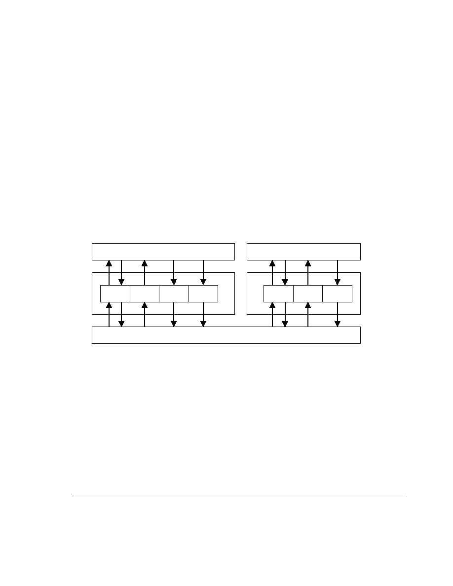
Bus Interface
ARM DDI 0244C
Copyright © 2003 ARM Limited. All rights reserved.
6-23
6.4
Topology
The bus interface consists of two completely separate blocks:
∑
the IBIU handles all instruction fetches and linefills
∑
the DBIU performs all data loads and stores.
The DBIU performs all data page table walks and instruction page table walks for the
MMU. HPROTD[0] marks all page table walk transfers as data transfers.
Figure 6-8 shows the structure of the bus interface. The DBIU is on the left with control,
read, write, and address data path. The IBIU on the right has a read and an address data
path only because no writes ever happen on the instruction side. Both the IBIU and the
DBIU have a similar layer for transferring data or instructions to and from the HCLK
domain and further on to the rest of the AMBA system. The arrows illustrate the flow
of requests and data or instructions.
Figure 6-8 Bus interface block diagram
The DBIU and the IBIU are independent of each other. Because there is no efficient
way of communicating between the data and the instruction side, software must
appropriately handle any self-modifying code.
CLK domain
HCLK domain
Read
datapath
Control
Address
datapath
Address
datapath
Read
datapath
Write
datapath
DBIU
IBIU
DCache, MMU, DExt (write buffer)
ICache, IExt (NC prefetch engine)
AHB
Control
Bus Interface
6-24
Copyright © 2003 ARM Limited. All rights reserved.
ARM DDI 0244C
6.5
Endianness of BIU transfers
The ARM1026EJ-S processor supports both little-endian and big-endian memory
systems. The CFGBIGEND output indicates the current endianness setting of the
processor and reflects the value of the B bit in the CP15 c1 Control Register.
Before changing the B bit, the software must first complete any outstanding load/store
operations and then drain the write buffer. Draining the write buffer forces all buffered
writes onto AHB in the appropriate endianess. Because all instructions fetches are at
least 32-bit transfers, changing the B bit does not affect instruction fetches on the AHB.
In addition to the CFGBIGEND output, the ARM1026EJ-S processor also has byte
lane strobe outputs for both instruction AHB requests and data AHB requests. The byte
lane strobes, HBSTRBI[7:0] and HBSTRBD[7:0], are encoded in little-endian format.
As Figure 6-9 shows, an HBSTRBx[7:0] value of
0x03
indicates halfword 0 in a
little-endian structure and halfword 1 in a big-endian structure. A value of
0x01
indicates
byte 0 in little-endian and byte 3 in big-endian.
Figure 6-9 Endianness of byte lane strobes
HBSTRBx
[7]
[6]
[5]
[4]
[3]
[2]
[1]
[0]
0
0
0
0
0
0
1
1
0
0
0
0
0
0
0
1
0x3
0x1
byte 7
byte 6
byte 5
byte 4
byte 3
byte 2
byte 1
byte 0
halfw ord 3
halfw ord 2
halfw ord 1
halfw ord 0
w ord 1
w ord 0
Little-endian data structure
byte 0
byte 1
byte 2
byte 3
byte 4
byte 5
byte 6
byte 7
halfw ord 0
halfw ord 1
halfw ord 2
halfw ord 3
w ord 0
w ord 1
Big-endian data structure

Bus Interface
ARM DDI 0244C
Copyright © 2003 ARM Limited. All rights reserved.
6-25
6.6
64-bit and 32-bit AHB data buses
The instruction and data AHB interfaces of the ARM1026EJ-S processor can be
statically and independently configured to be 64 bits wide or 32 bits wide. This enables
you to integrate the processor into existing 64-bit or 32-bit AHB systems.
The alignment of the AHB buses is a function of their width. See Figure 6-10 on
page 6-26. If the AHB buses are 32 bits wide, then the both even and odd words appear
on HxDATAD[31:0] only, leaving the HxDATAD[63:32] inputs and outputs either
tied off or unconnected. If the AHB buses are 64 bits wide, then the even words must
always be mapped onto HxDATAD[31:0], and the odd words must always be mapped
onto HxDATAD[63:32].
Note
In Figure 6-10 on page 6-26, the multiplexors represent hardware in the design
necessary to accommodate 32-bit/64-bit AHB configurability.
For 64-bit systems, the multiplexor select inputs are fixed so that HRDATAD[63:32]
is always passed to internal read data [63:32], and internal write data [31:0] is always
passed to HWDATAD[31:0].

Bus Interface
6-26
Copyright © 2003 ARM Limited. All rights reserved.
ARM DDI 0244C
Figure 6-10 AHB bus alignment
Internal write data bits [31:0]
Internal write data bits [63:32]
HWDATA[63:32] odd
HWDATA[31:0] even
Internal read data bits [63:32]
Internal read data bits [31:0]
HRDATA[63:32] odd
HRDATA[31:0] even
64-bit AHB bus alignment
32-bit AHB bus alignment
Internal write data bits [31:0]
Internal write data bits [63:32]
HWDATA[63:32] unconnected
HWDATA[31:0] even/odd
Internal read data bits [63:32]
Internal read data bits [31:0]
HRDATA[63:32]
HRDATA[31:0] even/odd

ARM DDI 0244C
Copyright © 2003 ARM Limited. All rights reserved.
7-1
Chapter 7
Coprocessor Interface
This chapter contains information about the coprocessor interface. It contains the
following sections:
∑
About the coprocessor interface on page 7-2
∑
Coprocessor interface signals on page 7-3
∑
Design considerations on page 7-5
∑
Parallel execution on page 7-8
∑
Rules for the interface on page 7-9
∑
Pipeline signal assertion on page 7-10
∑
Instruction issue on page 7-11
∑
Hold signals on page 7-21
∑
Instruction cancelation on page 7-40
∑
Bounced instructions on page 7-47
∑
Data buses on page 7-53.

Coprocessor Interface
7-2
Copyright © 2003 ARM Limited. All rights reserved.
ARM DDI 0244C
7.1
About the coprocessor interface
The coprocessor interface enables you to attach multiple coprocessors (CPs) to the
ARM1026EJ-S processor. To limit the number of connections required by the interface,
each CP tracks the progress of instructions in the ARM1026EJ-S pipeline.
To enable optimum performance from CPs, the ARM1026EJ-S processor issues CP
instructions as early as possible. This means that the instructions are issued
speculatively, and they can be canceled later in the pipeline if, for example, an
exception or branch misprediction occurs. As a result, CPs must be able to cancel
instructions in late stages of the ARM1026EJ-S pipeline.
Simple CPs track the ARM1026EJ-S pipeline only until they are certain that a given
instruction is not going to be canceled. At this point the CP starts to execute the
instruction. More complex CPs make extensive use of the early issue of the instruction.
At certain points in the pipeline, a CP sends back signals to the ARM1026EJ-S
processor. These can indicate that the CP requires more time to execute or to indicate
that the undefined instruction exception must be taken.
7.1.1
CP pipeline
The CP pipeline runs one cycle behind the ARM1026EJ-S pipeline. This enables
pipeline holds from the ARM1026EJ-S processor to be registered before they are sent
to the CPs. Figure 7-1 shows the ARM1026EJ-S and CP pipeline stages.
Figure 7-1 ARM1026EJ-S and CP pipeline stages
CP pipeline
ARM10 pipeline
Write
Memory
Execute
Decode
Issue
Fetch
Write
Memory
Execute
Decode
Issue
Fetch

Coprocessor Interface
ARM DDI 0244C
Copyright © 2003 ARM Limited. All rights reserved.
7-3
7.2
Coprocessor interface signals
This section divides the CP signals according to function:
∑
ARM1026EJ-S instruction progression signals
∑
ARM1026EJ-S instruction cancelation signals
∑
CPBOUNCEE on page 7-4
∑
Busy-waiting instruction on page 7-4
∑
CP data buses on page 7-4
∑
CP control signals on page 7-4.
7.2.1
ARM1026EJ-S instruction progression signals
The signals that indicate instruction progression are:
CPINSTRV
Valid CP instruction in ARM1026EJ-S Issue stage.
CPVALIDD
Valid CP instruction in ARM1026EJ-S Decode stage.
ASTOPCPD
ARM1026EJ-S processor stalled in Decode stage in previous
cycle.
ASTOPCPE
ARM1026EJ-S processor stalled in Execute stage in previous
cycle.
LSHOLDCPE
ARM1026EJ-S LSU stalled in Execute stage in previous cycle.
LSHOLDCPM
ARM1026EJ-S LSU stalled in Memory stage in previous cycle.
7.2.2
ARM1026EJ-S instruction cancelation signals
Two signals indicate ARM1026EJ-S instruction cancelation:
ACANCELCP
Cancels only the instruction that was in ARM1026EJ-S Execute stage in
the previous cycle.
AFLUSHCP
Cancels all the instructions back from the one that was in ARM1026EJ-S
Execute stage in the previous cycle. AFLUSHCP overrides STOP and
VALID signals from the ARM1026EJ-S processor and causes BUSY
signals to be deasserted in the following cycle.

Coprocessor Interface
7-4
Copyright © 2003 ARM Limited. All rights reserved.
ARM DDI 0244C
7.2.3
CPBOUNCEE
The signal that indicates whether a CP can execute an instruction is:
CPBOUNCEE
Takes the undefined instruction trap for the instruction that is in
the ARM1026EJ-S Execute stage.
7.2.4
Busy-waiting instruction
The signal that indicates whether a CP requires more time to process an instruction is:
CPBUSYE Busy-wait (stall) the ARM1026EJ-S Execute stage.
Note
The ARM1026EJ-S processor has CPBUSYD1 and CPBUSYD2 inputs. These are
reserved for future expansion. Tie these off to a logic 0.
7.2.5
CP data buses
There are two 64-bit CP data buses:
∑
STCMRCDATA carries data from a CP to the ARM1026EJ-S processor
∑
LDCMRCDATA carries data from the ARM1026EJ-S processor to a CP.
7.2.6
CP control signals
CPLSLEN, CPLSSWP, and CPLSDBL are signals driven by a CP to the
ARM1026EJ-S processor on load/store CP instructions. They carry additional
information about:
∑
the length of the transfer
∑
if upper and lower half of the data bus must be swapped before being written
∑
if the load/store request is for double word data.
Note
The ARM1026EJ-S processor has a CPABORT output that is reserved for future
expansion. Leave CPABORT unconnected.

Coprocessor Interface
ARM DDI 0244C
Copyright © 2003 ARM Limited. All rights reserved.
7-5
7.3
Design considerations
This section outlines CP interface design considerations for single and multiple CPs.
7.3.1
Input and output timing
Almost all the signals on both sides of the interface must be driven straight out of
registers. This is necessary because there is very little timing slack in the interface.
There is very little timing slack because as few cycles as practical have been used to
process a given CP instruction. This enables very high performance CPs to be built. If
performance is not an issue, then timing across the interface can be greatly simplified
by stalling all CP instructions in situations where timing is an issue.
7.3.2
ARM1026EJ-S processor inputs and outputs
Outputs driven from the ARM1026EJ-S processor go to all the CPs in the system. The
inputs to the ARM1026EJ-S processor from all the CPs are ANDed or ORed together
before they are used. As a result, the ARM1026EJ-S processor cannot determine which
CP is driving its inputs. Figure 7-2 on page 7-6 shows CPBUSYE and CPBOUNCEE
as examples of ARM1026EJ-S coprocessor input gating. The problem of multiple CPs
driving a signal at the same time is avoided, because there can only be one CP
instruction in each ARM1026EJ-S pipeline stage. So only one CP can own the
instruction in that stage and can drive the associated signals.

Coprocessor Interface
7-6
Copyright © 2003 ARM Limited. All rights reserved.
ARM DDI 0244C
Figure 7-2 ARM1026EJ-S coprocessor inputs
The ARM1026EJ-S processor has control inputs for up to two external coprocessors.
The two sets of inputs are differentiated by appending a 1 or a 2 to the signal name.
Inputs that are not used must be tied off. By convention, single-coprocessor systems
use the 1 inputs and tie off the 2 inputs. Adding more than two external coprocessors
requires external gating.
Any system with more than one external coprocessor requires external gating for the
STCMRCDATA bus inputs to the ARM1026EJ-S processor. This is to avoid the
necessity of routing 64-bit buses to the ARM1026EJ-S processor.
CPBOUNCEE1
Three
coprocessors
ARM1026EJ-S processor
CPBOUNCEE
internal
CPBUSYE
internal
CPBUSYE1
CPBUSYE3
CPBUSYE2
CPBOUNCEE2
CPBOUNCEE3
One
coprocessor
CPBOUNCEE
internal
CPBOUNCEE1
V
DD
CPBUSYE
internal
CPBUSYE1
V
SS
Two
coprocessors
CPBOUNCEE
internal
CPBOUNCEE1
CPBOUNCEE2
CPBUSYE
internal
CPBUSYE1
CPBUSYE2
ARM1026EJ-S processor
ARM1026EJ-S processor

Coprocessor Interface
ARM DDI 0244C
Copyright © 2003 ARM Limited. All rights reserved.
7-7
7.3.3
CP input loadings
When a CP does not own the instruction associated with an ANDed signal it must drive
the signal HIGH. When a CP does not own the instruction associated with an ORed
signal it must drive the signal LOW. The ARM1026EJ-S processor drives instruction,
data, and control outputs to all CPs, so the loading on these signals might become an
issue in multiple-CP systems. Keep CP input loadings low, and buffer these signals
where appropriate.
7.3.4
Combining outputs from multiple CPs
Outputs from all the CPs are ANDed or ORed together before they are used in the
ARM1026EJ-S processor. The AND and OR gates can be placed in the level of the
design instantiating the ARM1026EJ-S processor and the CPs. To aid timing for control
signals, there is one level of ANDing and ORing inside the ARM1026EJ-S processor.
The ARM1026EJ-S processor implements the ANDing and ORing necessary on the
control signals of up to two external CPs. For more than two CPs, external gates must
be used to OR the hold signals from the external CP into the existing inputs.
Although the ARM1026EJ-S processor implements the necessary inputs for only two
external CPs, this does not have to be the limiting factor in a system with three or more
CPs. In such a system, the wire delays from the farthest CP probably balance the time
required to AND or OR the control signal from the closer CPs. For systems with more
than one CP, external gates are always required for the CP STCMRCDATA bus. These
are not included in the ARM1026EJ-S design as this would have forced the entire bus
to be duplicated on the interface. Also, the freedom to place the gates anywhere in the
top-level design helps with floor planning of the bus route.
7.3.5
CP ID number
The ARM1026EJ-S processor issues all CP instructions to all the CPs. Each CP in the
system has a unique, hardwired ID number from 0 to 15. Every CP instruction includes
a CP number.
Only the CP whose ID number corresponds to the number in the CP instruction can
accept the instruction. To accept an instruction, a CP must pull CPBOUNCEE LOW
at the right time. If no CP pulls CPBOUNCEE LOW, then the instruction is bounced.
That is, the ARM1026EJ-S processor takes the undefined instruction trap. This enables
error trapping or software emulation of a CP not present in the system.
A CP does not have to accept an instruction even if its ID corresponds to the CP number
in the instruction. This is used in cases where some of the CP instructions are handled
in hardware and some are handled in software.

Coprocessor Interface
7-8
Copyright © 2003 ARM Limited. All rights reserved.
ARM DDI 0244C
7.4
Parallel execution
Initially, instructions progress along the ARM1026EJ-S pipeline and CP pipeline in
lockstep. A CP instruction moves along the ARM1026EJ-S pipeline as a single-cycle
instruction. When the first cycle of the instruction traverses the entire length of the
ARM1026EJ-S pipeline, one of three things can occur:
∑
If the instruction is complete in the CP pipeline, then it is retired in both pipelines.
∑
If the CP instruction is a multicycle data processing type, then the ARM1026EJ-S
processor and CP pipelines are decoupled. The instruction continues to iterate in
the CP but is retired in the ARM1026EJ-S pipeline. When the pipelines are
decoupled, the ARM1026EJ-S processor cannot cancel the instruction, and the
CP must complete the instruction. While the CP is working, the ARM1026EJ-S
processor continues to execute the following instruction stream and issues any CP
instructions it hits. The CP can hold up any following CP instructions as
necessary. The ARM1026EJ-S processor is not explicitly signaled when the CP
completes the instruction. The CP usually holds up any following instruction that
is dependent on a prior instruction.
∑
If the CP instruction is a multicycle load or store type, then the ARM1026EJ-S
ALU pipeline and CP pipelines are decoupled, but the ARM1026EJ-S LSU
pipeline and CP pipeline remain coupled. The instruction continues to iterate in
the CP and the ARM1026EJ-S LSU pipelines but is retired in the ARM1026EJ-S
ALU pipeline. When the ARM1026EJ-S ALU pipeline is decoupled, the
ARM1026EJ-S processor cannot cancel the instruction, and the CP must
complete the instruction. While the CP and LSU are working, the ARM1026EJ-S
processor stalls execution of subsequent instructions.
Simple CPs only have to use the first of these mechanisms. They can execute multicycle
instructions by holding up the ARM1026EJ-S pipeline until they complete. In some
systems this has a significant impact on performance.

Coprocessor Interface
ARM DDI 0244C
Copyright © 2003 ARM Limited. All rights reserved.
7-9
7.5
Rules for the interface
The following rules apply to the CP pipeline and CP interface:
∑
No two CPs can have an instruction in the same ARM1026EJ-S pipeline stage.
That is, a CP instruction in a particular ARM1026EJ-S pipeline stage is
associated with one, and only one, CP.
∑
Each CP output signal is associated with one ARM1026EJ-S pipeline stage. The
CP that owns the instruction in that stage drives the signal.
∑
Outputs from the ARM1026EJ-S processor must enable the CPs to track the
ARM1026EJ-S pipeline well enough for them to detect:
--
when to assert hold and bounce signals to ARM1026EJ-S processor
--
to which CP instruction a cancel or flush signal applies
--
when the instruction is committed and can no longer be canceled or flushed.
∑
A signal stalled by a hold signal becomes valid in the last cycle of the hold signal.
Signals that override hold signals can be asserted at any time, and their effect
must not be masked by the hold.
Note
Internal design features of CPs might not conform to these rules.

Coprocessor Interface
7-10
Copyright © 2003 ARM Limited. All rights reserved.
ARM DDI 0244C
7.6
Pipeline signal assertion
Table 7-1 shows where in the pipeline the coprocessor interface signals are active.
Table 7-1 Pipeline stages and active signals
ARM1026EJ-S pipeline
CP pipeline
Driven by
ARM1026EJ-S
Driven by CP
Driven by
ARM1026EJ-S
Driven by CP
CPVALIDD
Decode
-
Issue
-
CPLSLEN
-
Decode
-
Issue
CPLSSWP
-
Decode
-
Issue
CPLSDBL
-
Decode
-
Issue
CPINSTR
Issue
-
Fetch
-
CPINSTRV
Issue
-
Fetch
-
ASTOPCPD
Execute
-
Decode
-
CPBUSYE
-
Execute
-
Decode
CPLSBUSY
-
Execute
-
Decode
CPBOUNCEE
-
Execute
-
Decode
ASTOPCPE
Memory
-
Execute
-
ACANCELCP
Memory
-
Execute
-
AFLUSHCP
Memory
-
Execute
-
LSHOLDCPE
Memory
-
Execute
-
LSHOLDCPM
Write
-
Memory
-
STCMRCDATA
-
Execute
-
Decode
LDCMCRDATA
Write
-
Memory
-

Coprocessor Interface
ARM DDI 0244C
Copyright © 2003 ARM Limited. All rights reserved.
7-11
7.7
Instruction issue
CPINSTR, CPINSTRV, and CPVALIDD are the signals that control the issue of CP
instructions from the ARM1026EJ-S processor. These instructions go to all CPs at the
same time. Only the CP that owns the instruction can drive control signals for that
instruction back to the ARM1026EJ-S processor.
The following sections describe these signals:
∑
CPINSTR
∑
CPINSTRV on page 7-13
∑
CPVALIDD on page 7-15
∑
Example of instruction issue on page 7-16
∑
CPLSLEN, CPLSSWP, and CPLSDBL on page 7-17.
7.7.1
CPINSTR
Instructions are issued to all CPs during the ARM1026EJ-S Issue stage, which is in the
CP Fetch stage. The instructions are sent over a dedicated 26-bit bus, CPINSTR.
Usually, CPINSTR is only driven when there is a valid CP instruction in the
ARM1026EJ-S Issue stage. Occasionally, it might be driven in error because of an
instruction that causes a Prefetch Abort or a branch that is incorrectly predicted. In these
cases the value driven onto CPINSTR might decode to anything, including a CP
instruction. However the instruction is still not valid because it was fetched erroneously.
CPINSTRV and CPVALIDD give more information about the validity of the
instruction. Table 7-2 on page 7-12 shows interactions of CPINSTR with other signals.
The ARM1026EJ-S processor drives CPINSTR in the ARM1026EJ-S Issue stage and
the CP Fetch stage.

Coprocessor Interface
7-12
Copyright © 2003 ARM Limited. All rights reserved.
ARM DDI 0244C
Table 7-2 CPINSTR interactions with other signals
Signal
Interactions with CPINSTR
ASTOPCPD
Treat CPINSTR as invalid this cycle. Use its value only in the last interlocked cycle, that is, the cycle
in which ASTOPCPD and all other relevant holds go LOW. The value of CPSINTR might change
while ASTOPCPD is asserted if an exception or mispredicted branch occurs. Also, the prefetch unit
might place a valid instruction in the Issue stage under an interlock, causing an invalid instruction on
CPINSTR and CPINSTRV to change to a valid one while ASTOPCPD is asserted.
ASTOPCPE
Treat CPINSTR as invalid this cycle. Use its value only in the last interlocked cycle, that is, the cycle
in which ASTOPCPE and all other relevant holds go LOW. The value of CPSINTR might change
while ASTOPCPE is asserted if an exception or mispredicted branch occurs. Also, the prefetch unit
might place a valid instruction in the Issue stage under an interlock, causing an invalid instruction on
CPINSTR and CPINSTRV to change to a valid one while ASTOPCPE is asserted.
LSHOLDCPE
None.
CPBUSYE
Treat CPINSTR as invalid this cycle. Use its value only in the last interlocked cycle, that is, the cycle
in which CPBUSYE and all other relevant holds go LOW. The value of CPSINTR might change while
CPBUSYE is asserted if an exception or mispredicted branch occurs. Also, the prefetch unit might
place a valid instruction in the Issue stage under an interlock, causing an invalid instruction on
CPINSTR and CPINSTRV to change to a valid one while CPBUSYE is asserted.
LSHOLDCPM
None.
ACANCELCP
None.
AFLUSHCP
Invalidates instruction on CPINSTR.
CPBOUNCEE
None.

Coprocessor Interface
ARM DDI 0244C
Copyright © 2003 ARM Limited. All rights reserved.
7-13
7.7.2
CPINSTRV
CPINSTR and CPINSTRV are the only CP interface signals that are driven in the
ARM1026EJ-S Issue stage. CPINSTRV indicates that CPINSTR carries an
instruction worth decoding. The fact that CPINSTRV is asserted is not a guarantee that
CPINSTR carries a valid CP instruction. CPINSTRV going LOW is a guarantee the
CPINSTR does not carry a valid CP instruction.
CPINSTRV is a useful hint. It can be used to save power by not decoding bad
instructions. To save power, all bits of CPINSTR are also driven to 0 when
CPINSTRV is LOW. This behavior must not be relied upon for correct function.
If CPINSTR carries a valid CP instruction, CPINSTRV does not guarantee that it will
be executed. There are some cases where CPINSTRV is asserted for instructions that
turn out to be invalid. Prefetch aborted instructions and instructions following
mispredicted branches are examples of this. Not enough is known about the instruction
in the ARM1026EJ-S Issue stage to make CPINSTRV a definite indicator of a valid
instruction. More is known in the ARM1026EJ-S Decode stage and the signal
CPVALIDD is used to confirm that an instruction is valid. Table 7-3 on page 7-14
shows interactions of CPINSTRV with other signals.
The ARM1026EJ-S processor drives CPINSTRV in the ARM1026EJ-S Issue stage
and the CP Fetch stage.

Coprocessor Interface
7-14
Copyright © 2003 ARM Limited. All rights reserved.
ARM DDI 0244C
Table 7-3 CPINSTRV interactions with other signals
Signal
Interactions with CPINSTRV
ASTOPCPD
Treat CPINSTRV as invalid this cycle. Use its value only in the last interlocked cycle, that is, the cycle
in which ASTOPCPD and all other relevant holds go LOW. The value of CPSINTRV might change
while ASTOPCPD is asserted if an exception or mispredicted branch occurs. Also, the prefetch unit
might place a valid instruction in the Issue stage under an interlock, causing an invalid instruction on
CPINSTR and CPINSTRV to change to a valid one while ASTOPCPD is asserted.
ASTOPCPE
Treat CPINSTRV as invalid this cycle. Use its value only in the last interlocked cycle, that is, the cycle
in which ASTOPCPE and all other relevant holds go LOW. The value of CPSINTRV might change
while ASTOPCPE is asserted if an exception or mispredicted branch occurs. Also, the prefetch unit
might place a valid instruction in the Issue stage under an interlock, causing an invalid instruction on
CPINSTR and CPINSTRV to change to a valid one while ASTOPCPE is asserted.
LSHOLDCPE
None.
CPBUSYE
Treat CPINSTR as invalid this cycle. Use its value only in the last interlocked cycle, that is, the cycle
in which CPBUSYE and all other relevant holds go LOW. The value of CPSINTRV might change
while CPBUSYE is asserted if an exception or mispredicted branch occurs. Also, the prefetch unit
might place a valid instruction in the Issue stage under an interlock, causing an invalid instruction on
CPINSTR and CPINSTRV to change to a valid one while CPBUSYE is asserted.
LSHOLDCPM
None.
ACANCELCP
None.
AFLUSHCP
Invalidates instruction.
CPBOUNCEE
None.

Coprocessor Interface
ARM DDI 0244C
Copyright © 2003 ARM Limited. All rights reserved.
7-15
7.7.3
CPVALIDD
Not enough is known about the instruction in the ARM1026EJ-S Issue stage to make
CPINSTRV a definite indicator of a valid instruction. More is known in the
ARM1026EJ-S Decode stage, and the signal CPVALIDD can confirm that an
instruction is valid. CPVALIDD goes HIGH during the ARM1026EJ-S Decode stage
to confirm an instruction is valid. CPVALIDD does not guarantee execution of the
instruction, because the instruction might get canceled or flushed (see ACANCELCP on
page 7-40 and AFLUSHCP on page 7-44). Table 7-4 shows interactions of
CPVALIDD with other signals.
The ARM1026EJ-S processor drives CPVALIDD in the ARM1026EJ-S Decode stage
and the CP Issue stage.
Table 7-4 CPVALIDD interactions with other signals
Signal
Interactions with CPVALIDD
ASTOPCPD
Treat CPVALIDD as invalid this cycle. Use its value only in the last interlocked cycle, that is, the cycle
in which ASTOPCPD and all other relevant holds go LOW. The value of CPVALIDD might change
while ASTOPCPD is asserted if an exception or mispredicted branch occurs. Also, the prefetch unit
might place a valid instruction in the Issue stage under an interlock, causing an invalid instruction on
CPINSTR and CPINSTRV to change to a valid one while CPVALIDD is asserted.
ASTOPCPE
Treat CPVALIDD as invalid this cycle. Use its value only in the last interlocked cycle, that is, the cycle
in which ASTOPCPE and all other relevant holds go LOW. The value of CPVALIDD might change
while ASTOPCPE is asserted if an exception or mispredicted branch occurs. Also, the prefetch unit
might place a valid instruction in the Issue stage under an interlock, causing an invalid instruction on
CPINSTR and CPINSTRV to change to a valid one while CPVALIDD is asserted.
LSHOLDCPE
None.
CPBUSYE
Treat CPVALIDD as invalid this cycle. Use its value only in the last interlocked cycle, that is, the cycle
in which CPBUSYE and all other relevant holds go LOW. The value of CPVALIDD might change
while CPBUSYE is asserted if an exception or mispredicted branch occurs. Also, the prefetch unit
might place a valid instruction in the Issue stage under an interlock, causing an invalid instruction on
CPINSTR and CPINSTRV to change to a valid one while CPBUSYE is asserted.
LSHOLDCPM
None.
ACANCELCP
None.
AFLUSHCP
Invalidates instruction.
CPBOUNCEE
None.

Coprocessor Interface
7-16
Copyright © 2003 ARM Limited. All rights reserved.
ARM DDI 0244C
7.7.4
Example of instruction issue
In Figure 7-3, instructions 1 and 2 drive CPINSTR. CPINSTRV initially indicates that
both instructions 1 and 2 are valid, but CPVALIDD indicates that only instruction 1 is
valid. After that, instructions 3 and 4 are not valid CP instructions, so CPINSTRV and
CPVALIDD are kept LOW. The numbers in the waveforms show which instruction
owns the signal at that time. For example, instruction 1 owns CPVALIDD at edge T3.
Instruction 2 owns CPVALIDD at edge T4. A CP registers the instruction 1 value at T3
and the instruction 2 value at T4.
Figure 7-3 Instruction issue example
I1
I1
I2
I1
I1
I2
I1
I2
I1
I3
I
D
E
M
W
F
I
M
W
F
I
M
W
I1
I3
I3
I1
I1
I1
I1
I2
I2
I3
I2
I3
I2
I3
ARM
CP1
CP2
D
E
D
E
T1
T2
T3
T4
T5
T6
T7
CPINSTR
CPINSTRV
CPCLK
CPVALIDD
2
1
3
2
1
1
2
3
4
4
I4
I2
I4
I2

Coprocessor Interface
ARM DDI 0244C
Copyright © 2003 ARM Limited. All rights reserved.
7-17
7.7.5
CPLSLEN, CPLSSWP, and CPLSDBL
A CP drives the CPLSLEN, CPLSSWP, and CPLSDBL signals to the ARM1026EJ-S
processor on load/store CP instructions. They indicate:
∑
the length of the transfer
∑
if upper and lower half of the data bus must be swapped before being written
∑
if the load/store request is for double-precision data.

Coprocessor Interface
7-18
Copyright © 2003 ARM Limited. All rights reserved.
ARM DDI 0244C
CPLSLEN
CPLSLEN indicates the number of 32-bit data items to be transferred for the
corresponding load/store CP instruction. Driving a 1 on this bus represents a single load
or store data item being transferred. CPLSLEN must be driven with 0 if the CP is not
processing an instruction. If ASTOPCPD is asserted due to a hold in the
ARM1026EJ-S Decode stage, the CPLSLEN value is retained by the ARM1026EJ-S
processor. Table 7-5 describes the interactions of CPLSLEN with other signals.
The CP drives CPLSLEN in the CP Issue stage and the ARM1026EJ-S Decode stage.
Table 7-5 CPLSLEN interactions with other signals
Signal
interactions with CPLSLEN
ASTOPCPD
CPLSLEN is registered with ASTOPCPD
ASTOPCPE
None
LSHOLDCPE
None
CPBUSYE
None
LSHOLDCPM
None
ACANCELCP
None
AFLUSHCP
Invalidates instruction
CPBOUNCEE
None

Coprocessor Interface
ARM DDI 0244C
Copyright © 2003 ARM Limited. All rights reserved.
7-19
CPLSSWP
CPLSSWP indicates that the upper and lower data words on LDCMCRDATA and
STCMRCDATA buses must be swapped by the ARM1026EJ-S processor before
being written. If ASTOPCPD is asserted due to a hold in the ARM1026EJ-S Decode
stage, the CPLSSWP value is retained by the ARM1026EJ-S processor. Table 7-6
describes the interactions of CPLSSWP with other signals.
The CP drives CPLSSWP in the CP Issue stage and the ARM1026EJ-S Decode stage.
Table 7-6 CPLSSWP interactions with other signals
Signal
Interactions with CPLSSWP
ASTOPCPD
CPLSSWP is registered with ASTOPCPD
ASTOPCPE
None
LSHOLDCPE
None
CPBUSYE
None
LSHOLDCPM
None
ACANCELCP
None
AFLUSHCP
Invalidates instruction
CPBOUNCEE
None

Coprocessor Interface
7-20
Copyright © 2003 ARM Limited. All rights reserved.
ARM DDI 0244C
CPLSDBL
CPLSDBL indicates that the load/store CP instruction involves a doubleword transfer.
That is, a 64-bit quantity is being transferred. If ASTOPCPD is asserted due to a hold
in the ARM1026EJ-S Decode stage, the CPLSDBL value is retained by the
ARM1026EJ-S processor. Table 7-7 describes the interactions of CPLSDBL with
other signals.
The CP drives CPLSDBL in the CP Issue stage and the ARM1026EJ-S Decode stage.
Table 7-7 CPLSDBL interactions with other signals
Signal
Interactions with CPLSSWP
ASTOPCPD
CPLSDBL is registered with ASTOPCPD
ASTOPCPE
None
LSHOLDCPE
None
CPBUSYE
None
LSHOLDCPM
None
ACANCELCP
None
AFLUSHCP
Invalidates instruction
CPBOUNCEE
None

Coprocessor Interface
ARM DDI 0244C
Copyright © 2003 ARM Limited. All rights reserved.
7-21
7.8
Hold signals
The following sections describe hold signals:
∑
ASTOPCPD on page 7-23
∑
ASTOPCPE on page 7-25
∑
ASTOPCPE example on page 7-25
∑
LSHOLDCPE on page 7-27
∑
Example of LSHOLDCPE on page 7-27
∑
LSHOLDCPM on page 7-29
∑
CPBUSYE on page 7-31
∑
CPBUSYE example on page 7-32
∑
CPBUSYE and ASTOPCPD interaction on page 7-33
∑
ASTOPCPD with CPBUSYE on page 7-34
∑
CPBUSYE and ASTOPCPE interaction on page 7-35
∑
ASTOPCPE with CPBUSYE on page 7-36
∑
CPLSBUSY on page 7-39.
The pipeline hold signals from the ARM1026EJ-S processor keep the CP pipeline in
lockstep with the ARM1026EJ-S processor. Pipeline hold signals from the CPs hold up
the ARM1026EJ-S processor to give more time to execute an instruction. To avoid a
deadlock, it is important that both sides do not factor their hold inputs back into their
hold outputs. Table 7-8 on page 7-22 summarizes the hold signals.
The hold signals are usually timing-critical. They factor huge fanout terms into pipeline
holds. In high-performance systems, they must come straight out of registers in the
driving block.

Coprocessor Interface
7-22
Copyright © 2003 ARM Limited. All rights reserved.
ARM DDI 0244C
Table 7-8 Hold signals summary
Signal
From
To
ARM10
stage
CP stage
Comments
ASTOPCPD
ARM1026EJ-S
All CPs
Decode + 1
Decode
Hold CP in CP Decode because
ARM1026EJ-S is
held in ARM1026EJ-S Decode
ASTOPCPE
ARM1026EJ-S
All CPs
Execute + 1
Execute
Hold CP in CP Execute because
ARM1026EJ-S is held in
ARM1026EJ-S Execute
LSHOLDCPE
ARM1026EJ-S
All CPs
Execute + 1
Execute
Hold CP data transfers in CP
Execute because LSU is held in
ARM1026EJ-S Execute
LSHOLDCPM
ARM1026EJ-S
All CPs
Memory + 1
Memory
Hold CP data transfers in CP
Memory because LSU is held in
ARM1026EJ-S Memory
CPBUSYE
Each CP
Other CPs
and
ARM1026EJ-S
Execute
Decode
Hold ARM1026EJ-S processor
in ARM1026EJ-S Execute
CPLSBUSY
Each CP
Other CPs
-
Decode
Holds other CPs in CP Issue

Coprocessor Interface
ARM DDI 0244C
Copyright © 2003 ARM Limited. All rights reserved.
7-23
7.8.1
ASTOPCPD
ASTOPCPD indicates that the instruction in the ARM1026EJ-S Decode stage did not
progress into the ARM1026EJ-S Execute stage in the previous cycle. It is driven out of
a register following the ARM1026EJ-S Decode stage. If ASTOPCPD is asserted, CPs
must hold their Decode, Issue, and Fetch stages. The logic in these stages must keep
reevaluating because CPINSTR, CPINSTRV, and CPVALIDD might change. Only
the cycle in which ASTOPCPD is deasserted can be considered a valid cycle. Table 7-9
shows the interactions of ASTOPCPD with other signals.
The ARM1026EJ-S processor drives ASTOPCPD in the ARM1026EJ-S Execute stage
and the CP Decode/CP Decode + 1 stage.
Table 7-9 ASTOPCPD interactions with other signals
Signal
Interactions with ASTOPCPD
ASTOPCPE
ASTOPCPD is usually asserted when ASTOPCPE is asserted.
LSHOLDCPE
ASTOPCPD is asserted with LSHOLDCPE when the pipelines are in
lockstep. Pipelines are in lockstep unless the CP instruction has already
retired from the ARM1026EJ-S pipeline and is now transferring data from
the LSU for a load/store multiple.
CPBUSYE
The ARM1026EJ-S processor ignores CPBUSYE if ASTOPCPD is
already asserted. ASTOPCPD is not asserted if a valid CPBUSYE
(ASTOPCPE LOW) was received in the previous cycle.
LSHOLDCPM
None.
ACANCELCP
None.
AFLUSHCP
Flush invalidates ASTOPCPD.
CPBOUNCEE
None.
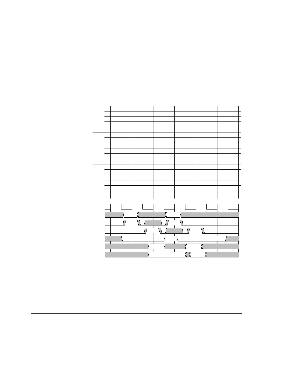
Coprocessor Interface
7-24
Copyright © 2003 ARM Limited. All rights reserved.
ARM DDI 0244C
In Figure 7-4 ASTOPCPD is used to indicate that instruction 1 stalled in the
ARM1026EJ-S Decode stage for one cycle. The following values of CPINSTR,
CPINSTRV, and CPVALIDD are invalid in all but the last cycle that was interlocked.
ASTOPCPD is LOW as instruction 2 leaves the Decode stage indicating that it was not
held up. The numbers in waveforms show which instruction owns the signal at that
time.
Figure 7-4 ASTOPCPD example
CPLSLEN, CPLSSWP, and CPLSDBL for a given instruction are driven from a CP
in the cycle before ASTOPCPD is driven from the ARM1026EJ-S processor, so the
ARM1026EJ-S processor must register the value of CPLSLEN and CPLSSWP and
CPLSDBL if it is about to drive an ASTOPCPD.
I1
I1
I2
I1
I1
I2
I1
I1
I2
I
D
E
M
W
F
I
M
W
F
I
M
W
I1
I2
I2
I1
I1
I1
I1
I2
I2
I2
I2
I2
ARM
CP1
CP2
D
E
D
E
T1
T2
T3
T4
T5
T6
T7
1
2
1
2
1
CPINSTR
CPINSTRV
CPCLK
CPVALIDD
ASTOPCPD
I1
CPLSLEN/SWP/DBL
CPLSLEN/SWP/DBL (internal)
1
2
2
1
1
1
2
2
2

Coprocessor Interface
ARM DDI 0244C
Copyright © 2003 ARM Limited. All rights reserved.
7-25
7.8.2
ASTOPCPE
ASTOPCPE indicates that the instruction in the ARM1026EJ-S Execute stage did not
progress into the ARM1026EJ-S Memory stage in the previous cycle. It is driven out of
a register following the ARM1026EJ-S Execute stage. If ASTOPCPE is asserted, CPs
must hold their Execute, Decode, Issue, and Fetch stages. The logic in these stages must
keep reevaluating as CPINSTR, CPINSTRV, and CPVALIDD might change. Only
the cycle where ASTOPCPE is deasserted is a valid cycle. AFLUSHCP overrides
ASTOPCPE.
The ARM1026EJ-S processor drives ASTOPCPE in ARM1026EJ-S Execute + 1
stage and the CP Execute stage.
7.8.3
ASTOPCPE example
Figure 7-5 on page 7-26 shows the ARM1026EJ-S processor holding instruction 1 in its
Execute stage for one cycle. The numbers in the waveforms show which instruction
owns the signal at that time.
Table 7-10 ASTOPCPE interactions with other signals
Signal
Interactions with ASTOPCPD
ASTOPCPD
None.
LSHOLDCPE
ASTOPCPE is asserted with LSHOLDCPE when the pipelines are in lockstep. Pipelines are in
lockstep unless the CP has already retired from the ARM1026EJ-S pipeline and is now transferring
data from the LSU for a load/store multiple.
CPBUSYE
The ARM1026EJ-S processor ignores CPBUSYE if ASTOPCPE is already asserted. ASTOPCPE is
not asserted if CPBUSYE was asserted at the end of the previous cycle, but ASTOPCPE can be
asserted when CPBUSYE deasserts. In this case, asserting ASTOPCPE continues to hold the same
instruction in ARM1026EJ-S Execute that was held by CPBUSYE.
LSHOLDCPM
ASTOPCPE is asserted with LSHOLDCPM when the pipelines are in lockstep. Pipelines are in
lockstep unless the CP has already retired from the ARM1026EJ-S pipeline and is now transferring
data from the LSU for a load/store multiple.
ACANCELCP
ACANCELCP held by ASTOPCPE.
AFLUSHCP
AFLUSHCP overrides ASTOPCPE. The pipeline is flushed from Execute back.
CPBOUNCEE
CPBOUNCEE is not used until ASTOPCPE (and other relevant holds) are deasserted.
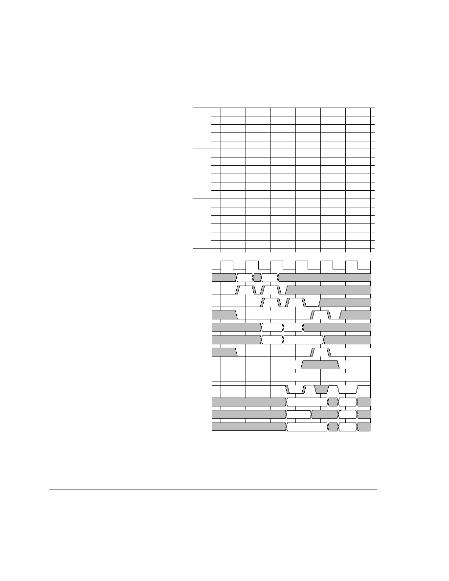
Coprocessor Interface
7-26
Copyright © 2003 ARM Limited. All rights reserved.
ARM DDI 0244C
Figure 7-5 ASTOPCPE example
* ASTOPCPD is caused by ASTOPCPE and CPBUSYE is ignored under
ASTOPCPE. Under an ASTOPCPE, STC is registered in the ARM1026EJ-S
processor.
1
2
1
2
1
I1
I1
I2
I1
I1
I2
I1
I1
I
D
E
M
W
F
I
M
W
F
I
M
W
I1
I2
I2
I1
I1
I1
I1
I2
I2
I2
I2
I2
ARM
CP1
CP2
D
E
D
E
T1
T2
T3
T4
T5
T6
T7
2
1
2
1
CPINSTR
CPINSTRV
CPCLK
CPVALIDD
ASTOPCPD
I1
ASTOPCPE
CPLSLEN/SWP/DBL
CPBUSYE
1
2
1
2
2*
1
CPLSLEN/SWP/DBL (internal)
2
1
2
2
CPBUSYE (internal)
CPBOUNCEE
CPBOUNCEE (internal)
I2
2
1
STC
STC (internal)
1
2
1
2
1
1
2
1
1

Coprocessor Interface
ARM DDI 0244C
Copyright © 2003 ARM Limited. All rights reserved.
7-27
7.8.4
LSHOLDCPE
LSHOLDCPE indicates that the load/store CP instruction in the ARM1026EJ-S LSU
Execute stage, did not progress into the ARM1026EJ-S LSU Memory stage in the
previous cycle. It is driven out of a register following the ARM1026EJ-S LSU Execute
stage. If LSHOLDCPE is asserted, CPs must hold their Execute, Decode, Issue, and
Fetch stages. If LSHOLDCPE is asserted, and a store is in the CP Execute stage, the
STCMRCDATA bus value is retained by the ARM1026EJ-S processor until
LSHOLDCPE deasserts.
The ARM1026EJ-S processor drives LSHOLDCPE in the ARM1026EJ-S
Execute + 1 stage and the CP Execute stage.
7.8.5
Example of LSHOLDCPE
Figure 7-6 on page 7-28 shows the ARM1026EJ-S LSU holding instruction 1 in its
Execute stage for one cycle. The numbers in the waveforms show which instruction
owns the signal at that time. ASTOPCPD is caused by ASTOPCPE. CPBUSYE is
ignored under ASTOPCPE. Under an LSHOLDCPE, STC is registered in the
ARM1026EJ-S processor.
Table 7-11 LSHOLDCPE interactions with other signals
Signal
Interactions with LSHOLDCPE
ASTOPCPD
None.
LSHOLDCPE
None.
ASTOPCPE
LSHOLDCPE is asserted with ASTOPCPE when pipelines are in lockstep. Pipelines are in lockstep
unless the CP instruction has already retired from the ALU pipeline and is now transferring data to or
from the LSU.
CPBUSYE
CPBUSYE indicates an Execute stage hold when the ALU and LSU pipelines are in lockstep.
LSHOLDCPE indicates an LSU execute stage hold when the ALU and LSU pipelines are not in
lockstep.
LSHOLDCPM
If LSHOLDCPM is asserted, LSHOLDCPE is asserted as well.
ACANCELCP
None.
AFLUSHCP
Flush invalidates LSHOLDCPE.
CPBOUNCEE
None.

Coprocessor Interface
7-28
Copyright © 2003 ARM Limited. All rights reserved.
ARM DDI 0244C
Figure 7-6 LSHOLDCPE example
2
I1
I1
I2
I1
I1
I2
I1
I1
I2
I
D
E
M
W
F
I
M
W
F
I
M
W
I1
I2
I2
I1
I1
I1
I1
I2
I2
I2
I2
I2
ARM
CP1
CP2
D
E
D
E
T1
T2
T3
T4
T5
T6
T7
1
2
1
2
1
CPINSTR
CPINSTRV
CPCLK
CPVALIDD
ASTOPCPD
I1
CPLSLEN/SWP/DBL
CPLSLEN/SWP/DBL (internal)
1
2
2
2
2
1
2
2
ASTOPCPE
1
1
LSHOLDCPE
CPBUSYE
CPBUSYE (internal)
CPBOUNCEE
CPBOUNCEE (internal)
1
2
1
1
1
2
1
1
1
2
STCMRCDATA
1
2
STCMRCDATA (internal)
1
1
2

Coprocessor Interface
ARM DDI 0244C
Copyright © 2003 ARM Limited. All rights reserved.
7-29
7.8.6
LSHOLDCPM
LSHOLDCPM indicates that the load CP instruction in the ARM1026EJ-S LSU
Memory stage did not progress into the ARM1026EJ-S LSU Write stage in the previous
cycle or that a load cache miss occurred. It is driven out of a register following the
ARM1026EJ-S LSU Memory stage. If LSHOLDCPM is asserted, CPs must hold their
Memory, Execute, Decode, Issue and Fetch stages. If LSHOLDCPM is asserted, and
a load is in the CP Memory stage, the LDCMCRDATA bus value is ignored by the CP
until LSHOLDCPM deasserts.
The ARM1026EJ-S processor drives LSHOLDCPM in the ARM1026EJ-S
Memory + 1 stage and the CP Memory stage.
Table 7-12 LSHOLDCPM interactions with other signals
Signal
Interactions with other signals
ASTOPCPD
None
LSHOLDCPE
None
ASTOPCPE
None
CPBUSYE
None
LSHOLDCPM
If LSHOLDCPM is asserted, LSHOLDCPE is also asserted
ACANCELCP
None
AFLUSHCP
None
CPBOUNCEE
None
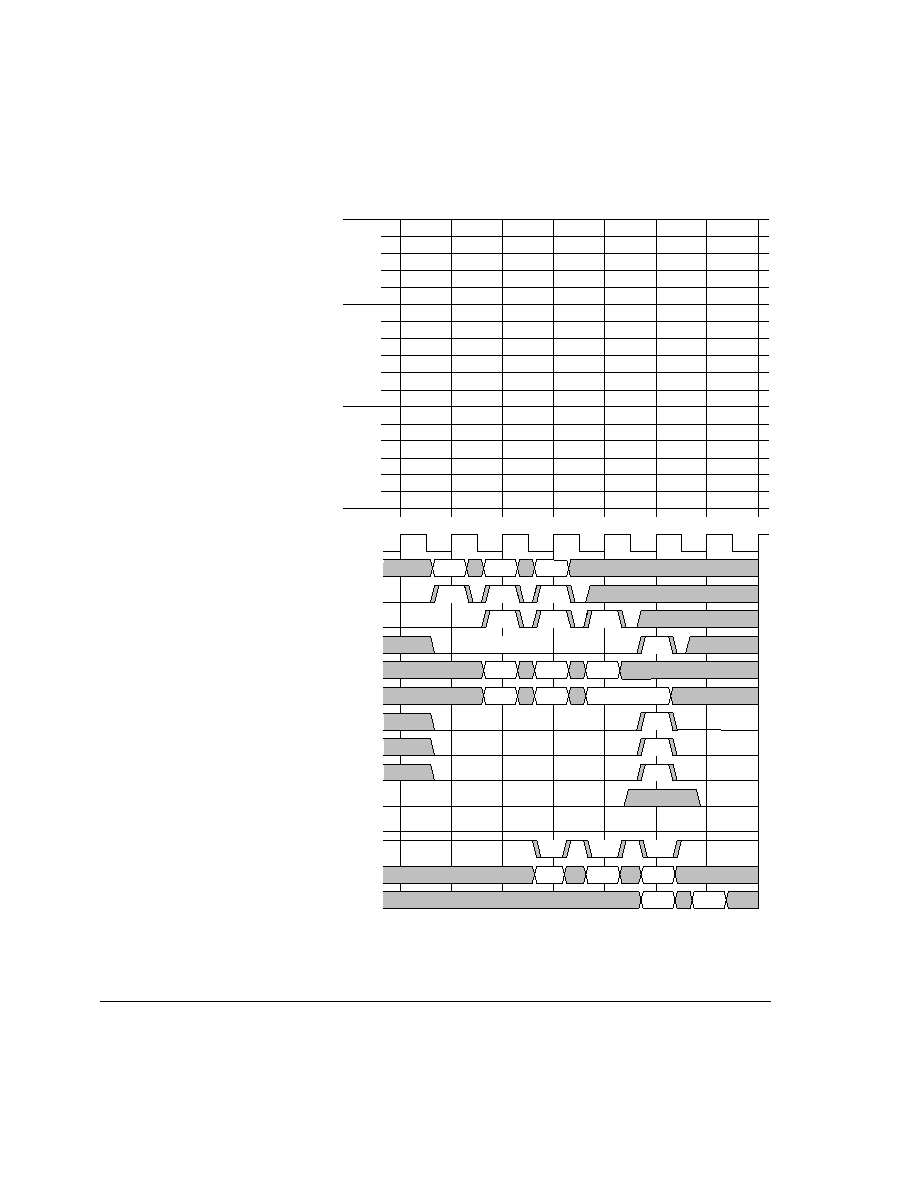
Coprocessor Interface
7-30
Copyright © 2003 ARM Limited. All rights reserved.
ARM DDI 0244C
Figure 7-7 LSHOLDCPM example
1
3
3
3
3
3
1
2
I1
I1
I2
I1
I1
I2
I1
I1
I2
I
D
E
M
W
F
I
M
W
F
I
M
W
I1
I2
I2
I1
I1
I1
I1
I2
I2
I2
I2
I2
ARM
CP1
CP2
D
E
D
E
T1
T2
T3
T4
T5
T6
T7
2
1
2
1
CPINSTR
CPINSTRV
CPCLK
CPVALIDD
ASTOPCPD
I1
ASTOPCPE
CPLSLEN/SWP
LSHOLDCPE
1
2
3
1
2
3
1
CPLSLEN/SWP (internal)
T8
3
2
2
1
LSHOLDCPE
CPBUSYE
CPBUSYE (internal)
CPBOUNCEE
CPBOUNCEE (internal)
LDCMCRDATA
2
1
2
3
x
1
I3
I3
I3
I3
I3
I2
I1
I2

Coprocessor Interface
ARM DDI 0244C
Copyright © 2003 ARM Limited. All rights reserved.
7-31
7.8.7
CPBUSYE
From the ARM1026EJ-S processor viewpoint, CPBUSYE indicates that the CP that
owns the instruction in the ARM1026EJ-S Execute stage wants to hold the instruction
in that stage. It is asserted in the ARM1026EJ-S Execute stage and must come directly
out of a register. It also holds the instructions in other CP Issue stages. Table 7-13 shows
the interaction of CPBUSYE with other signals.
The ARM1026EJ-S processor drives CPBUSYE in the ARM1026EJ-S Execute stage
and the CP Decode stage.
Table 7-13 CPBUSYE interactions with other signals
Signal
interactions with CPBUSYE
ASTOPCPD
The ARM1026EJ-S processor ignores CPBUSYE if ASTOPCPD is already asserted. ASTOPCPD
is not asserted if a valid CPBUSYE (CPBUSY HIGH, ASTOPCPD LOW) was received in the
previous cycle.
ASTOPCPE
The ARM1026EJ-S processor ignores CPBUSYE if ASTOPCPE is already active. ASTOPCPE is
not asserted if a valid CPBUSYE was asserted at the end of the previous cycle. ASTOPCPE is not
asserted if CPBUSYE is already asserted. ASTOPCPE can be asserted in the cycle that CPBUSYE
deasserts.
LSHOLDCPE
None.
LSHOLDCPM
None.
ACANCELCP
None.
AFLUSHCP
AFLUSHCP has priority over CPBUSYE.
CPBOUNCEE
CPBOUNCEE is not used until CPBUSYE (and other holds) are deasserted.
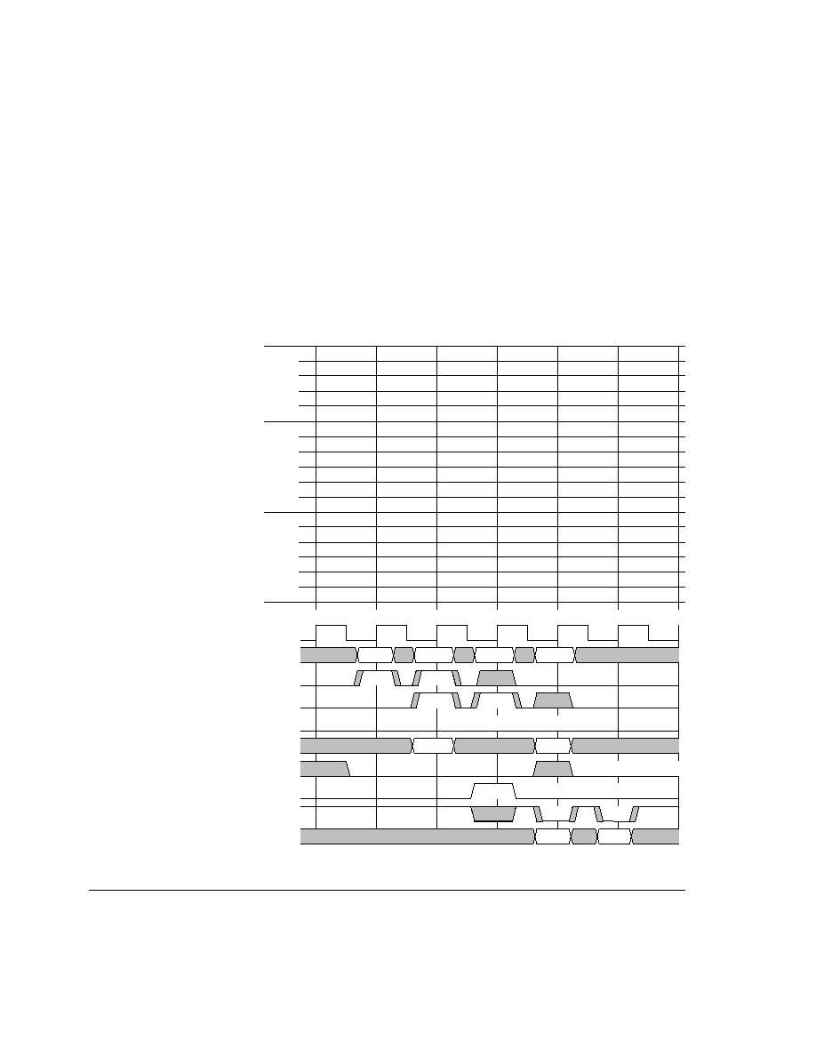
Coprocessor Interface
7-32
Copyright © 2003 ARM Limited. All rights reserved.
ARM DDI 0244C
7.8.8
CPBUSYE example
In Figure 7-8, instruction 1 is held in the ARM1026EJ-S Execute stage by CPBUSYE.
Numbers in waveforms show which instruction owns the signal at that time. In some
CPs, instruction 1 might advance into Decode under the CPBUSYE. In this case,
instruction 1 spends two cycles in Decode rather than in Issue. This depends on the CP
implementation. For the interface this makes no difference because the interface signals
still have to be driven depending upon the position of the instruction in the
ARM1026EJ-S pipeline.
Figure 7-8 CPBUSYE example
I1
I1
I2
I1
I1
I2
I1
I1
I2
I
D
E
M
W
F
I
M
W
F
I
M
W
I1
I2
I2
I1
I1
I1
I1
I2
I2
I2
I2
I2
ARM
CP1
CP2
D
E
D
E
T1
T2
T3
T4
T5
T6
T7
1
2
1
2
1
CPINSTR
CPINSTRV
CPCLK
CPVALIDD
ASTOPCPD
I1
CPLSLEN/SWP
1
2
2
2
1
CPBUSYE
CPBOUNCEE
2
2
STCMRCDATA
I3
I3
x
3
1
ASTOPCPE
1
2
1
1
2
1
2
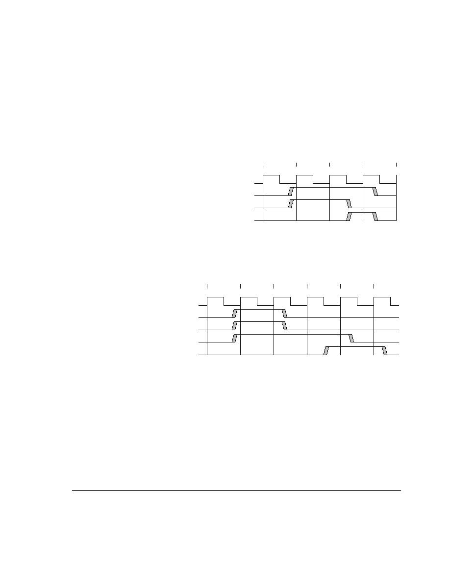
Coprocessor Interface
ARM DDI 0244C
Copyright © 2003 ARM Limited. All rights reserved.
7-33
7.8.9
CPBUSYE and ASTOPCPD interaction
There is a complex interaction between ASTOPCPD and CPBUSYE. If ASTOPCPD
and CPBUSYE are asserted in the same cycle, the ARM1026EJ-S processor ignores
CPBUSYE until ASTOPCPD deasserts. Figure 7-9 shows one possible sequence of
events.
Figure 7-9 CPBUSYE ignored due to ASTOPCPD assertion
If CPBUSYE is asserted in the cycle before the ARM1026EJ-S processor would have
asserted ASTOPCPD, then ASTOPCPD is suppressed until the cycle after CPBUSYE
deasserts. Figure 7-10 shows this sequence of events.
Figure 7-10 CPBUSYE asserted before ASTOPCPD
The internal hold signal HOLDD is usually registered to make ASTOPCPD in the next
cycle, but this is held until CPBUSYE goes LOW.
T2
T1
T3
T4
T5
CPCLK
CPBUSYE
ASTOPCPD
CPBUSYE (internal)
T2
T1
T3
T4
T5
CPCLK
CPBUSYE
CPBUSYE (internal)
HOLDD (internal)
ASTOPCPD
T6

Coprocessor Interface
7-34
Copyright © 2003 ARM Limited. All rights reserved.
ARM DDI 0244C
7.8.10
ASTOPCPD with CPBUSYE
In Figure 7-11, instruction 1 is held up by CPBUSYE and instruction 2 is held up by
ASTOPCPD. An instruction in ARM1026EJ-S Decode is always held up behind an
instruction held by ARM1026EJ-S CPBUSYE in Execute, unless it is flushed.
Figure 7-11 ASTOPCPD with CPBUSYE
I1
I1
I2
I1
I1
I2
I1
I2
I1
I
D
E
M
W
F
I
M
W
F
I
M
W
I1
I2
I1
I2
I1
I2
I1
I1
I1
I1
I2
I2
I2
I2
I2
I2
ARM
CP1
CP2
D
E
D
E
T1
T2
T3
T4
T5
T6
T7
T8
1
x
2
2
1
x
1
1
2
1
2
2
2
x
1
2
2
CPINSTR
CPINSTRV
CPCLK
CPVALIDD
CPBUSYE
CPLSLEN/SWP/DBL
ASTOPCPD
CPBOUNCEE
STCMRCDATA
ASTOPCPD (internal)
2
1
3
2
1
x
1
I1

Coprocessor Interface
ARM DDI 0244C
Copyright © 2003 ARM Limited. All rights reserved.
7-35
7.8.11
CPBUSYE and ASTOPCPE interaction
There is a complex interaction between ASTOPCPE and CPBUSYE. CPBUSYE is
asserted in the Execute stage of an instruction, ASTOPCPE is asserted from a register
at the end of the Execute stage (E + 1). If ASTOPCPE is asserted in the same cycle that
CPBUSYE is asserted then CPBUSYE is ignored until ASTOPCPE deasserts. If
CPBUSYE is asserted in the previous cycle then ASTOPCPE cannot be asserted until
the cycle after that in which CPBUSYE deasserts.
Where ASTOPCPE is asserted at the same time as CPBUSYE, the ARM1026EJ-S
processor ignores CPBUSYE until ASTOPCPE deasserts. In Figure 7-12, CPBUSYE
is ignored until ASTOPCPE deasserts.
Figure 7-12 CPBUSYE ignored due to ASTOPCPE assertion
In Figure 7-13, CPBUSYE is asserted before ASTOPCPE. The ARM1026EJ-S
processor does not assert ASTOPCPE until the cycle after CPBUSYE deasserts.
ASTOPCPE is holding up the same instruction, in Execute, that CPBUSYE held up.
Figure 7-13 CPBUSYE asserted before ASTOPCPE
T2
T1
T3
T4
T5
CPCLK
CPBUSYE
ASTOPCPE
CPBUSYE (internal)
CPCLK
CPBUSYE
HOLDE (internal)
ASTOPCPE
CPBUSYE (internal)
T2
T1
T3
T4
T5
T6

Coprocessor Interface
7-36
Copyright © 2003 ARM Limited. All rights reserved.
ARM DDI 0244C
7.8.12
ASTOPCPE with CPBUSYE
In Figure 7-14, instruction 2 is held up by ASTOPCPE and CPBUSYE.
Figure 7-14 I2 held up by ASTOPCPE and CPBUSYE
*Although instruction 3 is responsible for ASTOPCPD at T7, instruction 2 causes
ASTOPCPE to be asserted, and this has to be folded back into ASTOPCPD.
I1
I1
I2
I1
I1
I2
I1
I3
I
D
E
M
W
F
I
M
W
F
I
M
W
I2
I3
I2
I3
I2
I3
I1
I1
I1
I1
I2
I3
I2
I3
I2
I3
I2
I3
I2
I3
I2
I3
ARM
CP1
CP2
D
E
D
E
T1
T2
T3
T4
T5
T6
T7
T8
1
3
2
3
2
1
3
3
2
1
3
1
2
2
2
3
1
2
2
3
3
3*
3
3
1
1
1
2
2
3
x
1
2
1
3
2
3
2
x
1
CPINSTR
CPINSTRV
CPCLK
CPVALIDD
CPBUSYE
CPLSLEN/SWP
ASTOPCPE
CPBOUNCEE
STCMRCDATA
ASTOPCPD
CPBUSYE (internal)
HOLD E (internal)
2
1
2
2
3
I2
I1
I3
I2
I1
I3
I2
2

Coprocessor Interface
ARM DDI 0244C
Copyright © 2003 ARM Limited. All rights reserved.
7-37
In Figure 7-15, instruction 1 is held up by ASTOPCPE and instruction 2 is held up by
CPBUSYE.
Figure 7-15 I1 held up by ASTOPCPE and I2 held up by CPBUSYE
*Although instruction 2 is responsible for driving ASTOPCPD at T5, instruction 1
causes ASTOPCPE to be asserted, and this has to be folded back into ASTOPCPD.
I1
I1
I2
I1
I1
I2
I1
I2
I1
I3
I3
I
D
E
M
W
F
I
M
W
F
I
M
W
I2
I1
I3
I2
I3
I2
I3
I2
I3
I1
I1
I1
I1
I2
I3
I2
I3
I2
I3
I2
I3
I2
I3
I2
I3
ARM
CP1
CP2
D
E
D
E
T1
T2
T3
T4
T5
T6
T7
T8
1
3
2
3
2
1
3
3
2
1
3
1
2
2
2
3
1
2
2
3
2*
3
3
2
1
1
1
2
2
3
3
x
1
2
1
3
2
3
x
x
1
2
CPINSTR
CPINSTRV
CPCLK
CPVALIDD
CPBUSYE
CPLSLEN/
SWP/DBL
ASTOPCPE
CPBOUNCEE
STCMRCDATA
ASTOPCPD
CPBUSYE (internal)
HOLD E (internal)
2
1
1
2
3

Coprocessor Interface
7-38
Copyright © 2003 ARM Limited. All rights reserved.
ARM DDI 0244C
In Figure 7-16, instruction 1 is held up by CPBUSYE and instruction 2 is held up by
ASTOPCPD.
Figure 7-16 I1 held up by CPBUSYE and I2 held up by ASTOPCPD
*Although instruction 3 is responsible for driving ASTOPCPE at T7, instruction 2
causes ASTOPCPE to be asserted, and this has to be folded back into ASTOPCPD.
I1
I1
I2
I1
I1
I2
I1
I2
I1
I3
I3
I
D
E
M
W
F
I
M
W
F
I
M
W
I2
I1
I3
I1
I2
I3
I2
I3
I2
I3
I1
I1
I1
I1
I1
I2
I3
I2
I3
I2
I3
I2
I3
I2
I3
I2
I3
I2
ARM
CP1
CP2
D
E
D
E
T1
T2
T3
T4
T5
T6
T7
T8
CPCLK
CPINSTR
1
x
3
2
CPINSTRV
x
2
1
3
CPVALIDD
3
2
1
CPBUSYE
1
2
1
3
HOLD E (internal)
2
1
1
2
3
CPBUSYE (internal)
1
2
1
3
ASTOPCPD
3*
3
2
2
1
ASTOPCPE
1
1
2
2
3
CPLSLEN/
SWP/DBL
3
2
1
3
CPBOUNCEE
x
1
2
3
STCMRCDATA
3
2
1
x

Coprocessor Interface
ARM DDI 0244C
Copyright © 2003 ARM Limited. All rights reserved.
7-39
7.8.13
CPLSBUSY
This is driven out of a register on the CP Issue/Decode boundary (valid early in the
ARM1026EJ-S Execute stage). It signals to other CPs that the sender is involved in a
load or store multiple data transfer and is keeping control of the STCMRCDATA bus.
Other CPs must progress to Decode (where they are stalled by ASTOPCPE) but must
not attempt to drive the bus until a cycle after CPLSBUSY deasserts.
CPLSBUSY stalls all other CPs when a long LDC is in progress. CPLSBUSY does not
have to go to the ARM1026EJ-S processor because it can only do one load/store
operation at a time because they are held up in any case. CPLSBUSY comes out of flop
and goes to other CPs.
The CP drives CPLSBUSY in the CP Decode stage and the ARM1026EJ-S Execute
stage.
Table 7-14 CPLSBUSY interactions with other signals
Signal
Interactions with CPLSBUSY
ASTOPCPD
None
ASTOPCPE
None
LSHOLDCPE
None
LSHOLDCPM
None
ACANCELCP
None
AFLUSHCP
None
CPBOUNCEE
None

Coprocessor Interface
7-40
Copyright © 2003 ARM Limited. All rights reserved.
ARM DDI 0244C
7.9
Instruction cancelation
Instruction cancelation signals are described in the following sections:
∑
ACANCELCP
∑
ACANCELCP example on page 7-41
∑
ACANCELCP with ASTOPCPE example on page 7-42
∑
ACANCELCP with CPBUSYE example on page 7-43
∑
AFLUSHCP on page 7-44
∑
AFLUSHCP example on page 7-44.
7.9.1
ACANCELCP
ACANCELCP indicates that the instruction that has just entered the ARM1026EJ-S
Memory stage must be canceled. ACANCELCP differs from AFLUSHCP. It cancels
a single instruction rather than canceling all upstream instructions in the pipeline. It is
driven from register following the ARM1026EJ-S Execute stage. Table 7-15 shows
ACANCELCP the interactions with other signals.
The ARM1026EJ-S processor drives ACANCELCP in the ARM1026EJ-S Memory
stage and the CP Execute stage.
Table 7-15 ACANCELCP interactions with other signals
Signal
Interactions with CPBUSYE
ASTOPCPD
None
ASTOPCPE
CP ignores ACANCELCP if ASTOPCPE asserted
LSHOLDCPE
None
CPBUSYE
ACANCELCP is held is response to an active CPBUSYE
LSHOLDCPM
None
ACANCELCP
None
AFLUSHCP
AFLUSHCP has priority
CPBOUNCEE
No effect for canceled instructions
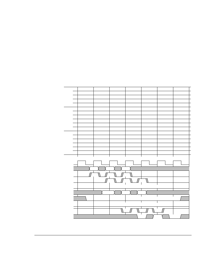
Coprocessor Interface
ARM DDI 0244C
Copyright © 2003 ARM Limited. All rights reserved.
7-41
7.9.2
ACANCELCP example
ACANCELCP cancels one instruction (turns it into a NOP) but does not affect the ones
around it. In this case, three instructions are issued in a row. Instruction 2 is canceled.
Instructions 1 and 3 complete. The numbers in waveforms show which instruction owns
the signal at that time. The ARM1026EJ-S processor ignores an indication from CP2
that I2 must bounce as the instruction is canceled. Figure 7-17 shows an example with
ACANCELCP.
Figure 7-17 ACANCELCP example
I1
I1
I2
I1
I1
I2
I1
I2
I1
I3
I3
I
D
E
M
W
F
I
M
W
F
I
M
W
I1
I3
I3
I3
I1
I1
I1
I1
I2
I3
I2
I3
I2
I3
I2
I3
I3
ARM
CP1
CP2
D
E
D
E
T1
T2
T3
T4
T5
T6
T7
1
3
2
3
2
1
2
1
3
1
3
2
3
2
2
1
1
3
2
3
CPINSTR
CPINSTRV
CPCLK
CPVALIDD
ASTOPCPD
ASTOPCPE
CPBOUNCEE
ACANCELCP
3
3
1
2
CPLSLEN/
SWP/DBL
CPBUSYE
1
3
2
1
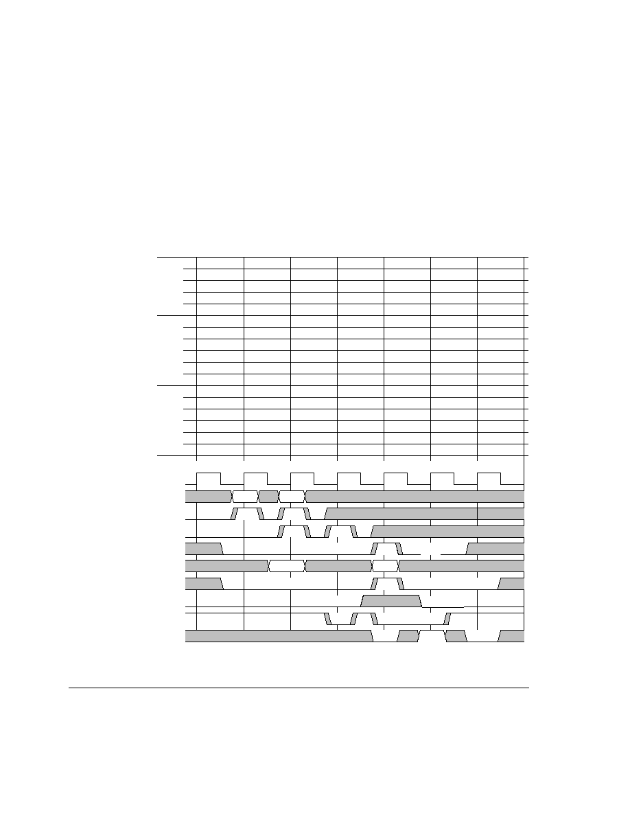
Coprocessor Interface
7-42
Copyright © 2003 ARM Limited. All rights reserved.
ARM DDI 0244C
The ARM1026EJ-S processor ignores an indication from CP2 that instruction 2 must
bounce because the instruction is canceled.
7.9.3
ACANCELCP with ASTOPCPE example
Instruction 1 is held up by the ARM1026EJ-S processor with ASTOPCPE.
ACANCELCP is valid in the last cycle that ASTOPCPE is asserted. Figure 7-18
shows an example of ACANCELCP with ASTOPCPE.
Figure 7-18 ACANCELCP with ASTOPCPE example
2
I1
I1
I2
I1
I1
I2
I1
I1
I2
I
D
E
M
W
F
I
M
W
F
I
M
W
I1
I2
I2
I2
I1
I1
I1
I1
I2
I2
I2
I2
I2
I2
ARM
CP1
CP2
D
E
D
E
T1
T2
T3
T4
T5
T6
T7
1
2
2
1
2
1
1
2
2
1
1
1
2
CPINSTR
CPINSTRV
CPCLK
CPVALIDD
ASTOPCPD
ASTOPCPE
CPBOUNCEE
ACANCELCP
3
2
1
CPLSLEN/SWP/DBL
CPBUSYE
1
2
1
x
1
2
I1
I1
2
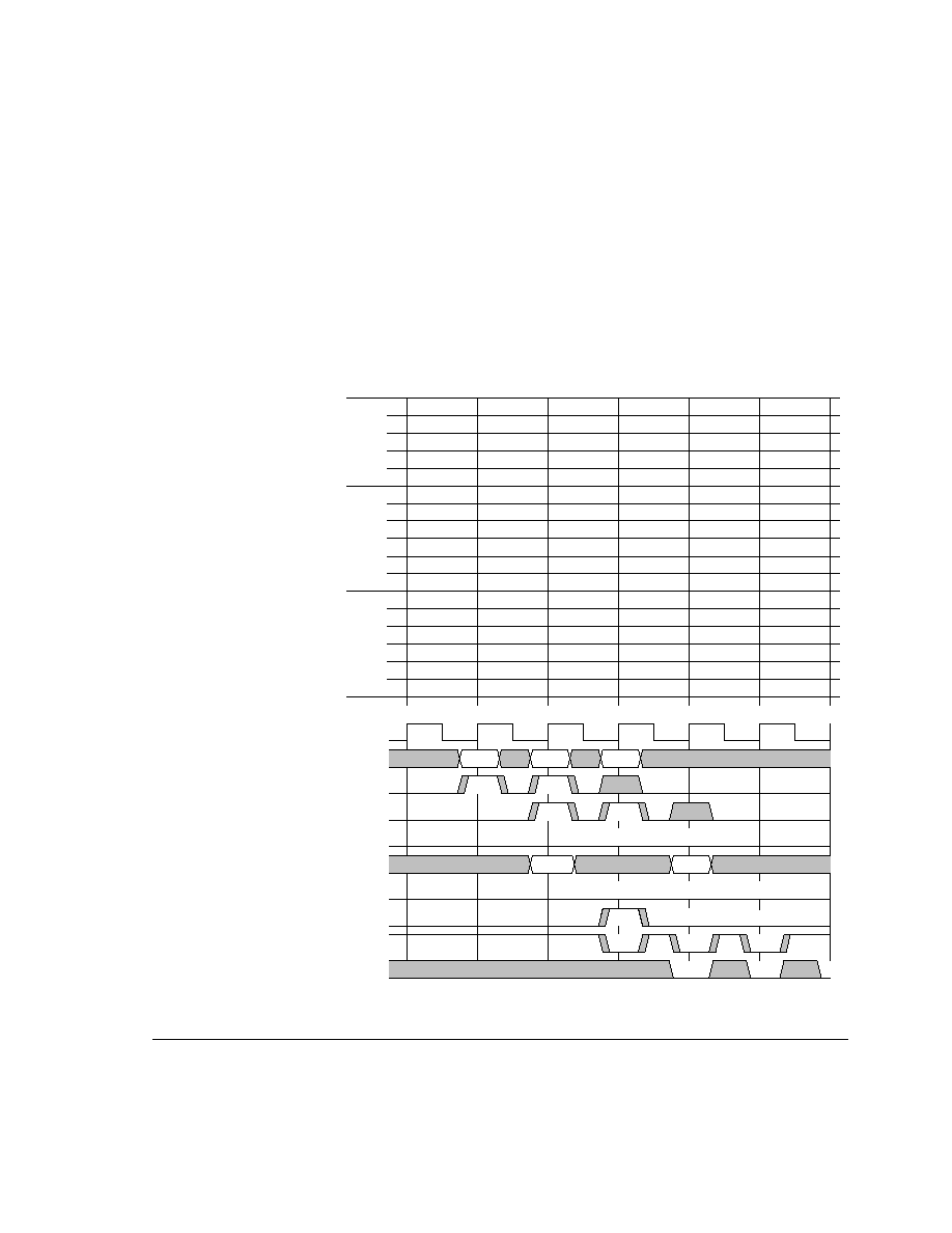
Coprocessor Interface
ARM DDI 0244C
Copyright © 2003 ARM Limited. All rights reserved.
7-43
7.9.4
ACANCELCP with CPBUSYE example
Instruction 1 is held up by CP1 as indicated by CPBUSYE. ACANCELCP is valid in
the last cycle that CPBUSYE is asserted.
ASTOPCPE might be asserted with CPBUSYE. It can then be deasserted while
CPBUSYE is still active or might have stayed asserted when CPBUSYE is deasserted.
When both CPBUSYE and ASTOPCPE are deasserted the pipeline must progress.
Figure 7-19 shows an example of ACANCELCP with CPBUSYE.
Figure 7-19 ACANCELCP with CPBUSYE example
2
I1
I1
I2
I1
I1
I2
I1
I1
I2
I
D
E
M
W
F
I
M
W
F
I
M
W
I1
I2
I2
I1
I1
I1
I1
I2
I2
I2
I2
I2
ARM
CP1
CP2
D
E
D
E
T1
T2
T3
T4
T5
T6
T7
1
2
2
1
2
1
1
2
1
x
1
1
2
CPINSTR
CPINSTRV
CPCLK
CPVALIDD
ASTOPCPD
ASTOPCPE
CPBOUNCEE
ACANCELCP
2
1
CPLSLEN/SWP/DBL
CPBUSYE
1
2
2
x
I1
x
1
1

Coprocessor Interface
7-44
Copyright © 2003 ARM Limited. All rights reserved.
ARM DDI 0244C
7.9.5
AFLUSHCP
AFLUSHCP indicates that the instruction that has just entered the ARM1026EJ-S
Memory stage and all upstream instructions currently in the pipeline must be canceled.
AFLUSHCP differs from ACANCELCP because it cancels all upstream instructions
in the pipeline rather than just a single instruction. It is driven from register following
the ARM1026EJ-S Execute stage. This means that there is no time to factor Data Aborts
into the AFLUSHCP signal. As a result, aborted CP loads complete when a Data Abort
occurs, and then be reexecuted on return from the Data Abort handler routine. It must
be possible to execute any CP load more than once (before the next instruction is
executed) with no noticeable effects on the CP.
The ARM1026EJ-S processor drives AFLUSHCP in the ARM1026EJ-S Memory
stage and the CP Execute stage.
AFLUSHCP supersedes the ASTOP and VALID signals from the ARM1026EJ-S
processor. It is used to signal that an interrupt has flushed the pipeline. As a result
CPBUSYE must be deasserted in the following cycle to enable the interrupt to be
serviced.
7.9.6
AFLUSHCP example
AFLUSHCP has to override ASTOPCPE and ASTOPCPD. Here AFLUSHCP is
asserted for instruction 2. This might be caused by instruction 2 being bounced or a
reason unrelated to the CPs, an interrupt, for example. AFLUSHCP has to kill the
effects of instruction 2 and all following instructions currently in the pipe.
Table 7-16 AFLUSHCP interactions with other signals
Signal
Interactions with CPBUSYE
ASTOPCPD
Flush overrides
ASTOPCPE
Flush overrides
LSHOLDCPE
Flush overrides
CPBUSYE
Flush overrides (deasserted in the following cycle)
LSHOLDCPM
Flush overrides
ACANCELCP
None
CPBOUNCEE
Ignored because instruction canceled by flush
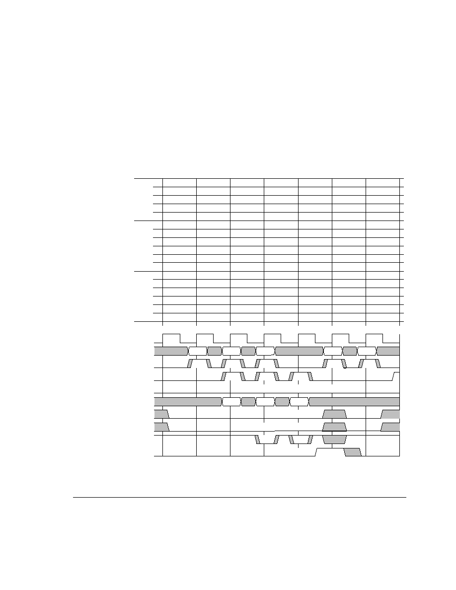
Coprocessor Interface
ARM DDI 0244C
Copyright © 2003 ARM Limited. All rights reserved.
7-45
Interrupts can cause flushes at any time. So, even a valid instruction that has been
busy-waited for many cycles can be flushed. When the instruction has reached the
Memory stage of the ARM1026EJ-S processor without AFLUSHCP or
ACANCELCP being asserted it completes (with the exception of instructions that Data
Abort). Figure 7-20 shows an example of this with five instructions. CP load or store
instructions that cause a Data Abort are completed by the CP and rerun by the Data
Abort handler. So they must be designed to be rerun with no ill effects.
Figure 7-20 AFLUSHCP example
2
I1
I1
I2
I1
I1
I2
I1
I2
I3
I
D
E
M
W
F
I
M
W
F
I
M
W
I1
I1
I1
I1
I2
I3
I3
I3
ARM
CP1
CP2
D
E
D
E
T1
T2
T3
T4
T5
T6
T7
1
2
2
1
2
1
1
2
1
1
2
CPINSTR
CPINSTRV
CPCLK
CPVALIDD
ASTOPCPD
ASTOPCPE
CPBOUNCEE
AFLUSHCP
2
1
CPLSLEN/SWP/DBL
CPBUSYE
1
2
2
1
I1
3
2
T8
4
5
3
4
5
3
3
I3
I1
[I4]
I5
I2
I2
I4
I2
I5
3

Coprocessor Interface
7-46
Copyright © 2003 ARM Limited. All rights reserved.
ARM DDI 0244C
The ARM1026EJ-S processor ignores an indication from CP2 that I2 might bounce as
the instruction is canceled. Instruction 4 might be in the Issue stage. This must be
flushed by AFLUSHCP but is also not confirmed by CPVALIDD. Instruction 5 is
issued after the flush and is a valid instruction.
AFLUSHCP can be asserted even if hold signals such as ACANCELCP and/or
CPBUSYE are asserted. In these cases, AFLUSHCP has the highest priority because
the pipe is currently full of instructions that do not execute. This might be because of a
mispredicted branch or an exception.

Coprocessor Interface
ARM DDI 0244C
Copyright © 2003 ARM Limited. All rights reserved.
7-47
7.10
Bounced instructions
The following sections describe what happens when CPs cannot execute an instruction,
and the undefined instruction trap must be taken:
∑
CPBOUNCEE
∑
CPBOUNCEE example on page 7-49
∑
CPBOUNCEE with ASTOPCPE on page 7-51
∑
CPBOUNCEE with CPBUSYE on page 7-52.
7.10.1
CPBOUNCEE
CPBOUNCEE is used by CPs to acknowledge ownership of CP instructions. Only a
CP with an ID that matches the CPID field in the instruction can accept an instruction.
If no CP accepts an instruction, the instruction is bounced to an Undefined Instruction
handler, and the undefined instruction trap is taken. A CP does not have to accept all
instructions with an CPID that matches its ID. This enables using a mixture of hardware
and software to implement a CP.
The CP drives CPBOUNCEE out of a register at the start of the ARM1026EJ-S
Execute stage. When an instruction is bounced, the CP should continue to operate as if
it were a NOP. If the bounced instruction passes its condition code check then the
ARM1026EJ-S processor indicates that the CP should flush its pipeline using
AFLUSHCP.
The CP that owns an instruction on the CPINSTR bus drives LOW the CPBOUNCEE
signal to the ARM1026EJ-S processor in the CP Decode stage. If the instruction is not
owned by a CP, that CP leaves CPBOUNCEE HIGH. The ARM1026EJ-S processor
ANDs all individual CPBOUNCEE signals internally. If CPBOUNCEE is HIGH
across ARM1026EJ-S Execute/Memory boundary, the instruction is deemed to have
not been accepted by any CP, and the Undefined instruction trap is taken. A CP can
bounce an instruction if the CP is unable to process that instruction or is unable to
process a prior instruction and requires software support.
The ARM1026EJ-S processor ignores CPBOUNCEE if CPBUSYE is asserted and
registers the value of CPBOUNCEE at the end of the cycle that CPBUSYE deasserts.
An active ASTOPCPE does not prevent the value of CPBOUNCEE from being

Coprocessor Interface
7-48
Copyright © 2003 ARM Limited. All rights reserved.
ARM DDI 0244C
registered. If a CP is driving CPBUSYE, other CPs must hold CPBOUNCEE HIGH.
The CP driving CPBUSYE must hold its value of CPBOUNCEE until the cycle after
CPBUSYE deasserts.
Table 7-17 CPBOUNCEE interactions with other signals
Signal
Interactions with CPBOUNCEE
ASTOPCPD
None
ASTOPCPE
The ARM1026EJ-S processor registers CPBOUNCEE even if
ASTOPCPE is active
LSHOLDCPE
CPBOUNCEE is ignored until the cycle in which CPBUSYE deasserts
CPBUSYE
Flush overrides
LSHOLDCPM
None
ACANCELCP
A canceled, bounced instruction has no effect
CPBOUNCEE
Ignored as instruction canceled by flush

Coprocessor Interface
ARM DDI 0244C
Copyright © 2003 ARM Limited. All rights reserved.
7-49
7.10.2
CPBOUNCEE example
CPBPOUNCEE must only be considered valid in the last cycle where neither of
CPBUSYE or ASTOPCPE is asserted. Normally, AFLUSHCP is asserted following
a CPBOUNCEE. One case where this does not happen is when the bounced instruction
is canceled at the same time using ACANCELCP.
Here instruction 1 completes but instruction 2 bounces and might cause an
AFLUSHCP that cancels instruction 2 and instruction 3.
As long as one of them is HIGH at all times, CPBUSYE and ASTOPCPE can be
asserted and deasserted under each other multiple times while an instruction is held in
Execute. CPBOUNCEE is ignored until the first cycle in which both are not asserted.
Figure 7-21 on page 7-50 shows an example with CPBOUNCEE.
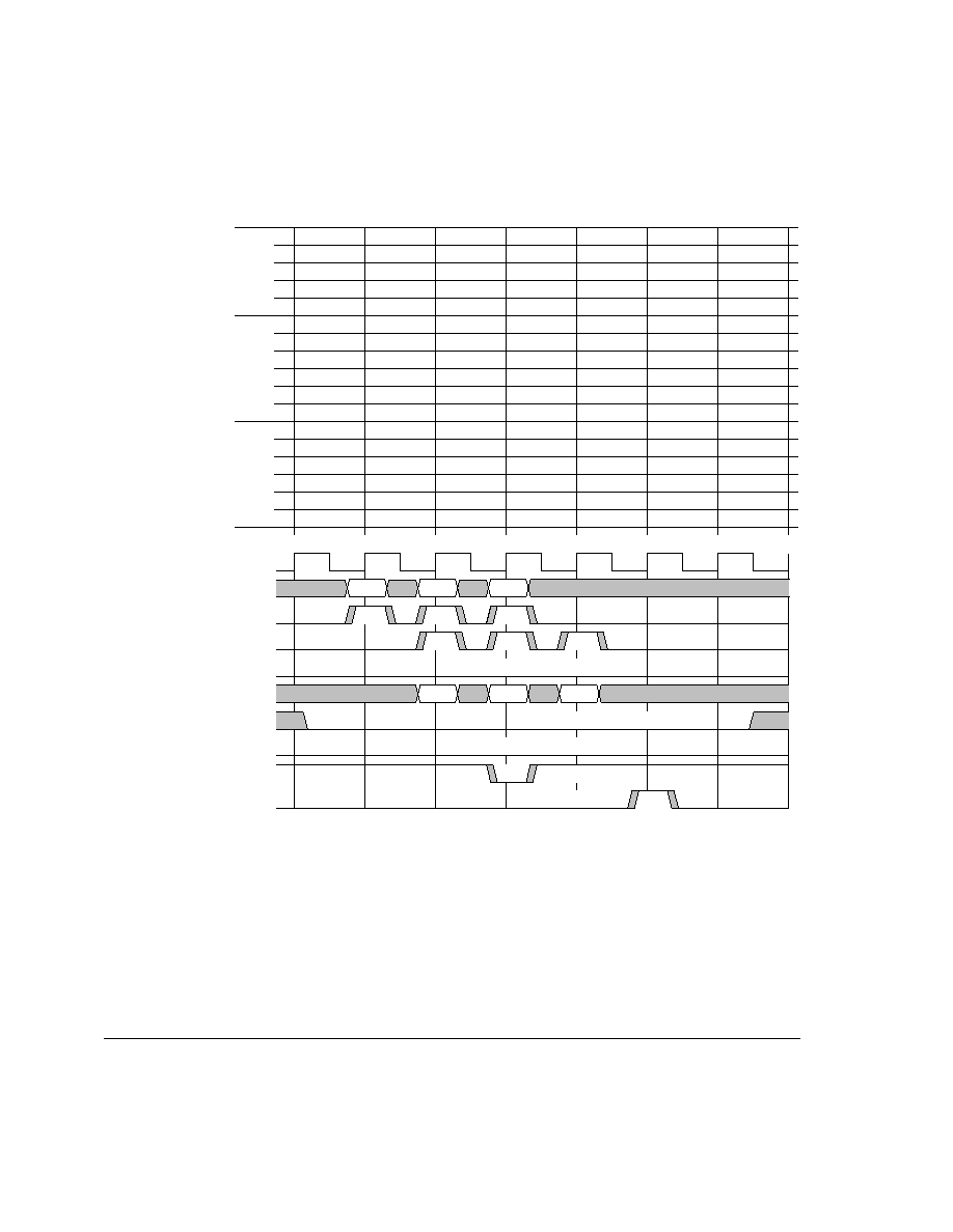
Coprocessor Interface
7-50
Copyright © 2003 ARM Limited. All rights reserved.
ARM DDI 0244C
Figure 7-21 CPBOUNCEE example
The flush can occur for a number of reasons. The undefined instruction trap is a low
priority exception.
2
I1
I1
I2
I1
I1
I2
I1
I2
I3
I
D
E
M
W
F
I
M
W
F
I
M
W
I1
I1
I1
I1
I2
I3
I3
[I3]
ARM
CP1
CP2
D
E
D
E
T1
T2
T3
T4
T5
T6
T7
1
2
2
1
2
1
1
2
1
1
2
CPINSTR
CPINSTRV
CPCLK
CPVALIDD
ASTOPCPD
ASTOPCPE
CPBOUNCEE
AFLUSHCP
2
1
CPLSLEN/SWP/DBL
CPBUSYE
1
2
1
3
2
T8
3
3
3
I3
I1
I2
I2
[I2]
[I3]
[I2]
I1
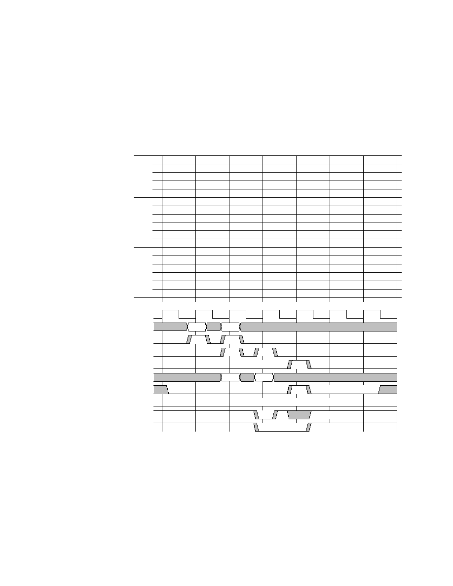
Coprocessor Interface
ARM DDI 0244C
Copyright © 2003 ARM Limited. All rights reserved.
7-51
7.10.3
CPBOUNCEE with ASTOPCPE
In Figure 7-22, instruction 1 is held in the ARM1026EJ-S Execute stage for one cycle.
CPBOUNCEE is considered valid only in the cycle in which ASTOPCPE is
deasserted. So, in this case, instruction 1 does not bounce, and instruction 2 does.
Figure 7-22 CPBOUNCEE with ASTOPCPE example
2
I1
I1
I2
I1
I1
I2
I1
I1
I2
I
D
E
M
W
F
I
M
W
F
I
M
W
I1
I1
I1
I2
I2
ARM
CP1
CP2
D
E
D
E
T1
T2
T3
T4
T5
T6
T7
1
2
2
1
2
1
1
2
1
1
2
CPINSTR
CPINSTRV
CPCLK
CPVALIDD
ASTOPCPD
ASTOPCPE
CPBOUNCEE
CPBOUNCEE (internal)
2
1
CPLSLEN/SWP/DBL
CPBUSYE
1
2
1
1
T8
I2
I2
I2
I1
I1
1
2
1
I2
I1
I1
I2
I2
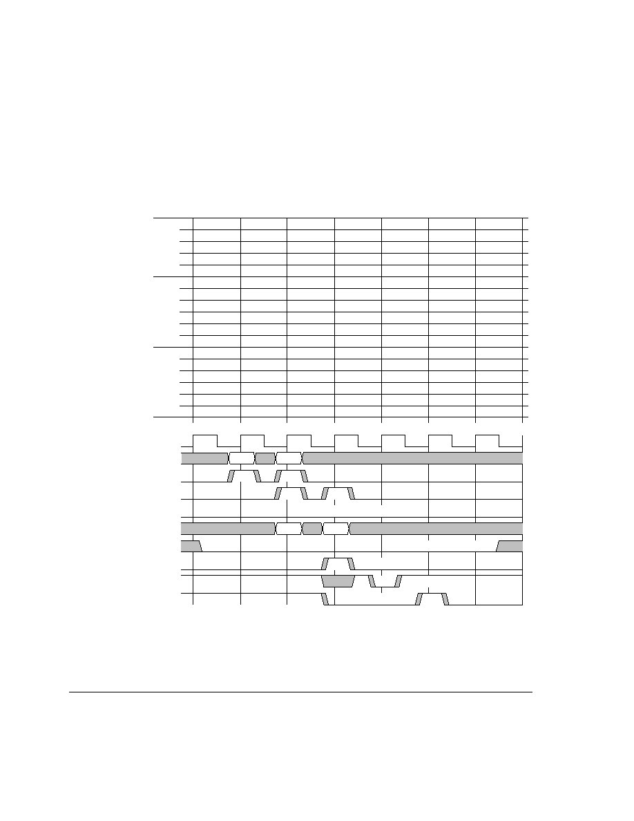
Coprocessor Interface
7-52
Copyright © 2003 ARM Limited. All rights reserved.
ARM DDI 0244C
7.10.4
CPBOUNCEE with CPBUSYE
In Figure 7-23, instruction 1 is held in the ARM1026EJ-S Execute stage for one cycle.
CPBOUNCEE is considered valid only in the cycle in which CPBUSYE is deasserted.
In this case, instruction 1 does not bounce, and instruction 2 does.
Figure 7-23 CPBOUNCEE with CPBUSYE example
I1
I1
I2
I1
I1
I2
I1
I1
I2
I
D
E
M
W
F
I
M
W
F
I
M
W
I1
I1
I1
I2
I2
ARM
CP1
CP2
D
E
D
E
T1
T2
T3
T4
T5
T6
T7
1
2
2
1
2
1
2
1
2
CPINSTR
CPINSTRV
CPCLK
CPVALIDD
ASTOPCPD
ASTOPCPE
CPBOUNCEE
CPBOUNCEE (internal)
2
1
CPLSLEN/SWP/DBL
CPBUSYE
1
2
1
1
T8
I2
I2
I2
I1
I1
1
I2
I1
I1
I2
I2
1
1
1
2

Coprocessor Interface
ARM DDI 0244C
Copyright © 2003 ARM Limited. All rights reserved.
7-53
7.11
Data buses
This section describes the 64-bit data buses:
∑
STCMRCDATA
∑
LDCMCRDATA on page 7-54.
7.11.1
STCMRCDATA
The 64-bit STCMRCDATA bus carries data from a CP to the ARM1026EJ-S
processor. For a data transfer from a CP register to an ARM1026EJ-S register (MRC),
the data on STCMRCDATA is written into a register in the ARM1026EJ-S register
file. For a CP store to memory (STC), the data on STCMRCDATA is passed though
ARM1026EJ-S processor to the memory system. It is stored at an address generated by
the ARM1026EJ-S processor. Table 7-18 describes the interactions between
STCMRCDATA and signals.
STCMRCDATA is driven by a CP in the ARM1026EJ-S Execute stage.
Table 7-18 STCMRCDATA interactions with signals
Signal
Interactions with STCMRCDATA
ASTOPCPD
None.
ASTOPCPE
The ARM1026EJ-S processor registers the value on STCMRCDATA
when ASTOPCPE is asserted and the LSU pipeline and ALU pipeline are
in lockstep. If the pipelines are decoupled, then ASTOPCPE only affects
the data processing operation that might be running under the loads or
stores.
LSHOLDCPE
If the ALU and LSU pipelines are decoupled then ARM1026EJ-S
processor registers the value on STCMRCDATA when LSHOLDCPE is
asserted.
CPBUSYE
None.
LSHOLDCPM
None.
ACANCELCP
None.
CPBOUNCEE
None.

Coprocessor Interface
7-54
Copyright © 2003 ARM Limited. All rights reserved.
ARM DDI 0244C
7.11.2
LDCMCRDATA
The 64-bit LDCMCRDATA bus carries data from the ARM1026EJ-S processor to a
CP. For a data transfer from an ARM1026EJ-S register to a CP register (MCR), the data
on LDCMCRDATA is written into a register in the CP register file. For a CP load from
memory (LDC), the data on LDCMCRDATA is passed though the ARM1026EJ-S
processor from the memory system. It is loaded from an address generated by the
ARM1026EJ-S processor. Table 7-19 shows the interactions of LDCMRCDATA with
other signals.
LDCMRCDATA is driven by the ARM1026EJ-S processor in the ARM1026EJ-S
Write stage.
Table 7-19 LDCMRCDATA interactions with signals
Signal
Interactions with LDCMRCDATA
ASTOPCPD
None.
ASTOPCPE
None.
LSHOLDCPE
None.
CPBUSYE
None.
LSHOLDCPM
LSHOLDCPM indicates that the memory system did not return valid data
in the previous cycle. In this case there is not valid data on
LDCMCRDATA until LSHOLDCPM goes LOW.
ACANCELCP
None.
CPBOUNCEE
None.

ARM DDI 0244C
Copyright © 2003 ARM Limited. All rights reserved.
8-1
Chapter 8
Debug
This chapter describes the debug unit. These features assist the development of
application software, operating systems, and hardware. This chapter contains the
following sections:
∑
About the debug unit on page 8-2
∑
Register descriptions on page 8-6
∑
Software lockout function on page 8-18
∑
Halt mode on page 8-19
∑
Monitor mode on page 8-22
∑
Values in the link register after exceptions on page 8-24
∑
Comms channel on page 8-25.

Debug
8-2
Copyright © 2003 ARM Limited. All rights reserved.
ARM DDI 0244C
8.1
About the debug unit
The ARM1026EJ-S debug unit assists in debugging software running on the
ARM1026EJ-S processor. The debug hardware, in combination with a software
debugger program, can be used to debug:
∑
application software
∑
operating systems
∑
ARM1026EJ-S-based hardware systems.
The debug unit enables you to:
∑
stop program execution
∑
examine and alter processor and coprocessor state
∑
examine and alter memory and input/output peripheral state
∑
restart the processor.
The debug unit provides several ways to stop execution. The most common is for
execution to halt when a particular memory address is accessed, either for an instruction
fetch (a breakpoint), or a data access (a watchpoint). When execution has stopped, one
of two modes is entered:
Halt mode
All processor execution halts, and can only be restarted with
hardware connected to the DBGTAP controller interface. You can
examine and alter all processor state (CPU registers), coprocessor
state, memory, and input/output locations through the DBGTAP
interface. This mode is intentionally invasive to program
execution. In halt mode you can debug the processor irrespective
of its internal state. Halt mode requires external hardware to
control the DBGTAP interface. A software debugger provides the
user interface to the debug hardware.
Monitor mode
In monitor mode the processor stops execution of the current
program and starts execution of a Debug Abort handler. The state
of the processor is preserved in the same manner as all ARM
exceptions (see The ARM Architecture Reference Manual on
exceptions and exception priorities). The abort handler
communicates with a debugger application to access processor
and coprocessor state, and to access memory contents and
input/output peripherals. Monitor mode requires a debug monitor
program to interface between the debug hardware and the
software debugger.

Debug
ARM DDI 0244C
Copyright © 2003 ARM Limited. All rights reserved.
8-3
The ARM1026EJ-S debug interface is based on the IEEE Standard, Test Access Port
and Boundary-Scan Architecture specification. However, the only expected use of this
interface is to access the ARM1026EJ-S debug resources, Therefore, the term Debug
Test Access Port (DBGTAP) is used instead of Test Access Port (TAP), DBGTDI
instead of TDI, and so on. For more information about the Debug Test Access Port used
in an ARM1026EJ-S debug system, see Chapter 9 Debug Test Access Port.
8.1.1
Halt mode and monitor mode compared
Halt mode is for nonreal-time debugging. Because of its hardware nature, you can use
halt mode to debug the processor under almost all circumstances. However, real-time
systems in which processor execution cannot be completely suspended are unlikely to
be able to tolerate the intrusion caused by halt mode. Therefore monitor mode is
provided for time-critical applications that cannot tolerate a long interruption while the
processor is halted. Monitor mode relies on the processor being able to freely execute
instructions to process debug requests.
8.1.2
Programming the debug unit
The debug unit is programmed using coprocessor 14, CP14. CP14 provides:
∑
instruction address comparators for triggering breakpoints
∑
data address comparators for triggering watchpoints
∑
a bidirectional serial communication channel
∑
all other state information associated with debug.
CP14 is accessed using coprocessor instructions in both halt mode and monitor mode.
BKPT instructions cause a Prefetch Abort if debug is disabled.

Debug
8-4
Copyright © 2003 ARM Limited. All rights reserved.
ARM DDI 0244C
8.1.3
Summary of CP14 registers
All debug state is mapped into CP14 as registers. Three CP14 registers, c0, c1, and c5,
can be accessed by software running on the processor. Four registers, c0, c1, c4, and c5,
are accessible as scan chains from the DBGTAP interface. The Instruction Transfer
Register, CP14 c4, is accessible only as a scan chain. The remaining registers are
accessible only by software operating in a privileged processor mode. Table 8-1 shows
the CP14 registers and their scan chain numbers.
The register file has space reserved for up to 16 breakpoints and 16 watchpoints. A
particular implementation can have any number from 2 to 16. The processor has six
instruction-side breakpoints and two data-side watchpoints.
Table 8-1 CP14 registers and scan chain numbers
Register
Name
Scan chain number
CP14 c0
Debug ID Register, DIDR
0
CP14 c1
Debug Status and Control Register, DSCR
1
CP14 c2 and c3
Reserved
-
CP14 c4
Instruction Transfer Register, ITR
4
CP14 c5
Data Transfer Register, DTR
5
CP14 c6-c63
Reserved
-
CP14 c64-c69
Breakpoint Address Registers, BA0-BA5
-
CP14 c70-c79
Reserved
-
CP14 c80-c85
Breakpoint Control Registers, BC0-BC5
-
CP14 c86-c95
Reserved
-
CP14 c96 and c97
Watchpoint Address Registers, WA0 and WA1
-
CP14 c112 and c113
Watchpoint Control Registers, WC0 and WC1
-
CP14 c114 and c127
Reserved
-

Debug
ARM DDI 0244C
Copyright © 2003 ARM Limited. All rights reserved.
8-5
There are two requirements to enable debugging:
∑
An enable bit in the Debug Status and Control Register enables debug
functionality through software. Reset clears the enable bit, disabling all debug
functionality. The processor ignores external debug requests, and BKPT
instructions cause Prefetch Aborts. In this mode, an operating system can quickly
enable and disable debugging on individual tasks as part of the task-switching
sequence.
∑
The DBGEN pin allows the debug features of the processor to be disabled
entirely.
The DBGEN pin must be tied HIGH to enable the debug functionality of the core.
DBGEN must be tied LOW only when debugging is not required.
The CRm and opcode2 fields are used to encode the debug register number, where the
register number is {opcode2, CRm}.

Debug
8-6
Copyright © 2003 ARM Limited. All rights reserved.
ARM DDI 0244C
8.2
Register descriptions
This section describes the CP14 registers:
∑
CP14 c0, Debug ID Register
∑
CP14 c1, Debug Status and Control Register on page 8-7
∑
CP14 c2-c4 on page 8-11
∑
CP14 c5, Data Transfer Register on page 8-11
∑
CP14 c6-c63 on page 8-12
∑
CP14 c64-c69, Breakpoint Address Registers on page 8-12
∑
CP14 c70-c79 on page 8-12
∑
CP14 c80-c85, Breakpoint Control Registers on page 8-13
∑
CP14 c86-c95 on page 8-14
∑
CP14 c96 and c97, Watchpoint Address Registers on page 8-15
∑
CP14 c112 and c113, Watchpoint Control Registers on page 8-15
∑
CP14 c114-c127 on page 8-17.
8.2.1
CP14 c0, Debug ID Register
The Debug ID Register, DIDR, is read-only and contains
0x41016201
. Table 8-2 shows
the instructions for reading DIDR.
Figure 8-1 shows the DIDR bit fields.
Figure 8-1 Debug ID Register
Table 8-2 Debug ID Register instructions
Instruction
Description
MRC p14, 0, Rd, c0, c0, 0
Copies contents of Debug ID Register into Rd.
31
24
15
12
7
4 3
0
Revision
0001
SBZ
0000
Watchpoints
0010
Breakpoints
0110
SBZ
0000
Architecture
0001
Designer code
0100 0001
23
20 19
16
11
8

Debug
ARM DDI 0244C
Copyright © 2003 ARM Limited. All rights reserved.
8-7
Table 8-3 describes the DIDR bit fields.
8.2.2
CP14 c1, Debug Status and Control Register
The Debug Status and Control Register, DSCR, is a read/write register. Table 8-4
shows the instructions for accessing DSCR.
Figure 8-2 on page 8-8 shows the DSCR bit fields.
Table 8-3 Encoding of the Debug ID Register
Bit
Name
Definition
[31:24]
Designer code
Designer code
[23:20]
-
Should Be Zero
[19:16]
Architecture
Debug architecture version
[15:12]
Breakpoints
Number of implemented register breakpoints
[11:8]
Watchpoints
Number of implemented watchpoints
[7:4]
-
Should Be Zero
[3:0]
Revision
Revision number
Table 8-4 Debug Status and Control Register instructions
Instruction
Description
MRC p14, 0, Rd, c0, c1, 0
Copies contents of Debug Status and Control Register into Rd
MCR p14, 0, Rd, c0, c1, 0
Copies contents of Rd into Debug Status and Control Register
Debug
8-8
Copyright © 2003 ARM Limited. All rights reserved.
ARM DDI 0244C
Figure 8-2 Debug Status and Control Register
Table 8-5 describes the DSCR bit fields.
31 30
1 0
CF
C1
Reserved
GE
MOE
CR
CP
CS
CU
R
CD
RF
WE
2
4
HLT
C
RS
29 28 27
24 23 22 21 20 19 18 17 16
H E T
Reserved
7 6 5
A
15
8
26
Table 8-5 Encoding of Debug Status and Control Register
Bit
Name
Definition
[31]
GE
Global debug enable bit:
1 = all debugging functions enabled
0 = all debugging functions disabled.
Reset clears GE.
[30]
H
Halt mode bit:
1 = halt mode
0 = monitor mode.
Reset clears H.
[29]
E
Execute instruction in ITR select:
1 = execute instruction in ITR when DBGTAP is in Run-Test/Idle state
0 = do not execute instruction in ITR when in DBGTAP is in Run-Test/Idle state.
[28]
T
Thumb instruction bit:
1 = ITR contains a Thumb instruction
0 = ITR contains an ARM instruction.
[27]
C
Comms channel mode:
1 = comms channel activity
0 = no comms channel activity.
[26:24]
-
Reserved.

Debug
ARM DDI 0244C
Copyright © 2003 ARM Limited. All rights reserved.
8-9
DSCR[23:22] and DSCR[20:16] are used to catch ARM exceptions. The effect of setting one of these bits
is the same as setting a register breakpoint on the address of the exception vector.
[23]
CF
Vector catch FIQ bit.
[22]
CI
Vector catch IRQ bit.
[21]
-
Reserved.
[20]
CD
Vector catch Data Abort bit.
[19]
CP
Vector catch Prefetch Abort bit.
[18]
CS
Vector catch Software Interrupt bit.
[17]
CU
Vector catch Undefined Instruction bit.
[16]
CR
Vector catch reset bit.
[15:8]
-
Reserved.
[7]
RF
rDTR buffer full bit:
1 = new DBGTAP controller data readable with MRC or STC present in the rDTR
0 = no new DBGTAP controller data in rDTR.
RF indicates to the processor that the rDTR buffer is full of data written by the
debugger. RF is the inversion of the bit that the DBGTAP debugger sees when it
polls the DTR by going through Capture-DR state with INTEST. Because the timing
of the DBGTAP controller and processor can be different, the debugger must not use
RF to determine if the rDTR is empty or full.
[6]
WE
wDTR buffer empty bit:
1 = wDTR ready for new data
0 = unread data in wDTR.
WE indicates to the processor that the wDTR buffer is empty and that the processor
can write more data into it. WE is the inversion of the bit that the DBGTAP
debugger sees when it polls the DTR by going through Capture-DR state with
EXTEST. Because the timing of the DBGTAP controller and the processor can be
different, the debugger must not use WE to determine if the wDTR is empty or full.
[5]
A
Sticky abort flag:
1 = abort occurred after last time A was cleared
0 = no abort occurred after last time A was cleared.
This bit is cleared when the DBGTAP debugger reads the DSCR.
Table 8-5 Encoding of Debug Status and Control Register (continued)
Bit
Name
Definition

Debug
8-10
Copyright © 2003 ARM Limited. All rights reserved.
ARM DDI 0244C
The DSCR can be seen from processor and from the DBGTAP debugger. Table 8-6
summarizes the accessibility of the DSCR bits as seen from the processor and the
DBGTAP debugger.
[4:2]
MOE
Method of entry bits:
b000 = DBGTAP HALT instruction
b001 = breakpoint hit
b010 = watchpoint hit
b011 = breakpoint instruction requested
b100 = external debug requested asserted
b101 = vector catch occurred
b110 = data-side abort occurred
b111 = instruction-side abort occurred.
[1]
RS
Core restarted flag:
1 = processor has exited debug state
0 = processor is exiting debug state.
The DBGTAP debugger can poll this bit to determine when the processor has exited
debug state.
[0]
HLT
Core halted flag:
1 = processor is in debug state
0 = processor is in normal state.
The DBGTAP debugger can poll this bit to determine when the processor has
entered debug state.
Table 8-5 Encoding of Debug Status and Control Register (continued)
Bit
Name
Definition
Table 8-6 DSCR bits from the core
DSCR bits
View from core
View from debugger
[1:0]
Reserved
Read-only
[4:2]
Read-only
Read-only
[5]
Reserved
Read-only
[7:6]
Read-only
Read-only
[15:8]
Reserved
Reserved
[23:22]
Read-only
Read/write
[21]
Reserved
Reserved
[20:16]
Read-only
Read/write

Debug
ARM DDI 0244C
Copyright © 2003 ARM Limited. All rights reserved.
8-11
8.2.3
CP14 c2-c4
CP14 c2-c4 are reserved.
8.2.4
CP14 c5, Data Transfer Register
The Data Transfer Register, DTR, is a read/write register. Table 8-7 shows the
instructions for accessing DTR.
Figure 8-3 shows the DTR bit field.
Figure 8-3 Data Transfer Register
Note
Physically, the DTR is two separate registers, the rDTR for reading and the wDTR for
writing.
[26:24]
Reserved
Reserved
[30:27]
Reserved
Read/write
[31]
Read/write
Read-only
Table 8-6 DSCR bits from the core
DSCR bits
View from core
View from debugger
Table 8-7 Data Transfer Register instructions
Instruction
Description
MRC p14, 0, Rd, c0, c5, 0
Copies contents of DTR into Rd
MCR p14, 0, Rd, c0, c5, 0
Copies contents of Rd into DTR
LDC p14, c5, <addressing mode>
Loads value accessed in memory into DTR
STC p14, c5, <addressing mode>
Stores contents of DTR to memory
31
0
Transfer data

Debug
8-12
Copyright © 2003 ARM Limited. All rights reserved.
ARM DDI 0244C
8.2.5
CP14 c6-c63
CP14 c6-c63 are reserved.
8.2.6
CP14 c64-c69, Breakpoint Address Registers
The Breakpoint Address Registers, BA0-5, are read/write registers. Table 8-8 shows the
instructions for accessing BA0-5.
Figure 8-4 shows the BA0-5 bit field.
Figure 8-4 Breakpoint Address Registers
8.2.7
CP14 c70-c79
CP14 c70-c79 are reserved.
Table 8-8 Breakpoint Address Register instructions
Register
Instruction
Description
CP14 c64, BA0
MRC p14, 0, Rd, c0, c0, 4
Copies contents of BA0 into Rd
MCR p14, 0, Rd, c0, c0, 4
Copies contents of Rd into BA0
CP14 c65, BA1
MRC p14, 0, Rd, c0, c1, 4
Copies contents of BA1 into Rd
MCR p14, 0, Rd, c0, c1, 4
Copies contents of Rd into BA1
CP14 c66, BA2
MRC p14, 0, Rd, c0, c2, 4
Copies contents of BA2 into Rd
MCR p14, 0, Rd, c0, c2, 4
Copies contents of Rd into BA2
CP14 c67, BA3
MRC p14, 0, Rd, c0, c3, 4
Copies contents of BA3 into Rd
MCR p14, 0, Rd, c0, c3, 4
Copies contents of Rd into BA3
CP14 c68, BA4
MRC p14, 0, Rd, c0, c4, 4
Copies contents of BA4 into Rd
MCR p14, 0, Rd, c0, c4, 4
Copies contents of Rd into BA4
CP14 c69, BA5
MRC p14, 0, Rd, c0, c5, 4
Copies contents of BA5 into Rd
MCR p14, 0, Rd, c0, c5, 4
Copies contents of Rd into BA5
31
0
Breakpoint address

Debug
ARM DDI 0244C
Copyright © 2003 ARM Limited. All rights reserved.
8-13
8.2.8
CP14 c80-c85, Breakpoint Control Registers
The Breakpoint Control Registers, BC0-5, are read/write registers. Table 8-9 shows the
instructions for accessing BC0-5.
Figure 8-5 shows the BC0-5 bit fields.
Figure 8-5 Breakpoint Control Registers
Table 8-9 Breakpoint Control Register instructions
Register
Instruction
Description
CP14 c80, BC0
MRC p14, 0, Rd, c0, c0, 5
Copies contents of BC0 into Rd
MCR p14, 0, Rd, c0, c0, 5
Copies contents of Rd into BC0
CP14 c81, BC1
MRC p14, 0, Rd, c0, c1, 5
Copies contents of BC1 into Rd
MCR p14, 0, Rd, c0, c1, 5
Copies contents of Rd into BC1
CP14 c82, BC2
MRC p14, 0, Rd, c0, c2, 5
Copies contents of BC2 into Rd
MCR p14, 0, Rd, c0, c2, 5
Copies contents of Rd into BC2
CP14 c83, BC3
MRC p14, 0, Rd, c0, c3, 5
Copies contents of BC3 into Rd
MCR p14, 0, Rd, c0, c3, 5
Copies contents of Rd into BC3
CP14 c84, BC4
MRC p14, 0, Rd, c0, c4, 5
Copies contents of BC4 into Rd
MCR p14, 0, Rd, c0, c4, 5
Copies contents of Rd into BC4
CP14 c85, BC5
MRC p14, 0, Rd, c0, c5, 5
Copies contents of BC5 into Rd
MCR p14, 0, Rd, c0, c5, 5
Copies contents of Rd into BC5
E
0
SA
IT
SBZ
31
5 4 3 2 1

Debug
8-14
Copyright © 2003 ARM Limited. All rights reserved.
ARM DDI 0244C
Table 8-10 describes the BC0-5 bit fields.
8.2.9
CP14 c86-c95
CP14 c86-c95 are reserved.
Table 8-10 Encoding of Breakpoint Control Registers
Bit
Name
Definition
[31:5]
-
Should Be Zero.
[5:3]
IT
Instruction type bits:
b000 = reserved
b1xx = Jazelle instruction
bx1x = ARM instruction
bxx1 = Thumb instruction
b111 = Jazelle or ARM or Thumb
instruction.
[2:1]
SA
Supervisor access bits:
b00 = reserved
b10 = privileged
b01 = user
b11 = either.
[0]
E
Enable bit:
1 = register enabled
0 = register disabled.
Reset clears E.

Debug
ARM DDI 0244C
Copyright © 2003 ARM Limited. All rights reserved.
8-15
8.2.10
CP14 c96 and c97, Watchpoint Address Registers
The Watchpoint Address Registers, WA0 and WA1, are read/write registers. Table 8-11
shows the instructions for accessing WA0 and WA1.
Figure 8-6 shows the watchpoint address bit field.
Figure 8-6 Watchpoint Address Registers
8.2.11
CP14 c112 and c113, Watchpoint Control Registers
The Watchpoint Control Registers, WC0 and WC1, are read/write registers. Table 8-12
shows the instructions for accessing WC0 and WC1.
Figure 8-7 on page 8-16 shows the WC0 and WC1 bit fields.
Table 8-11 Watchpoint Address Register instructions
Register
Instruction
Description
CP14 c96, WA0
MRC p14, 0, Rd, c0, c0, 6
Copies contents of WA0 into Rd
MCR p14, 0, Rd, c0, c0, 6
Copies contents of Rd into WA0
CP14 c97, WA1
MRC p14, 0, Rd, c0, c1, 6
Copies contents of WA1 into Rd
MCR p14, 0, Rd, c0, c1, 6
Copies contents of Rd into WA1
31
0
Watchpoint address
Table 8-12 Watchpoint Control Register instructions
Register
Instruction
Description
CP14 c112, WC0
MRC p14, 0, Rd, c0, c0, 7
Copies contents of WC0 into Rd
MCR p14, 0, Rd, c0, c0, 7
Copies contents of Rd into WC0 control
CP14 c113, WC1
MRC p14, 0, Rd, c0, c1, 7
Copies contents of WC1 into Rd
MCR p14, 0, Rd, c0, c1, 7
Copies contents of Rd into WC1

Debug
8-16
Copyright © 2003 ARM Limited. All rights reserved.
ARM DDI 0244C
Figure 8-7 Watchpoint Control Registers
Table 8-13 describes the WC0 and WC1 bit fields.
E
8
0
L/S/E S
Size
Mask
SBZ
7
5 4 3
10 9
2 1
SBZ
31
11
Table 8-13 Encoding of Watchpoint Control Registers
Bit
Name
Definition
[31:11]
-
Should Be Zero.
[10:9]
Mask
DA[1:0] address mask bits.
Bit 10:
1 = exclude DA1 in comparison
0 = include DA1 in comparison.
Bit 9:
1 = exclude DA0 in comparison
0 = include DA0 in comparison.
[8]
-
Should Be Zero.
[7:5]
Size
Size select bits:
b000 = reserved
b001 = byte
b010 = halfword
b011 = byte or halfword
b100 = word
b101 = word or byte
b110 = word or halfword
b111 = any size.

Debug
ARM DDI 0244C
Copyright © 2003 ARM Limited. All rights reserved.
8-17
8.2.12
CP14 c114-c127
CP14 c114-c127 are reserved.
[4:3]
L/S/E
Load/store/either select bits:
b00 = reserved
b10 = load
b01 = store
b11 = either.
[2:1]
S
Supervisor bits:
b00 = reserved
b10 = privileged
b01 = user
b11 = either.
[0]
E
Enable bit:
1 = register enabled
0 = register disabled.
Reset clears E.
Table 8-13 Encoding of Watchpoint Control Registers (continued)
Bit
Name
Definition

Debug
8-18
Copyright © 2003 ARM Limited. All rights reserved.
ARM DDI 0244C
8.3
Software lockout function
When the DBGTAP debugger is attached to an evaluation board or test system, it
indicates its presence by setting the halt/monitor mode bit in the DSCR. When
breakpoint and watchpoint registers have been configured, software cannot alter them
if the halt/monitor mode bit remains set, because the debugger retains control. In this
mode, software can still write to the comms channel register.

Debug
ARM DDI 0244C
Copyright © 2003 ARM Limited. All rights reserved.
8-19
8.4
Halt mode
Halt mode is for debugging the processor using external hardware connected to the
DGBTAP interface. The external hardware provides an interface to a DBGTAP
debugger application. Halt mode can be selected only by setting the H bit (bit 30) of the
DSCR, which is only writable through the DBGTAP interface.
8.4.1
Entering debug state
In halt mode, the processor stops executing instructions and enters into debug state if
one of the following events occurs:
∑
an instruction is fetched from a breakpointed memory location
∑
a data fetch (load or store) occurs from a watchpointed data location
∑
a breakpoint instruction is executed
∑
the external EDBGRQ signal is asserted
∑
a HALT instruction is scanned into the DBGTAP instruction register
∑
an exception occurs and the corresponding vector catch bit is set.
When the processor is halted, it is controlled by sending instructions to the integer unit
through the DBGTAP port. Any valid instruction sequence can be scanned into the
processor, and the effect of the instruction on the integer unit is as if the instruction is
executed under normal operations. Some specific exceptions are described in Sending
instructions to the integer unit on page 8-20 and Using the DSCR E bit for fast data
uploads and downloads on page 8-20. Also accessible through the DBGTAP interface
is a register to transfer data between CP14 and the DBGTAP debugger.
The integer unit is restarted by executing a DBGTAP RESTART instruction.
8.4.2
Exiting debug state
Exiting debug state involves causing a branch to the next instruction to be executed.
If debug state was entered from ARM or Thumb state, the processor typically issues a
load or data processing instruction with PC as destination to exit debug state and
re-enter ARM or Thumb state.
If debug state was entered from Jazelle state, the processor must issue the BXJ Rm
instruction followed by a load or data processing operation with PC as destination to
exit debug state back to Jazelle state.

Debug
8-20
Copyright © 2003 ARM Limited. All rights reserved.
ARM DDI 0244C
8.4.3
Behavior of the PC in debug state
When the processor is halted, the PC is frozen on entry to debug state. The PC is not
incremented as instructions are executed. However, branches and instructions that
modify the PC directly update the PC.
Table 8-14 shows the read PC value after debug state entry for different debug events.
8.4.4
Sending instructions to the integer unit
Two registers in CP14 are used to communicate with the processor:
∑
the Instruction Transfer Register, ITR
∑
the Data Transfer Register, DTR.
The ITR is used to insert an instruction into the processor pipeline. While in debug state,
most of the processor time is spent waiting for a valid instruction in the ITR. Undefined
instructions fed to the integer unit through the debugger are Unpredictable. Instructions
that cause exceptions cause Unpredictable behavior.
8.4.5
Using the DSCR E bit for fast data uploads and downloads
The E bit in the DSCR enables execution of the instruction in the ITR. You can use it
to repeatedly issue instructions to the integer unit. When E is set, the current ITR
instruction is sent to the prefetch unit for execution each time the DBGTAP controller
enters the Run-Test/Idle state. When E is clear, no instruction is passed to the prefetch
unit. The instruction in the DBGTAP instruction register must be either INTEST or
EXTEST.
Table 8-14 Read PC value after debug state entry
Debug event
ARM
Thumb Jazelle Return address (RA
a
) meaning
Register breakpoint
RA + 8 RA + 4
RA
Register breakpoint hit instruction address.
Watchpoint
RA + 8 RA + 4
RA
Address of instruction where execution is expected to resume. Can be
a number of instructions after the watchpointed instruction.
Instruction breakpoint RA + 8 RA + 4
RA
Breakpoint instruction address.
Vector catch
RA + 8 RA + 4
RA
Vector address.
EDBGRQ asserted
RA + 8 RA + 4
RA
Address of instruction where execution is expected to resume.
HALT instruction
RA + 8 RA + 4
RA
Address of instruction where execution is expected to resume.
a. RA is the address of the instruction that the processor should execute first on debug state exit. Watchpoints can be imprecise,
and RA might not be the address of the watchpointed instruction. The processor might stop a number of instructions later.

Debug
ARM DDI 0244C
Copyright © 2003 ARM Limited. All rights reserved.
8-21
The execute feature enables fast uploads and downloads of data. For example, a
download sequence might consist of:
1.
In the Debug Scan Chain Select Register, DBGSCREG, select scan chain 2, the
combination of scan chains 4 and 5, and set the DBGTAP instruction to EXTEST
for writing.
2.
Load an STC instruction into the ITR, and load data into the DTR.
3.
When the DBGTAP controller passes through the Run-Test/Idle state, the
processor executes the instruction in the ITR.
4.
Switch to scan chain 5, the DTR, and poll the DTR until the status bit in wDTR0
indicates the completion of the instruction.
More data can then be loaded into DTR and the instruction reexecuted by passing
through Run-Test/Idle. The STC instruction must specify base address write-back so
that the addresses are automatically updated.
A similar mechanism can increase the performance of upload:
1.
First, change the DBGTAP instruction to EXTEST for writing.
2.
Using scan chain 2, scan a read instruction such as LDC into the ITR.
3.
Change the DBGTAP instruction to INTEST for reading.
4.
Switch to scan chain 5, the DTR, and poll the DTR until the instruction
completes. By passing through the Run-Test/Idle state on the way to Shift-DR for
polling, the instruction in the ITR is issued to the integer unit.
Repeat this process until the last word is read.
8.4.6
Accessing processor state
Reading the contents of the integer unit register file requires individual moves from an
ARM1026EJ-S register to CP14 c5 using MRC and MCR instructions. The data is then
scanned out of the DTR.
Byte and halfword transfers are performed by transferring both the address and data into
ARM1026EJ-S registers and then executing the appropriate ARM instructions.
Transfers to and from coprocessors are performed by moving data through an
ARM1026EJ-S register. For this reason all coprocessors must have all data accessible
using MRC and MCR. Otherwise, a data buffer in writable memory must be used.

Debug
8-22
Copyright © 2003 ARM Limited. All rights reserved.
ARM DDI 0244C
8.5
Monitor mode
Monitor mode is useful in real-time systems when the integer unit cannot be halted to
collect information. Engine controllers and servo mechanisms in hard drive controllers
that cannot stop the code without physically damaging the components are examples.
For situations that can only tolerate a small intrusion into the instruction stream,
monitor mode is ideal. Using this technique, code can be suspended with an exception
long enough to save off state information and important variables. The code continues
when the exception handler is finished. The MOE bits in the DSCR can be read to
determine what caused the exception.
8.5.1
Entering monitor mode
Monitor mode is the default mode on Reset. Only an external debugger can change the
mode bit in the DSCR. When monitor mode is enabled, the processor takes an
exception, rather than halting, if one of the following events occurs:
∑
a register breakpoint is hit
∑
a watchpoint is hit
∑
a breakpoint instruction reaches the Execute stage of the ARM1026EJ-S pipeline
∑
an exception is taken and the corresponding vector trap bit is set.
The global debug enable bit in the DSCR must be set or no action is taken.
Watchpoints cause Data Abort exceptions. Register breakpoints and instruction
breakpoints cause Prefetch Abort exceptions.
8.5.2
Exiting monitor mode
Exiting the exception handler must be done in the normal fashion.
For example, if the processor takes an exception on a breakpoint instrution (BKPT for
ARM and Thumb,
0xFF
for Jazelle), the Prefetch Abort exception handler might return
to the instruction following the breakpoint instruction.
For ARM, the following instruction can be used:
MOVS PC, R14
For Thumb, the following instruction can be used:
SUBS PC, R14, #2
For Jazelle, the following instruction can be used:
SUBS PC, R14, #3

Debug
ARM DDI 0244C
Copyright © 2003 ARM Limited. All rights reserved.
8-23
8.5.3
Reading and writing breakpoint and watchpoint registers
When in monitor mode, all breakpoint and watchpoint registers can be read and written
with MRC and MCR instructions from a privileged processing mode.

Debug
8-24
Copyright © 2003 ARM Limited. All rights reserved.
ARM DDI 0244C
8.6
Values in the link register after exceptions
After an exception, r14, the link register, holds an address for exception processing.
This address is used to return after the exception is processed and to address the faulted
instruction. Prefetch Aborts and Data Aborts might not want to rerun the faulted
instruction.
Table 8-15 shows the values in the link register after exceptions.
Table 8-15 Link register values after exceptions
Debug event
ARM
Thumb
Jazelle
Return address (RA
a
) meaning
Register breakpoint
RA + 4
RA + 4
RA + 4
Register breakpoint hit instruction address.
Watchpoint
RA + 8
RA + 8
RA + 8
Address of instruction where execution is expected to resume.
Can be a number of instructions after the watchpointed
instruction.
Instruction breakpoint
RA + 4
RA + 4
RA + 4
Breakpoint instruction address.
Vector catch
RA + 4
RA + 4
RA + 4
Vector address.
Prefetch Abort
RA + 4
RA + 4
RA + 4
Address of instruction where execution is expected to resume.
Data Abort
RA + 8
RA + 8
RA + 8
Address of instruction where execution is expected to resume.
a. RA is the address of the instruction that the processor should execute first on debug state exit. Watchpoints can be imprecise,
and RA might not be the address of the watchpointed instruction. The processor might stop a number of instructions later.

Debug
ARM DDI 0244C
Copyright © 2003 ARM Limited. All rights reserved.
8-25
8.7
Comms channel
The comms channel is implemented using the two physically separate DTRs and a
full/empty bit pair to augment each register, creating a bidirectional data port. One
register, wDTR, can be read from the DBGTAP interface and is written from the
ARM1026EJ-S processor wDTR. The other register, rDTR, is written from the
DBGTAP interface and read by the processor. The full/empty bit pair for each register
is automatically updated by the debug unit hardware, and is accessible to both the
DBGTAP interface and to software running on the processor.
When the debugger performs comms channel activities, it indicates this to the hardware
by setting DSCR27 in scan chain 1. This forces the least significant bit of the wDTR to
indicate the state of the comms channel registers.
To read data from the wDTR, the debugger loads the INTEST instruction into the
DBGTAP instruction register and then scans out the contents of the wDTR register. If
the LSB of the 33-bit packet of data is HIGH, the data is valid. The bit is then cleared
by this read. If the bit is a 0, meaning that the core has not written any data for the
debugger, the external hardware can poll the DSCR to see if the core halted.
To write data into the rDTR, the debugger scans the EXTEST instruction into the
DBGTAP instruction register and then scans data into the rDTR. When the debugger
writes more data, it polls the LSB of the register until the LSB is HIGH. If the LSB is
LOW, indicating the rDTR is still full and the core has not read the old data, then the
new data shifted in is not loaded into the rDTR.
Because halt mode and monitor mode are mutually exclusive, the transfer registers are
not used for any other purpose in monitor mode.
Figure 8-8 on page 8-26 shows the output from the comms channel.

Debug
8-26
Copyright © 2003 ARM Limited. All rights reserved.
ARM DDI 0244C
Figure 8-8 Comms channel output
rDTR empty
wDTR full
32
1
Write data from
ARM1026EJ-S
processor
wDTR
32
1
Read data to
ARM1026EJ-S
processor
rDTR
0
DBGTDO
DBGTDI

ARM DDI 0244C
Copyright © 2003 ARM Limited. All rights reserved.
9-1
Chapter 9
Debug Test Access Port
This chapter describes the JTAG interface built into the ARM1026EJ-S processor. It
contains the following sections:
∑
Debug test access port and halt mode on page 9-2
∑
DBGTAP instructions on page 9-4
∑
Scan chain descriptions on page 9-7.
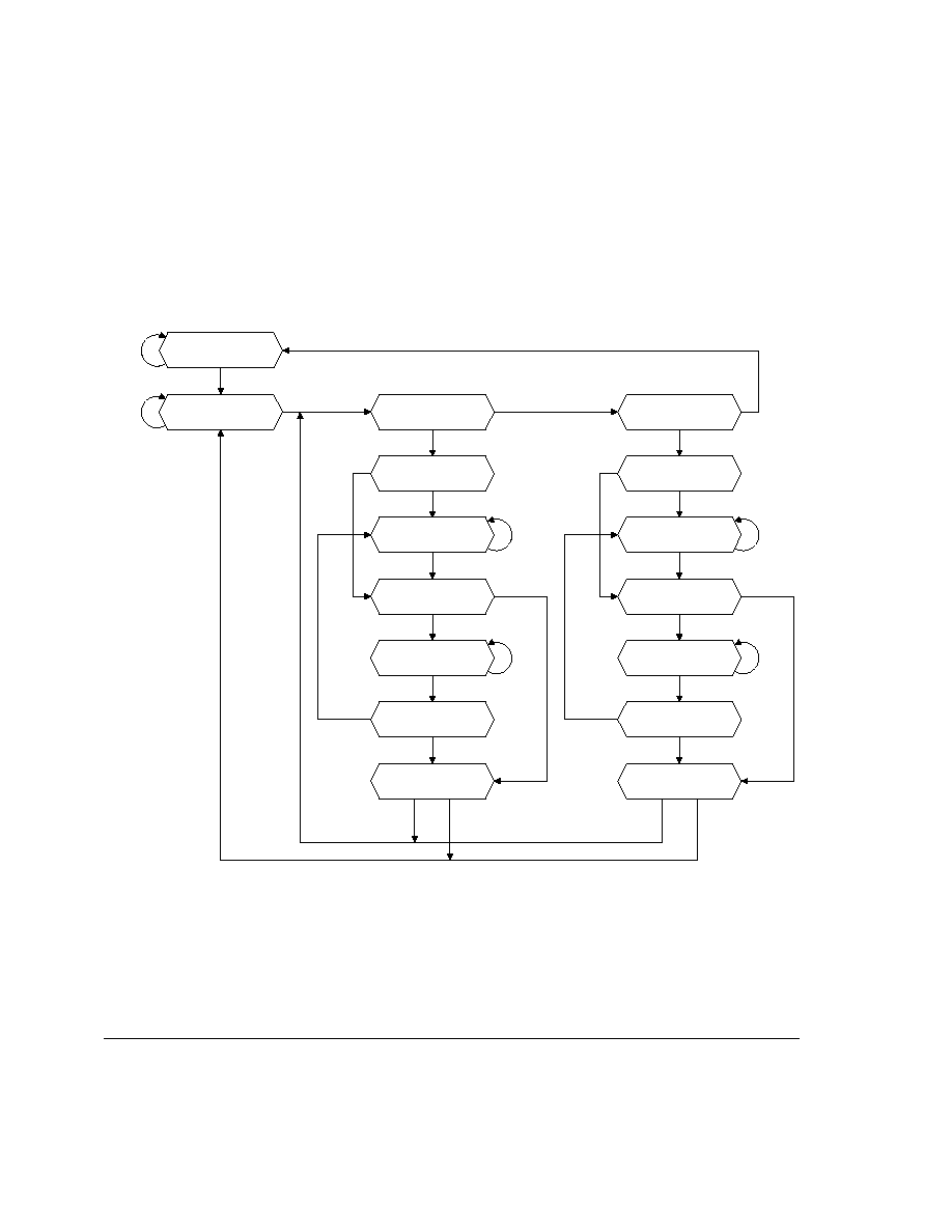
Debug Test Access Port
9-2
Copyright © 2003 ARM Limited. All rights reserved.
ARM DDI 0244C
9.1
Debug test access port and halt mode
JTAG-based hardware debug using halt mode provides access to the integer unit and
debug logic. Access is through scan chains and the ARM1026EJ-S DBGTAP
controller. Figure 9-1 shows the transitions of the DBGTAP state machine.
Figure 9-1 JTAG DBGTAP state diagram
tms = 0
tms = 1
Test-Logic-Reset
0xF
tms = 0
Run-Test/Idle
0xC
Select-DR-Scan
0x7
Capture-DR
0x6
tms = 1
tms = 0
Shift-DR
0x2
tms = 0
Exit1-DR
0x1
tms = 1
tms = 0
Pause-DR
0x3
tms = 1
Exit2-DR
0x0
tms = 1
Update-DR
0x5
tms = 1
tms = 0
tms = 0
tms = 0
tms = 1
tms = 0
tms = 1
Select-IR-Scan
0x4
Capture-IR
0xE
Shift-IR
0xA
Exit1-IR
0x9
Pause-IR
0xB
Exit2-IR
0x8
Update-IR
0xD
tms = 1
tms = 0
tms = 0
tms = 0
tms = 0
tms = 1
tms = 1
tms = 1
tms = 1
tms = 1
tms = 0
tms = 1
tms = 0
tms = 1
tms = 1

Debug Test Access Port
ARM DDI 0244C
Copyright © 2003 ARM Limited. All rights reserved.
9-3
9.1.1
Entering debug state
Halt mode is enabled by writing a 1 to bit 30 of the Debug Status and Control Register,
DSCR. This can only be done by DBGTAP debugger hardware such as Multi-ICE. If
one of the following events occurs when halt mode is enabled, the processor halts and
enters into debug state instead of taking an exception in software:
∑
A HALT instruction is scanned in through the DBGTAP. The DBGTAP
controller must pass through Run-Test/Idle to issue the HALT instruction to the
ARM1026EJ-S processor.
∑
An vector catch occurs, and the corresponding vector catch enable bit is set.
∑
A register breakpoint hits.
∑
A watchpoint hits.
∑
A breakpoint instruction reaches the Execute stage of the ARM1026EJ-S
pipeline.
∑
EDBGRQ is asserted.
The core halted bit in the DSCR is set when debug state is entered. At this point, the
debugger determines why the processor is halted and preserves the processor state. The
MSR instruction can be used to change modes and gain access to all banked registers in
the processor. While in debug state:
∑
the PC is not incremented
∑
external interrupts are ignored
∑
all instructions are read from scan chain 4, the Instruction Transfer Register, ITR.
9.1.2
Exiting debug state
To exit from debug state, scan in the RESTART instruction through the DBGTAP. The
debugger might adjust the PC before restarting, depending on the way the processor
entered debug state. When the state machine enters the Run-Test/Idle state, normal
operations resume. The delay, waiting until the state machine is in Run-Test/Idle,
enables conditions to be set up in other devices in a multiprocessor system without
taking immediate effect. When Run-Test/Idle state is entered, all the processors resume
operation simultaneously. The core restarted bit, DSCR1, is set when the RESTART
sequence is complete.The core halted bit, DSCR0, is cleared before the processor is
restarted.

Debug Test Access Port
9-4
Copyright © 2003 ARM Limited. All rights reserved.
ARM DDI 0244C
9.2
DBGTAP instructions
The ARM1026EJ-S DBGTAP controller is part of the debug logic that enables access
through the DBGTAP to the on-chip debug resources, such as breakpoint and
watchpoint registers. The DBGTAP controller is based on the IEEE 1149.1 standard
and supports:
∑
a TAP ID Register
∑
a Bypass Register
∑
a four-bit Instruction Register, DBGIR
∑
a five-bit Scan Chain Select Register, DBGSCREG.
In addition, the public instructions listed in Table 9-1 are supported.
Table 9-1 Supported public JTAG instructions
Binary code
Instruction
Description
b0000
EXTEST
See Scan chains on page 9-6
b0001
-
Reserved
b0010
SCAN_N
Selects the DBGSCREG
b0011
-
Reserved
b0100
RESTART
Forces the processor to leave debug state
b0101
-
Reserved
b0110
-
Reserved
b0111
-
Reserved
b1000
HALT
Forces the processor to enter debug state
b1001
-
Reserved
b1010-b1011
-
Reserved
b1100
INTEST
See Scan chains on page 9-6
b1101
-
Reserved
b1110
IDCODE
Selects DBGTAP controller TAP ID Register
b1111
BYPASS
Selects DBGTAP controller Bypass Register

Debug Test Access Port
ARM DDI 0244C
Copyright © 2003 ARM Limited. All rights reserved.
9-5
Note
Because the ARM1026EJ-S DBGTAP does not support the attachment of external
boundary scan chains, the SAMPLE/PRELOAD, CLAMP, HIGHZ, and CLAMPZ
instructions are not implemented.
All unused DBGTAP controller instructions default to the BYPASS instruction.
9.2.1
EXTEST
This instruction connects the selected scan chain between DBGTDI and DBGTDO.
When the DBGIR is loaded with the EXTEST instruction, the debug scan chains can be
written.
CP14 debug registers that can be written through the DBGTAP controller, c1, c4, and
c5, are written using an EXTEST instruction.
9.2.2
SCAN_N
This instruction connects the DBGSCREG between DBGTDI and DBGTDO. See
Debug Scan Chain Select Register, DBGSCREG on page 9-9.
9.2.3
RESTART
This instruction is used to exit from debug state. The processor restarts when the
Run-Test/Idle state is entered.
9.2.4
HALT
This instruction stops the processor and puts it into debug state. The processor can be
put into debug state only if debug halt mode is enabled.
9.2.5
INTEST
This instruction connects the selected scan chain between DBGTDI and DBGTDO.
When the DBGIR is loaded with the INTEST instruction, the debug scan chains can be
read.
CP14 debug registers c0, c1, and c5 can be read through the DBGTAP controller using
an INTEST instruction.

Debug Test Access Port
9-6
Copyright © 2003 ARM Limited. All rights reserved.
ARM DDI 0244C
9.2.6
IDCODE
This instruction connects the TAP ID Register between DBGTDI and DBGTDO. The
32-bit TAP ID Register enables the manufacturer, part number, and version of a
component to be determined through the DBGTAP controller.
9.2.7
BYPASS
This instruction connects a one-bit shift register, the Bypass Register, between
DBGTDI and DBGTDO. The first bit shifted out is a zero. All unused DBGTAP
controller instructions default to the BYPASS instruction.
9.2.8
Scan chains
The effect of an INTEST or EXTEST instruction is as follows:
1.
Load the SCAN_N instruction into the DBGIR. Now DBGSCREG is selected
between DBGTDI and DBGTDO.
2.
Load the number of the required scan chain. For example, load the binary value
b00101 to access scan chain 5, the Data Transfer Register.
3.
Load either INTEST or EXTEST into the DBGIR.
4.
Go through the DR leg of the DBGTAPSM to access the scan chain.
INTEST and EXTEST must be used as follows:
INTEST
Use INTEST for reading the active scan chain. Data is
captured into the shift register in the capture-DR state. The
previous value of the scan chain is shifted out during the
Shift-DR state, while a new value is shifted in. The scan
chain is not updated during Update-DR.
EXTEST
Use EXTEST for writing the active scan chain. Data is
captured into the shift register in the Capture-DR state. The
previous value of the scan chain is shifted out during the
Shift-DR state, while a new value is shifted in. The scan
chain is updated with the new value during Update-DR.

Debug Test Access Port
ARM DDI 0244C
Copyright © 2003 ARM Limited. All rights reserved.
9-7
9.3
Scan chain descriptions
This section describes the following scan chains:
∑
Bypass Register
∑
TAP ID Register on page 9-8
∑
Debug Instruction Register, DBGIR on page 9-9
∑
Debug Scan Chain Select Register, DBGSCREG on page 9-9
∑
Scan chain 0, Debug ID Register, DIDR on page 9-10
∑
Scan chain 1, Debug Status and Control Register, DSCR on page 9-10
∑
Scan chain 2 on page 9-11
∑
Scan chain 3 on page 9-11
∑
Scan chain 4, Instruction Transfer Register, ITR on page 9-12
∑
Scan chain 5, Data Transfer Register, DTR on page 9-13
∑
Scan chain 6 on page 9-14.
9.3.1
Bypass Register
Purpose
Bypasses the device by providing a path between DBGTDI and
DBGTDO.
Length
1 bit.
Operating
mode
When the BYPASS instruction is the current instruction in the DBGIR,
serial data is transferred from DBGTDI to DBGTDO in the Shift-DR
state. There is no parallel output from the Bypass Register. A logic 0 is
loaded from the parallel input of the Bypass Register in Capture-DR
state. Nothing happens in the Update-DR state.
Order
See Figure 9-2.
Figure 9-2 Bypass Register bit order
0
Bypass[0]
DBGTDI
DBGTDO

Debug Test Access Port
9-8
Copyright © 2003 ARM Limited. All rights reserved.
ARM DDI 0244C
9.3.2
TAP ID Register
Purpose
Device identification. To distinguish the ARM1026EJ-S processor from
other processors, the DBGTAP controller ID is unique. This means that
a DBGTAP debugger such as MULTI-ICE can easily identify the
processor. The TAP ID Register is routed to the edge of the chip so that
you can create your own ID number by tying the pins HIGH or LOW.
The default ID for the ARM1026EJ-S processor is
0x07A26F0F
. All ARM
semiconductor partner-specific devices must be identified by ID numbers
of the form shown in Figure 9-3.
Figure 9-3 TAP ID Register
Length
32 bits.
Operating
mode
When the IDCODE instruction is current, the TAP ID Register is selected
as the serial path between DBGTDI and DBGTDO. There is no parallel
output from the TAP ID Register. The 32-bit ID code is loaded into the
register from its parallel inputs during the Capture-DR state. This is
shifted out, least-significant bit first, during Shift-DR while a don't care
value is shifted in. In the Update-DR state, the TAP ID Register is
unaffected.
Order
See Figure 9-4.
Figure 9-4 TAP ID Register bit order
LSB
0
Part number
Manufacturer ID
Version
31
28 27
12 11
1
TAPID[31:0]
0
31
DBGTDI
DBGTDO

Debug Test Access Port
ARM DDI 0244C
Copyright © 2003 ARM Limited. All rights reserved.
9-9
9.3.3
Debug Instruction Register, DBGIR
Purpose
Holds the current DBGTAP controller instruction.
Length
4 bits.
Operating
mode
When in Shift-IR state, the DBGIR is selected as the serial path
between DBGTDI and DBGTDO. During the Capture-IR state,
the binary value b0001 is loaded into this register. This is shifted
out during Shift-IR, least significant bit first, while a new
instruction is shifted in, least significant bit first. During the
Update-IR state, the value in the DBGIR becomes the current
instruction. On DBGTAP reset, IDCODE becomes the current
instruction. The value of the current instruction is reflected on the
DBGIR[3:0] output bus.
Order
See Figure 9-5.
Figure 9-5 Instruction Register bit order
9.3.4
Debug Scan Chain Select Register, DBGSCREG
Purpose
Holds the current active scan chain.
Length
5 bits.
Operating
mode
After SCAN_N is selected as the current instruction and when in
Shift-DR state, the DBGSCREG is selected as the serial path
between DBGTDI and DBGTDO. During the Capture-DR state,
the binary value b10000 is loaded into this register. This is shifted
out during Shift-DR, least significant bit first, while a new value
is shifted in, least significant bit first. During the Update-DR state,
the value in the register selects a scan chain to become the
currently active scan chain. All further instructions such as
INTEST then apply to that scan chain. The currently selected scan
chain only changes when a SCAN_N instruction is executed, or a
reset occurs. On reset, scan chain 3 is selected as the active scan
chain. The number of the currently selected scan chain is reflected
on the DBGSCREG[4:0] output bus.
DBGIR[3:0]
0
3
DBGTDI
DBGTDO

Debug Test Access Port
9-10
Copyright © 2003 ARM Limited. All rights reserved.
ARM DDI 0244C
Order
See Figure 9-6.
Figure 9-6 Scan Chain Select Register bit order
9.3.5
Scan chain 0, Debug ID Register, DIDR
Purpose
Debug identification.
Length
32 bits.
Description
This scan chain is CP14 c0, DIDR. It is a read-only register that
contains
0x41016201
, See CP14 c0, Debug ID Register on page 8-6
for a detailed description of the DIDR.
Order
See Figure 9-7.
Figure 9-7 Scan chain 0 bit order
9.3.6
Scan chain 1, Debug Status and Control Register, DSCR
Purpose
Debug.
Length
32 bits.
Description
This scan chain is is CP14 c1, DSCR. It is primarily a read-only
register, although certain bits are readable and writeable by the
DBGTAP controller. See CP14 c1, Debug Status and Control
Register on page 8-7 for a detailed description of the DSCR.
Order
See Figure 9-8.
Figure 9-8 Scan chain 1 bit order
DBGSCREG[4:0]
0
4
DBGTDI
DBGTDO
DIDR[31:0]
0
31
DBGTDI
DBGTDO
DSCR[31:0]
0
31
DBGTDI
DBGTDO

Debug Test Access Port
ARM DDI 0244C
Copyright © 2003 ARM Limited. All rights reserved.
9-11
9.3.7
Scan chain 2
Purpose
Debug.
Length
65 bits.
Description Scan chain 2 is the combination of scan chain 4 and scan chain 5. Scan
chain 4 is the Instruction Transfer Register, ITR, and scan chain 5 is the
Data Transfer Register, DTR.
Note
The instruction complete bit, ITR0, is not included in this combination.
ITR0 appears only in scan chain 4.
Order
See Figure 9-8 on page 9-10.
Figure 9-9 Scan chain 2 bit order
9.3.8
Scan chain 3
Purpose
Can be used for external boundary scan testing. Used for
interdevice testing (EXTEST) and testing the core (INTEST).
Length
Undetermined.
0
64
DBGTDI
DBGTDO
ITR[32:1]
DTR[32:0]
33 32
Debug Test Access Port
9-12
Copyright © 2003 ARM Limited. All rights reserved.
ARM DDI 0244C
9.3.9
Scan chain 4, Instruction Transfer Register, ITR
Purpose
Debug.
Length
33 bits.
Description
This scan chain is the ITR. It is used to send instructions to the
core through the prefetch unit. This chain consists of 32 bits of
information, plus an additional bit to indicate the completion of
the instruction sent to the core. Instructions scanned into the ITR
are not executed unless the instruction transfer execute bit
DSCR29 is asserted. Bit 0 indicates if the instruction in the ITR
has completed execution.
Order
See Figure 9-10.
Figure 9-10 Scan chain 4 bit order
0
33
DBGTDI
DBGTDO
ITR[32:0]

Debug Test Access Port
ARM DDI 0244C
Copyright © 2003 ARM Limited. All rights reserved.
9-13
9.3.10
Scan chain 5, Data Transfer Register, DTR
Purpose
Debug.
Length
33 bits.
Description
This scan chain is the DTR. It consists of two separate registers,
the read-only rDTR and the write-only wDTR. The two registers
facilitate the creation of a bidirectional comms channel in
software.
The rDTR can be loaded only through the DBGTAP and is
read-only by the core using an MRC instruction. The rDTR chain
contains 32 bits of information plus one additional bit for the
comms channel.
The wDTR can be loaded only by the core through an MCR
instruction and is read-only through the DBGTAP. The wDTR
contains 32 bits of information plus one additional bit for the
comms channel. The definition of bit 0 depends on whether the
current DBGTAP instruction is INTEST or EXTEST. If the
current instruction is EXTEST, the debugger can write to the
rDTR, and bit 0 indicates if there is still valid data in the queue. If
the bit is set, the debugger can write new data. When the core
performs a read of the rDTR, bit 0 is automatically asserted.
Conversely, if the DBGTAP instruction is INTEST, bit 0 indicates
if there is currently valid data to read in the wDTR. If the bit is set,
the DBGTAP interface must read the contents of the wDTR,
which in turn, clears the bit. The core can then sample its own
wDTR empty bit and write new data for the debugger.
The DBGTAP controller sees either rDTR or wDTR through scan
chain 5, and the appropriate register is chosen depending on which
instruction is used (INTEST or EXTEST).
Debug Test Access Port
9-14
Copyright © 2003 ARM Limited. All rights reserved.
ARM DDI 0244C
Order
See Figure 9-11
Figure 9-11 Scan chain 5 bit order
9.3.11
Scan chain 6
Purpose
ETM.
Length
40 bits.
Description
The ETM scan chain. Refer to ETM10RV Technical Reference
Manual.
0
65
DBGTDI
DBGTDO
rDTR[32:0]
wDTR[32:0]
33 32

ARM DDI 0244C
Copyright © 2003 ARM Limited. All rights reserved.
10-1
Chapter 10
Memory Management Unit
This chapter describes the ARMv5 Memory Management Unit (MMU). It contains the
following sections:
∑
About the MMU on page 10-2
∑
MMU software-accessible registers on page 10-6
∑
Address translation on page 10-8
∑
MMU memory access control on page 10-26
∑
MMU cachable and bufferable information on page 10-28
∑
MMU and pending write buffer on page 10-29
∑
Fault checking sequence on page 10-30
∑
Fault priority on page 10-33
∑
MMU aborts and external aborts on page 10-34
∑
Memory parity on page 10-35.

Memory Management Unit
10-2
Copyright © 2003 ARM Limited. All rights reserved.
ARM DDI 0244C
10.1
About the MMU
The ARM1026EJ-S MMU is an ARM architecture version 5 MMU. It provides virtual
memory features required by systems operating on platforms such as Symbian OS,
WindowsCE, and Linux. Translation tables in external memory control address
translation, permission checks, and memory region attributes for both data and
instruction accesses.
The MMU translates Modified Virtual Addresses (MVAs) to physical addresses. It
checks access permissions for the instruction and data ports of the integer unit. It
controls the table-walk hardware that fetches page table descriptors in external memory.
To support both sections and pages, there are two levels of address translation. The
MMU puts the translated physical addresses into the MMU Translation Lookaside
Buffer TLB.
The MMU TLB has two parts:
∑
the main TLB
∑
the lockdown TLB.
The main TLB is a two-way, set-associative cache for page table information. It has 32
entries per way for a total of 64 entries.
The lockdown TLB is an eight-entry fully-associative cache that contains locked TLB
entries. Locking TLB entries can ensure that a memory access to a given region never
incurs the penalty of a page table walk.
MMU features include:
∑
standard ARM architecture ARMv4/ARMv5 MMU mapping sizes, domains, and
access protection
∑
1KB tiny page, 4KB small page, 64KB large page, and 1MB section mapping
sizes
∑
separate access permissions for one-quarter page subpages of 64KB large pages
and 4KB small pages
∑
hardware page table walks
∑
CP15 c8 invalidation of entire TLB
∑
CP15 c8 TLB entry invalidation using MVA
∑
CP15 c10 lockdown of TLB entries.

Memory Management Unit
ARM DDI 0244C
Copyright © 2003 ARM Limited. All rights reserved.
10-3
10.1.1
Selecting the MMU
The MMUnMPU static input selects either the MMU or the Memory Protection Unit
(MPU). Tie MMUnMPU HIGH to select the MMU. Tie MMUnMPU LOW to select
the MPU.
10.1.2
Enabling the MMU
To enable the MMU:
1.
Program the CP15 c2 Translation Table Base Register and CP15 c3 Domain
Access Control Register.
2.
Build level 1 and level 2 descriptor page tables as required.
3.
Enable the MMU by setting the M bit in the CP15 c1 Control Register.
Note
Use caution if the translated address differs from the untranslated address. Several
instructions following the enabling of the MMU might have been prefetched with the
MMU off using PA = VA flat translation. Enabling the MMU can be considered as a
branch with delayed execution. A similar situation occurs when the MMU is disabled.
Consider the following code sequence:
MRC p15, 0, R1, c1, C0, 0
; Read control register
ORR R1, R1, #0x1
MCR p15, 0, R1, c1, c0, 0
; Enable MMU
Fetch Flat/Translated
Fetch Flat/Translated
Fetch Flat/Translated
Fetch Flat/Translated
Fetch Flat/Translated
Fetch Flat/Translated
Fetch Translated
You can enable the ICache, DCache, and MMU simultaneously with a single MCR
instruction (see CP15 c1 Control Register on page 3-14).

Memory Management Unit
10-4
Copyright © 2003 ARM Limited. All rights reserved.
ARM DDI 0244C
10.1.3
Disabling the MMU
To disable the MMU, clear the M bit in the CP15 c1 Control Register. Disable the
DCache by clearing the C bit in the Control Register before or at the same time that you
disable the MMU.
Note
If you disable the MMU, the contents of the TLBs remain intact. Before enabling the
MMU again, invalidate the TLBs if they are no longer applicable to the memory
context. (see CP15 c8 TLB operations on page 3-40).
10.1.4
Access permissions and domains
Access permissions are defined for:
∑
each 1MB section
∑
each 16KB subpage of a large page
∑
each 1KB subpage of a small page
∑
each 1KB tiny page.
All regions of memory have an associated domain. A domain is the primary access
control mechanism for a region of memory. It defines the conditions necessary for an
access to proceed. The domain determines if:
∑
access permissions are used to qualify the access
∑
the access is unconditionally allowed to proceed
∑
the access is unconditionally aborted.
In the latter two cases, the access permission attributes are ignored.
There are 16 domains. Program their access permissions with the Domain Access
Control Register (see CP15 c3 Domain Access Control Register on page 3-23).

Memory Management Unit
ARM DDI 0244C
Copyright © 2003 ARM Limited. All rights reserved.
10-5
10.1.5
Translated entries
The main TLB caches 64 translated entries. If, during a memory access, the main TLB
contains a translated entry for the MVA, the MMU reads the protection data to
determine if the access is permitted:
∑
if the access is permitted, and off-chip access is required, the MMU generates the
PA
∑
if the access is permitted, and off-chip access is not required, the cache services
the access
∑
if the access is not permitted, the MMU signals the processor to abort.
If a TLB miss occurs, the table-walk hardware retrieves the translation information
from a translation table in external memory. The retrieved information is written into
the main TLB, possibly overwriting an existing value.
The entry to be written is usually chosen by cycling sequentially through the TLB
locations. To enable use of TLB locking features, the location to be written can be
specified using the CP15 c10 TLB Lockdown Register.
When the MMU is turned off, as happens at reset, no VA-to-MVA or MVA-to-PA
address mapping occurs, and all regions are marked as noncachable and nonbufferable.
Note
When the MMU is off, you can use the CP15 c15 Debug Overide Register to modify
the default behavior of the ARM1026EJ-S processor.

Memory Management Unit
10-6
Copyright © 2003 ARM Limited. All rights reserved.
ARM DDI 0244C
10.2
MMU software-accessible registers
The CP15 registers listed in Table 10-1, and the page table descriptors stored in
memory, control MMU operation. All the registers in Table 10-1 except CP15 c8
contain state and can be read using MRC instructions and written to using MCR
instructions. Reading CP15 c8 is Unpredictable.
Chapter 3 Programmer's Model describes the CP15 registers in more detail.
Table 10-1 CP15 MMU registers
Register
Bits
Description
CP15 c1 Control
Register
[0]
[1]
[8]
[9]
MMU enable bit:
1 = MMU enabled
0 = MMU disabled.
Address alignment fault checking enable bit:
1 = fault checking of address alignment enabled
0 = fault checking of address alignment disabled.
MMU system protection enable bit:
1 = MMU protection enabled
0 = MMU protection disabled.
MMU ROM protection enable bit:
1 = ROM protection enabled
0 = ROM protection disabled.
CP15 c2 Translation
Table Base Register
[31:14]
PA of base of translation table in external memory. Must be on 16KB boundary.
CP15 c3 Domain
Access Control
Register
[31:30]
[29:28]
. . .
[1:0]
Access permission field for domain D15.
Access permission field for domain D14.
. . .
Access permission field for domain D0. See Table 10-5 on page 10-26.
CP15 c5 Fault
Status
Registers
[31:11]
[7:4]
[10], [3:0]
Should Be Zero.
Domain (D0-D15) in which fault occurred:
b0000 = D0
b0001 = D1
. . .
b1111 = D15.
Type of fault. See Table 10-8 on page 10-33.

Memory Management Unit
ARM DDI 0244C
Copyright © 2003 ARM Limited. All rights reserved.
10-7
CP15 c6 Fault
Address Registers
[31: 0]
MVA that caused Data Abort or Prefetch Abort. ARM10EJ-S register R14_abt holds
VA that caused Prefetch Abort.
CP15 c8 TLB
operations
[31:10]
[9:0]
Invalidate single TLB entries or all unlocked TLB entries.
MVA for invalidate single TLB entry operation.
Should Be Zero.
CP15 c10 TLB
Lockdown Register
[31:29]
[28:26]
[25:1]
[0]
Should Be Zero.
Victim field. Selects lockdown TLB location to write.
Should Be Zero.
Preserve bit:
1 = page table walk puts entry in lockdown TLB location specified by victim field
0 = page table walk puts entry in main TLB.
Table 10-1 CP15 MMU registers (continued)
Register
Bits
Description

Memory Management Unit
10-8
Copyright © 2003 ARM Limited. All rights reserved.
ARM DDI 0244C
10.3
Address translation
The Fast Context Switch Extension (FCSE) uses the value in the CP15 c3 Context ID
Register to convert the VA generated by the integer core to a Modified Virtual Address
(MVA). The MMU translates the MVA to a physical address in external memory and
checks the access permissions.
The translation information, containing both the address translation data and the access
permission data, resides in a translation table in external memory. The table-walk
hardware automatically reads the translation table and loads entries into the TLB.
The translation process always begins with a level 1 descriptor fetch. A section-mapped
access requires only a level 1 fetch, but a page-mapped access requires both a level 1
and a level 2 fetch.
A section-mapped access addresses a 1MB section. A page-mapped access addresses
one of three page sizes:
∑
64KB large page
∑
4KB small page
∑
1KB tiny page.
10.3.1
Translation table base
The translation process begins when the TLB does not contain a translation for the
requested MVA. The CP15 c2 Translation Table Base Register points to the base
address of the level 1 translation table in external memory. This table contains level 1
descriptors, which can be section descriptors, page table descriptors, or both.
The level 1 translation table has up to 4096 32-bit descriptors. Each descriptor controls
access to 1MB of virtual memory, enabling the MMU to address up to 4GB of virtual
memory.
10.3.2
Translation routes for sections and pages
Figure 10-1 on page 10-9 shows the section and page translation process.
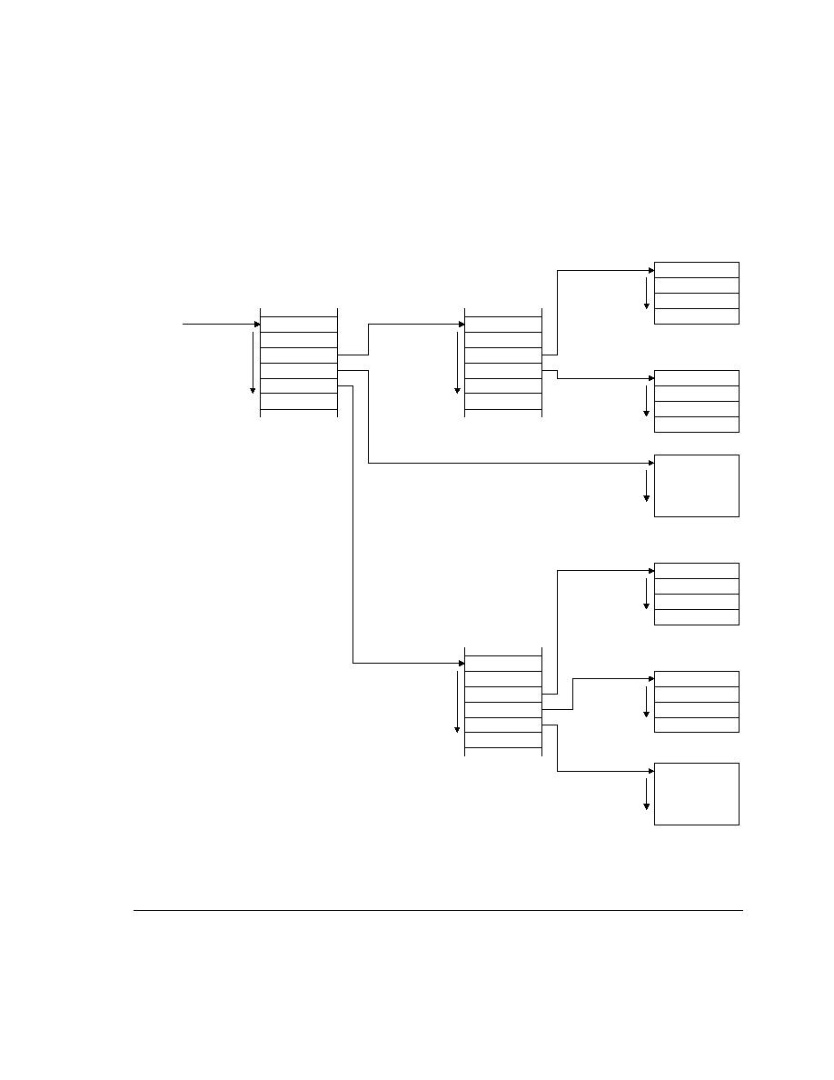
Memory Management Unit
ARM DDI 0244C
Copyright © 2003 ARM Limited. All rights reserved.
10-9
Figure 10-1 Address translation
Coarse page
table base
address from
L1D[31:10]
Large page base
address from
L2D[31:16]
Small page base
address from
L2D[31:12]
Section base address
from L1D[31:20]
1MB section
Indexed by
MVA[19:0]
4KB small page
1KB subpage
1KB subpage
1KB subpage
1KB subpage
Indexed by
MVA[11:0]
64KB large page
Indexed by
MVA[15:0]
16KB subpage
16KB subpage
16KB subpage
16KB subpage
31
0
Invalid 11
10
01
Large page base
address from
L2D[31:16]
Small page base
address from
L2D[31:12]
Tiny page base
address from
L2D[31:10]
Fine page table
base address from
L1D[31:12]
31
0
Invalid 00
11
10
01
1KB subpage
1KB subpage
1KB subpage
1KB subpage
4KB small page
Indexed by
MVA[11:0]
1KB tiny page
Indexed by
MVA[9:0]
16KB subpage
16KB subpage
16KB subpage
16KB subpage
64KB large page
Indexed by
MVA[15:0]
Level 2
7
0
7
0
7
0
7
0
7
0
7
0
1K 4-word
entries indexed
by MVA[19:10]
256 4-word
entries indexed
by MVA[19:12]
Invalid 00
Translation
table base
Level 1
31
0
01
10
11
4K 4-word
entries indexed
by MVA[31:20]
Invalid 00
16KB of level 1
page table
descriptors
1KB of level 2
coarse page table
descriptors
4KB of level 2
fine page table
descriptors
Pages and sections

Memory Management Unit
10-10
Copyright © 2003 ARM Limited. All rights reserved.
ARM DDI 0244C
10.3.3
Level 1 descriptor address
Figure 10-2 shows how the MMU creates the level 1 descriptor address from the CP15
c2 Translation Table Base Register and the MVA.
Figure 10-2 Translating a level 1 descriptor address
10.3.4
Level 1 descriptor
The level 1 descriptor indicates whether the access is:
∑
a translation fault
∑
an access to a level 2 coarse page table
∑
an access to a 1MB section of external memory
∑
an access to a level 2 fine page table.
Bits [1:0] of the level 1 descriptor determine the type of access. Figure 10-3 on
page 10-11 shows the level 1 descriptor format for each access type.
14
31
Translation table base
Not used
Level 1 table index
20
31
MVA
13
14
Level 1 table index
0
1
2
0
0
Translation table base
31
Level 1
descriptor
address
19
0
SBZ
0
CP15 c2
Translation Table Base Register
4
3 2
SBZ
L2B
L2C
13
5
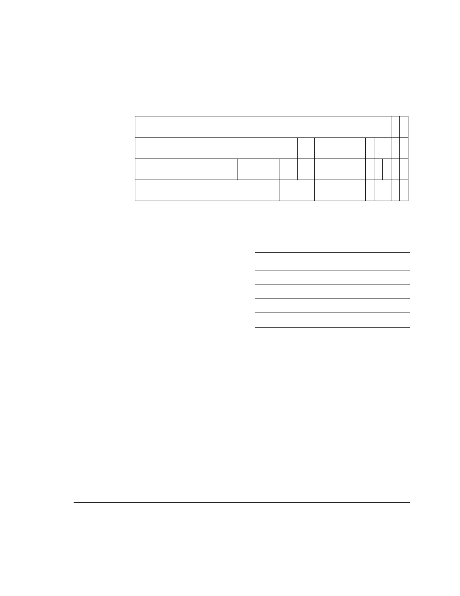
Memory Management Unit
ARM DDI 0244C
Copyright © 2003 ARM Limited. All rights reserved.
10-11
Figure 10-3 Level 1 descriptor formats
Bits [1:0] of the level 1 descriptor indicate the access type as Table 10-2 shows.
Level 1 translation fault
When bits [1:0] of the level 1 descriptor are b00, the MMU generates a translation fault.
This causes either a Prefetch Abort or Data Abort in the integer unit.
Level 1 coarse page table address
When bits [1:0] of the level 1 descriptor are b01, the MMU fetches a level 2 descriptor
from the coarse page table. Figure 10-6 on page 10-14 shows how the MMU generates
a coarse page table address.
Level 1 section base address
When bits [1:0] of the level 1 descriptor are b10, the MMU accesses a 1MB memory
section. Figure 10-4 on page 10-12 shows the translation process for a 1MB section.
31
20 19
12 11 10
9
8
5 4
1 0
0
0
1
0
1 SBZ
Domain selector
SBZ
Level 2 coarse page table base address
0
1
1 C B
AP
Section base address
SBZ
1
1
1
Level 2 fine page table base address
3 2
SBZ
Domain selector
Domain selector
SBZ
SBZ
Ignore
Translation fault
Coarse page table
1MB section
Fine page table
Table 10-2 Access type encoding in a level 1 descriptor
Bits [1:0]
Access type
b00
Translation fault
b01
Coarse page table base address
b10
Section base address
b11
Fine page table base address

Memory Management Unit
10-12
Copyright © 2003 ARM Limited. All rights reserved.
ARM DDI 0244C
Figure 10-4 Translating a section base address
Following translation of the level 1 descriptor for a section, the MMU checks the access
permissions for the section. If the access is permitted, the MMU uses the physical
address to transfer the requested data from external memory to the integer unit. MMU
memory access control on page 10-26 describes permission checking.
Level 1 fine page table base address
When bits [1:0] of the level 1 descriptor are b11, the MMU generates fetches a level 2
descriptor from the fine page table. Figure 10-9 on page 10-19 shows how the MMU
generates the fine page table address.
10 9
14
31
Translation table base
13
14
Level 1 table index
0
1
2
0
0
Translation table base
31
Level 1
descriptor
address
Section index
19
0
Level 1 table index
20
31
MVA
Domain
selector
19
0
Section base address
20
31
Level 1
descriptor
1211
AP
S
B
Z
8
5 4 3 2 1
0
1
C B
1
Level 1 fetch
Section index
19
0
Section base address
20
31
PA
SBZ
SBZ
0
CP15 c2
Translation Table Base Register
4
3 2
SBZ
L2B
L2C
13
5

Memory Management Unit
ARM DDI 0244C
Copyright © 2003 ARM Limited. All rights reserved.
10-13
10.3.5
Level 2 descriptor
If the level 1 descriptor points to a page table, the MMU determines the page table type,
coarse or fine, and fetches a level 2 descriptor from the page table. The level 2 descriptor
indicates whether the access is:
∑
a translation fault
∑
an access from a coarse page table to a 64KB large page
∑
an access from a coarse page table to a 4KB small page
∑
an access from a fine page table to a 64KB large page
∑
an access from a fine page table to a 4KB small page
∑
an access from a fine page table to a 1KB tiny page.
Figure 10-5 shows the level 2 descriptor format for each access type.
Figure 10-5 Level 2 descriptor formats
Bits [1:0] of the level 2 descriptor indicate the page type.
A large page can be divided into four 16KB subpages with different access permissions
defined by the AP fields. Bits [15:14] of the MVA page index select the subpages of a
large page.
A small page can be divided into four 1KB subpages with different access permissions.
Bits [11:10] of the MVA page index select the subpages of a small page.
Level 2 coarse page table descriptor
When the level 1 descriptor bits [1:0] indicate a descriptor fetch from a coarse page
table, the MMU requests the address of the level 2 coarse page table from external
memory. Figure 10-6 on page 10-14 shows how the coarse page table address is
generated.
0
1
0
B
AP3
Large page base address
0
1
C B
Small page base address
1
1
AP
Tiny page base address
SBZ
Ignore
Translation fault
64KB large page
4KB small page
1KB tiny page
0
31
16 15
12 11 10 9 8 7 6 5 4 3 2 1 0
SBZ
AP2 AP1 AP0 C
AP3 AP2 AP1 AP0
C B
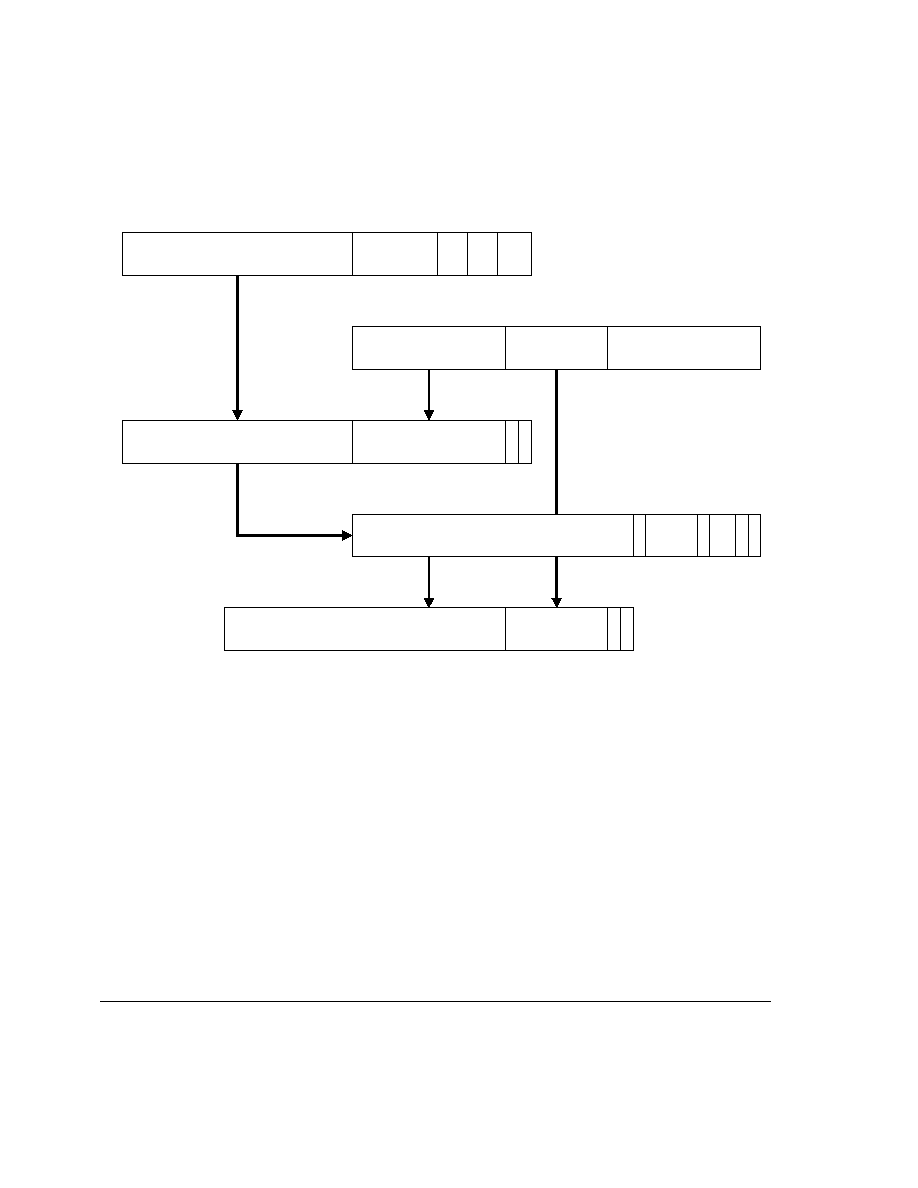
Memory Management Unit
10-14
Copyright © 2003 ARM Limited. All rights reserved.
ARM DDI 0244C
Figure 10-6 Translating a coarse page table address
Following translation of the level 1 descriptor for a section, the the MMU checks the
access permissions for the section. If the access is permitted, the MMU uses the
physical address to transfer the requested data from external memory to the integer unit.
Level 1
descriptor
address
MVA
10 9
14
31
Translation table base
13
14
Level 1 table index
0
1
2
0
0
Translation table base
31
Level 2
table index
19
0
Level 1 table index
20
31
Domain
selector
0
Page table base address
31
Level 1
descriptor
Not used
S
B
Z
8
5 4
1
1
0
1
Level 1 fetch
S
B
Z
3 2
12 11
0
Page table base address
31
Level 2
table index
0
1
2
9
10
Level 2
descriptor
address
SBZ
0
CP15 c2
Translation Table Base Register
4
3 2
SBZ
L2B
L2C
13
5
0

Memory Management Unit
ARM DDI 0244C
Copyright © 2003 ARM Limited. All rights reserved.
10-15
When the coarse page table address is generated, a request is made to external memory
for the level 2 coarse page table descriptor. Bits [1:0] of the level 2 coarse page table
descriptor indicate the access type as shown in Table 10-3.
Level 2 coarse translation fault
If bits [1:0] of the level 2 coarse page table descriptor are b00 or b11, then a translation
fault is generated. This generates an abort to the integer unit, either a Prefetch Abort for
the instruction side or a Data Abort for the data side.
Level 2 coarse large page base address
If bits [1:0] of the level 2 coarse page table descriptor are b01, then a descriptor fetch
from a coarse large page table is required. Figure 10-7 on page 10-16 shows the
translation process for a 64KB large page or a 16KB subpage of a large page.
Table 10-3 Access type encoding in a coarse page table descriptor
Bits[1:0]
Access type
b00
Translation fault
b01
64KB large page base address
b10
4KB small page base address
b11
Translation fault

Memory Management Unit
10-16
Copyright © 2003 ARM Limited. All rights reserved.
ARM DDI 0244C
Figure 10-7 Translating a large page or subpage address from a coarse page table
The 64KB large page is generated by setting all of the AP bit pairs to the same values,
AP3 = AP2 = AP1 = AP0. If any one of the pairs is different, then the 64KB large page
is converted into four 16KB subpages.
10
31
Level 1
descriptor
address
0
1
2
MVA
Level 2
table index
Level 1 table index
20
31
Level 1
descriptor
Page index
Level 1
fetch
15
Level 2
descriptor
address
16
0
Page table base address
31
Level 2
table index
0 0
1
10
0
31
1
2
9
10
Level 2
descriptor
13
14
31
Level 1 table index
0
0
Translation table base
14
31
Translation table base
Level 2
fetch
1211
8 7 6 5 4 3
Page base address
SBZ
A
P
3
A
P
2
A
P
1
A
P
0
C B 0
11
19
12
0
PA
Page base address
Page index
9
0
8
5 4
1
3 2
Domain
selector
Page table base address
S
B
Z
1
0
1
S
B
Z
1
16 15
2
9
31
16
0
15
SBZ
0
CP15 c2
Translation Table Base Register
4
3 2
SBZ
L2B
L2C
13
5

Memory Management Unit
ARM DDI 0244C
Copyright © 2003 ARM Limited. All rights reserved.
10-17
Note
The level 2 coarse page table index uses MVA[19:12], and the large page index uses
MVA[15:0]. The overlapping four bits, MVA[15:12], require groups of 16 consecutive
entries in the level 2 page tables to contain duplicate entries.
Level 2 coarse small page base address
If bits [1:0] of the level 2 coarse page table descriptor are b10, then a descriptor fetch
from a coarse small page table is required. Figure 10-8 on page 10-18 shows the
translation process for a 4KB small page or a 1KB subpage of a small page.

Memory Management Unit
10-18
Copyright © 2003 ARM Limited. All rights reserved.
ARM DDI 0244C
Figure 10-8 Translating a small page or subpage address from a coarse page table
The 4KB small page is generated by setting all of the AP bit pairs to the same values,
AP3 = AP2 = AP1 = AP0. If any one of the pairs are different, then the 4KB small page
is converted into four 1KB small page subpages.
Level 1
descriptor
address
0
1
2
MVA
Level 2
table index
Level 1 table index
20
31
Level 1
descriptor
Page index
Level 1
fetch
Level 2
descriptor
address
0
Page table base address
31
Level 2
table index
0
0
1
2
9
10
0
1
2
9
10
Level 2
descriptor
13
14
31
Level 1 table index
0
0
Translation table base
14
31
Translation table base
Level 2
fetch
11
8 7 6 5 4 3
Page base address
0
A
P
3
A
P
2
A
P
1
A
P
0
C B 1
0
11
19
12
10 9
0
31
8
5 4
1
3 2
Domain
selector
Page table base address
S
B
Z
1
0
1
S
B
Z
PA
0
Page base address
31
Page index
12 11
31
12
SBZ
0
CP15 c2
Translation Table Base Register
4
3 2
SBZ
L2B
L2C
13
5

Memory Management Unit
ARM DDI 0244C
Copyright © 2003 ARM Limited. All rights reserved.
10-19
Level 2 fine page table descriptor
When the level 1 descriptor bits [1:0] indicate that a descriptor fetch from a fine page
table is required, the MMU requests the level 2 fine page table address from external
memory. Figure 10-9 shows how the address is generated.
Figure 10-9 Translating a fine page table address
11
2
Level 1
descriptor
address
0
1
2
MVA
9
Level 2
table index
0
Level 1 table index
20
31
0
Level 1
descriptor
Not used
8
5 4
1
Level 1 fetch
3 2
10
19
Level 2
descriptor
address
13
14
31
Level 1 table index
0
0
Translation table base
14
31
Translation table base
9
11
0
Fine page table base address
Level 2
table index
0
0
1
12
31
Domain
selector
Fine page table base address
1
1
S
B
Z
SBZ
1
31
12
SBZ
0
CP15 c2
Translation Table Base Register
4
3 2
SBZ
L2B
L2C
13
5

Memory Management Unit
10-20
Copyright © 2003 ARM Limited. All rights reserved.
ARM DDI 0244C
Following translation of the level 1 descriptor for the base address of a fine page table
address, the MMU requests checks the access permissions for the section. If the access
is permitted, the MMU uses the physical address to transfer the requested data from
external memory to the integer unit. When the fine page table address is generated, a
request is made to external memory for the level 2 fine page table descriptor. Bits [1:0]
of the level 2 fine page table descriptor indicate the access type as shown in Table 10-4.
Level 2 fine translation fault
If bits [1:0] of the level 2 fine page table descriptor are b00, then a translation fault is
generated. This causes either a Prefetch Abort or a Data Abort in the integer unit. A
Prefetch Abort occurs on the instruction side, while a Data Abort occurs on the data
side.
Level 2 fine large page base address
If bits [1:0] of the level 2 fine page table descriptor are b01, then a descriptor fetch from
a fine large page table is required. Figure 10-10 on page 10-21 shows the translation
process for a 64KB large page or a 16KB subpage of a large page.
Table 10-4 Access type encoding in a fine page table descriptor
Bits [1:0]
Access type
b00
Translation fault
b01
Large page table base address
b10
Small page base address
b11
Tiny page table base address

Memory Management Unit
ARM DDI 0244C
Copyright © 2003 ARM Limited. All rights reserved.
10-21
Figure 10-10 Translating a large page or subpage address from a fine page table
The 64KB large page is generated by setting all of the AP bit pairs to the same values,
AP3 = AP2 = AP1 = AP0. If any pair is different from the others, then the 64KB large
page is converted into four 16KB subpages.
PA
Level 1
descriptor
address
0
1
2
MVA
Level 2
table index
0
Level 1 table index
20
31
Level 1
descriptor
Page index
Level 1
fetch
19
Level 2
descriptor
address
13
14
31
Level 1 table index
0
0
Translation table base
14
31
Translation table base
16 15
10 9
9
0
8
5 4
1
3 2
Domain
selector
Page table base address
1
1
S
B
Z
11
SBZ
1
31
12
Level 2
fetch
0
Page table base address
Level 2
table index
0
0
1
2
12 11
31
0
1
2
Page table base address
Page index
31
16
12
0
15
1110 9 8 7
4 3
31
Level 2
descriptor
6 5
A
P
2
A
P
1
A
P
0
1
0
C B
A
P
3
15
16
SBZ
Page table base address
SBZ
0
CP15 c2
Translation Table Base Register
4
3 2
SBZ
L2B
L2C
13
5

Memory Management Unit
10-22
Copyright © 2003 ARM Limited. All rights reserved.
ARM DDI 0244C
Note
The level 2 fine page table index uses MVA[19:10], and the large page index uses
MVA[15:0]. The overlapping six bits, MVA[15:10], require groups of 64 consecutive
entries in the level 2 page tables to contain duplicate entries.
Level 2 fine small page base address
If bits [1:0] of the level 2 fine page table descriptor are b10, then a descriptor fetch from
a fine small page table is required. Figure 10-11 on page 10-23 shows the translation
process for a 4KB small page or a 1KB subpage of a small page.
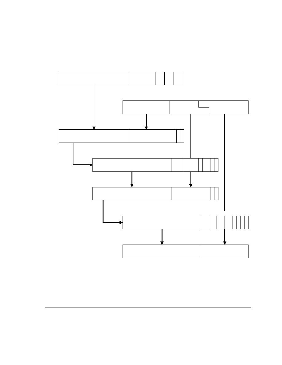
Memory Management Unit
ARM DDI 0244C
Copyright © 2003 ARM Limited. All rights reserved.
10-23
Figure 10-11 Translating a small page or subpage address from a fine page table
The 4KB small page is generated by setting all of the AP bit pairs to the same values,
AP3 = AP2 = AP1 = AP0. If any one of the pairs are different, then the 4KB small page
is converted into four 1KB small page subpages.
PA
Level 1
descriptor
address
0
1
2
MVA
Level 2
table index
0
Level 1 table index
20
31
Level 1
descriptor
Page index
Level 1
fetch
19
Level 2
descriptor
address
13
14
31
Level 1 table index
0
0
Translation table base
14
31
Translation table base
12 11 10 9
9
0
8
5 4
1
3 2
Domain
selector
Page table base address
1
1
S
B
Z
11
SBZ
1
31
12
Level 2
fetch
0
Page table base address
Level 2
table index
0
0
1
2
12 11
31
0
1
2
Page table base address
Page index
31
12
0
11
1110 9 8 7
4 3
Level 2
descriptor
12
31
6 5
Page table base address
A
P
3
A
P
2
A
P
1
A
P
0
0
1
C B
SBZ
0
CP15 c2
Translation Table Base Register
4
3 2
SBZ
L2B
L2C
13
5

Memory Management Unit
10-24
Copyright © 2003 ARM Limited. All rights reserved.
ARM DDI 0244C
Note
The level 2 fine page table index uses MVA[19:10], and the small page index uses
MVA[11:0]. The overlapping two bits, MVA[11:10], require groups of four
consecutive entries in the level 2 page tables to contain duplicate entries.
Level 2 fine tiny page base address
If bits [1:0] of the level 2 fine page table descriptor are b11, then a descriptor fetch from
a fine tiny page table is required. Figure 10-12 on page 10-25 shows the translation
process for a 1KB tiny page.

Memory Management Unit
ARM DDI 0244C
Copyright © 2003 ARM Limited. All rights reserved.
10-25
Figure 10-12 Translating a tiny page address
SBZ
0
CP15 c2
Translation Table Base Register
4
3 2
SBZ
L2B
L2C
13
5
PA
Level 1
descriptor
address
0
1
2
MVA
Level 2 table index
0
Level 1 table index
20
31
Level 1
descriptor
Page index
Level 1
fetch
19
Level 2
descriptor
address
13
14
31
Level 1 table index
0
0
Translation table base
14
31
Translation table base
10 9
9
0
8
5 4
1
3 2
Domain
selector
Page table base address
1
1
S
B
Z
11
SBZ
1
31
12
Level 2
fetch
0
Page table base address
Level 2
table index
0
0
1
2
12 11
31
0
1
2
Page table base address
Page index
31
0
9
4 3
Level 2
descriptor
10 9
6 5
SBZ
AP
1
1
C B
Page table base address
10
31

Memory Management Unit
10-26
Copyright © 2003 ARM Limited. All rights reserved.
ARM DDI 0244C
10.4
MMU memory access control
Memory domains support multiuser operating systems. All regions of memory have an
associated domain. Domains are the primary memory access control mechanism and
define the conditions in which an access can proceed. Each domain determines whether:
∑
access is qualified to proceed as shown in Table 10-6 on page 10-27
∑
access is unconditionally enabled to proceed
∑
access is unconditionally aborted.
In the latter two cases, the access permission attributes are ignored. There are 16
domains, D15-D0, that are configured in the CP15 c3 Domain Access Control Register.
The domain definition provides access for two types of users, manager and client. The
two-bit D15-D0 fields in the Domain Access Control Register control access to both the
instruction and data domains. Table 10-5 shows the encoding for of the domain access
control fields.
A manager access is checked only against the access permissions for the domain. A
client access is checked against the domain access permissions and against the system
protection bit, S, and the ROM protection bit, R, in the CP15 c1 Control Register.
Table 10-6 on page 10-27 shows the effect of the S and R bits.
Table 10-5 Domain access encoding
D15-D0
User
Notes
b00
No access
Access generates a domain fault.
b01
Client
Access permissions are checked.
b10
Reserved
Behaves as a no access domain.
b11
Manager
Access permissions are not checked.

Memory Management Unit
ARM DDI 0244C
Copyright © 2003 ARM Limited. All rights reserved.
10-27
Table 10-6 MMU memory access control
AP
CP15
S bit
CP15
R bit
Supervisor
User
Meaning
b00
0
0
-
-
Permission fault
b00
1
0
Read
-
Read-only in Supervisor mode
b00
0
1
Read
Read
Permission fault on writes
b00
1
1
Reserved
Reserved
Permission fault on reads or writes
b01
-
-
Read/write
-
Permission fault on reads or writes in User mode
b10
-
-
Read/write
Read
Read-only in User mode
b11
-
-
Read/write
Read/write
All accesses permissible

Memory Management Unit
10-28
Copyright © 2003 ARM Limited. All rights reserved.
ARM DDI 0244C
10.5
MMU cachable and bufferable information
The Cachable (C) and Bufferable (B) bits in the level 1 and level 2 descriptors control
the operation of memory accesses to external memory. Table 10-7 indicates how the
MMU and cache interpret the C and B bits.
Table 10-7 C and B bit access control
C
B
Memory access
0
0
Noncachable, nonbufferable
0
1
Noncachable, bufferable
1
0
Write-through cachable, bufferable
1
1
Write-back cachable, bufferable

Memory Management Unit
ARM DDI 0244C
Copyright © 2003 ARM Limited. All rights reserved.
10-29
10.6
MMU and pending write buffer
During any descriptor fetch, the MMU has access to external memory. The integer unit
is stalled during any descriptor fetch.
Before an MMU descriptor fetch, the pending write buffer has to be drained to preserve
memory coherency. If the pending write buffer contains any page table entries that have
been modified, those entries are forced to external memory as a result of the descriptor
fetch.
When the MMU contains valid TLB entries that are being modified, these TLB entries
must be invalidated before the new section or page is accessed. This also applies to any
data that resides in the ICache or DCache. The ICache lines must be invalidated, and
the DCache line or lines must be cleaned and invalidated.

Memory Management Unit
10-30
Copyright © 2003 ARM Limited. All rights reserved.
ARM DDI 0244C
10.7
Fault checking sequence
During the processing of a section or page, the MMU checks for faults. This section
describes the following conditions:
∑
External abort on translation
∑
Address alignment fault
∑
Translation fault
∑
Domain fault on page 10-32
∑
Permission fault on page 10-32.
Figure 10-13 on page 10-31 shows the fault checking sequence.
10.7.1
External abort on translation
If the BIU returns an error due to a level 1 or level 2 descriptor fetch, the MMU signals
an abort and stops processing the hardware page table walk. No entry is written to the
TLB.
10.7.2
Address alignment fault
An address alignment fault occurs whenever the integer unit indicates a particular data
memory access size and the address does not comply with that size. If MAS[1:0] = b10
indicating a 32-bit access, and the MVA bits [1:0]
b00, then an address alignment
fault occurs. If MAS[1:0] = b01 indicating a 16-bit access, and the MVA bit 0
0, then
an address alignment fault occurs. No check is performed when MAS[1:0] = b00.
Alignment checks are performed with the MMU both on and off and only for data
memory accesses.
10.7.3
Translation fault
Two types of translation faults occur:
∑
section
∑
page.
A section translation fault results from an invalid level 1 descriptor. Bits [1:0] of the
descriptor are b00.
A page translation fault results from an invalid level 2 descriptor. Bits [1:0] of the
coarse page table descriptor are b00 or b11, or bits [1:0] of the fine page table descriptor
are b00.

Memory Management Unit
ARM DDI 0244C
Copyright © 2003 ARM Limited. All rights reserved.
10-31
Figure 10-13 Fault checking flowchart
Level 1 descriptor fetch
Start
Modified virtual address
N
Y
Alignment
fault
Checking
alignment?
Address
aligned?
Section
Coarse
Level 2 descriptor fetch
Fine
Y
N
Section
translation
fault
Section
domain
fault
Section
or page?
Descriptor
fault?
Domain
fault?
Coarse
or fine?
External
abort?
Y
Y
N
N
Y
Y
N
N
Page
domain
fault
Page
translation
fault
Domain
fault?
Domain
fault?
Descriptor
fault?
Descriptor
fault?
Page
translation
fault
Page
domain
fault
External
abort?
External abort
on level 2
translation
External abort
on level 2
translation
Y
Y
N
N
External
abort?
External abort
on level 1
translation
Y
N
Y
N
Y
N
Page
Client
Physical address
Manager
Manager
Coarse
Fine
Client
N
N
N
Y
Y
Y
Page access
permission
fault
Page access
permission
fault
Domain
type?
Domain
type?
Section access
permission fault
Access
permission
fault?
Access
permission
fault?
Access
permission
fault?

Memory Management Unit
10-32
Copyright © 2003 ARM Limited. All rights reserved.
ARM DDI 0244C
10.7.4
Domain fault
Three types of domain faults occur:
∑
section
∑
coarse page
∑
fine page.
For each type, the level 1 descriptor indicates which domain to select in the CP15 c3
Domain Access Control Register. If bit 0 of the selected domain is zero, indicating
either No access or Reserved, then a domain fault occurs. A section domain fault occurs
when the level 1 descriptor is returned. Both the coarse and fine page domain faults are
checked whenever the level 2 descriptor is returned.
The MMU empties any unlocked TLB entry following a write to the CP15 c3 Domain
Access Control Register (DACR). To guarantee the behavior, all locked TLB entries
must not modify their DACR entry. If the DACR entry is modified, the TLB entry must
be unlocked and invalidated.
10.7.5
Permission fault
There are three types of access permission faults:
∑
section
∑
coarse page
∑
fine page.
Whenever the domain indicates that a client has accessed a region of memory, an access
permission check follows. If the access does not comply with the access permission
table, then a fault corresponding to the access type occurs. A section permission fault
check occurs when the level 1 descriptor is returned and is designated as a client. Both
the coarse and fine page permission faults are checked whenever the level 2 descriptor
is returned and is designated as a client.

Memory Management Unit
ARM DDI 0244C
Copyright © 2003 ARM Limited. All rights reserved.
10-33
10.8
Fault priority
Table 10-8 lists MMU faults in order of priority, from highest to lowest.
The values in the domain field are invalid when the fault occurs before the MMU reads
the domain field from a page table descriptor. Any abort masked by the priority
encoding can be regenerated by fixing the primary abort and restarting the instruction.
Table 10-8 MMU faults
Priority
Fault type
Status
[10], [3:0]
Domain
FAR
Highest
Imprecise external abort
1, b0110
Invalid
Valid
a
a. The CP15 c6 Fault Address Register reflects the address of the load or store to which the
imprecise abort is attached, not the address of the external abort.
Alignment fault
0, b0001
Invalid
Valid
TLB miss
0, b0000
Invalid
Valid
Level 1 translation precise external abort
0, b1100
Invalid
Valid
Level 1 section translation fault
0, b0101
Invalid
Valid
Level 2 translation precise external abort
0, b1110
Valid
Valid
Level 2 page translation fault
0, b0111
Valid
Valid
Section domain fault
0, b1001
Valid
Valid
Page domain fault
0, b1011
Valid
Valid
Section access permission fault
0, b1101
Valid
Valid
Page access permission fault
0, b1111
Valid
Valid
Nontranslation precise external abort
0, b000
Valid
Valid
Lowest
Debug breakpoint or watchpoint
0, b0010
Valid
Valid

Memory Management Unit
10-34
Copyright © 2003 ARM Limited. All rights reserved.
ARM DDI 0244C
10.9
MMU aborts and external aborts
The MMU generates aborts on MMU faults and also makes the properties of both
precise and imprecise external aborts visible.
10.9.1
MMU faults
When the MMU detects a fault during any memory access, it generates a Prefetch Abort
or a Data Abort, and the integer unit enters the Prefetch Abort handler or the Data Abort
handler. The MMU generates aborts on six types of MMU faults:
∑
alignment fault
∑
TLB miss when ADTM bit is set (see CP15 c15 Debug Override Register on
page 3-53)
∑
translation fault
∑
domain fault
∑
permission fault
∑
debug breakpoint or watchpoint.
An alignment fault can be caused only by a data access. The A bit in the CP15 c1
Control Register enables alignment fault checking. Alignment fault checking can be
enabled even when the MMU is disabled.
An MMU miss, translation fault, domain fault, or permission fault can be caused by a
data access or an instruction access.
10.9.2
External aborts
The MMU performs external abort fault checking to enable you to observe the
properties of both precise and imprecise external aborts. Precise aborts are always
enabled. The IMA bit in the CP15 c15 Debug Override Register statically enables
imprecise aborts. Imprecise aborts are enabled by default. See Chapter 16 External
Aborts for a full explanation of external abort behavior.
10.9.3
Fault address registers and fault status registers
The CP15 c5 Instruction Fault Status Register contains the type of MMU fault or
external abort that occurred. The CP15 c6 Instruction Fault Address Register contains
the MVA of the access that caused the MMU fault or external abort.
The CP15 c5 Data Fault Status Register contains the type of MMU fault or external
abort that occurred. The CP15 c6 Data Fault Status Register contains the MVA of the
access that caused the MMU fault or external abort.
See Table 10-8 on page 10-33 for fault codes and priorities.

Memory Management Unit
ARM DDI 0244C
Copyright © 2003 ARM Limited. All rights reserved.
10-35
10.10 Memory parity
The parity generator is an odd-parity circuit that produces parity bits on a per-byte basis.
If a byte has an even number of 1s, the parity generator appends another 1 to the byte
to produce a nine-bit code word that has an odd number of 1s. Parity generation is not
configurable.
Because the ARM1026EJ-S processor does not provide parity error detection, storing
and handling the parity bit information is the responsibility of the system designer. If
parity error detection is not required, the parity outputs can remain unconnected.
10.10.1 MMU parity interfaces
The MMU write interface is split into a 22-bit TLB tag write data interface and a 34-bit
TLB data write data interface. The TLB is two-way set-associative, resulting in 112 bits
total. Parity bit generation is provided for both the tag and data portions of the TLB data
write interface. Table 10-9 lists the TLB data bytes and their parity bits.
Table 10-9 MMU TLB parity interfaces
Data byte
Parity bit
I/O
TLB tag write parity interface
MMUxWD[111:106]
a
MMUTAGPAR[5]
O
MMUxWD[105:98]
MMUTAGPAR[4]
O
MMUxWD[97:90]
MMUTAGPAR[3]
O
MMUxWD[55:50]
a
MMUTAGPAR[2]
O
MMUxWD[49:42]
MMUTAGPAR[1]
O
MMUxWD[41:34]
MMUTAGPAR[0]
O
TLB data write parity interface
MMUxWD[89:88]
b
MMUDATAPAR[9]
O
MMUxWD[87:80]
MMUDATAPAR[8]
O
MMUxWD[79:72]
MMUDATAPAR[7]
O
MMUxWD[71:64]
MMUDATAPAR[6]
O
MMUxWD[63:56]
MMUDATAPAR[5]
O
MMUxWD[33:32]
b
MMUDATAPAR[4]
O

Memory Management Unit
10-36
Copyright © 2003 ARM Limited. All rights reserved.
ARM DDI 0244C
MMUxWD[31:24]
MMUDATAPAR[3]
O
MMUxWD[23:16]
MMUDATAPAR[2]
O
MMUxWD[15:8]
MMUDATAPAR[1]
O
MMUxWD[7:0]
MMUDATAPAR[0]
O
a. Because the data in this field has only six bits, the
resulting code word has seven bits.
b. Because the data in this field has only two bits, the
resulting code word has three bits.
Table 10-9 MMU TLB parity interfaces (continued)
Data byte
Parity bit
I/O

ARM DDI 0244C
Copyright © 2003 ARM Limited. All rights reserved.
11-1
Chapter 11
Memory Protection Unit
This chapter describes the Memory Protection Unit (MPU). It contains the following
sections:
∑
About the MPU on page 11-2
∑
MPU software-accessible registers on page 11-3
∑
Configuring the MPU on page 11-5
∑
Overlapping protection regions on page 11-8
∑
Fault priority on page 11-9
∑
MPU aborts and external aborts on page 11-10.
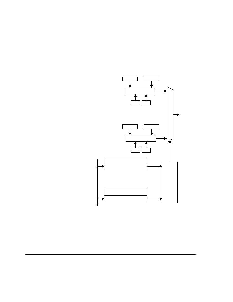
Memory Protection Unit
11-2
Copyright © 2003 ARM Limited. All rights reserved.
ARM DDI 0244C
11.1
About the MPU
As Figure 11-1 shows, you can use the MPU to partition external memory into eight
protection regions with different sizes and attributes.
Figure 11-1 MPU block diagram
.
.
.
Protection Region Register 7
Address
bus
Region 0 comparator
Hit 7
Hit 0
Priority
encoder
Region 7 comparator
Protection Region Register 0
.
.
.
or AP0[1:0]
AP0[3:0]
Protection region 7
or AP7[1:0]
AP7[3:0]
Protection region 0
C7
B7
C0
B0
Attributes
for current
transfer

Memory Protection Unit
ARM DDI 0244C
Copyright © 2003 ARM Limited. All rights reserved.
11-3
11.2
MPU software-accessible registers
The CP15 registers listed in Table 11-1 on page 11-4 control MPU operation.
All the registers in Table 11-1 on page 11-4 except CP15 c8 contain state and can be
read using MRC instructions and written to using MCR instructions.
Chapter 3 Programmer's Model describes the CP15 registers in more detail.

Memory Protection Unit
11-4
Copyright © 2003 ARM Limited. All rights reserved.
ARM DDI 0244C
Table 11-1 CP15 MPU registers
Register
Bit
Description
CP15 c1 Control
Register
0
1
MPU enable bit:
1 = MPU enabled
0 = MPU disabled.
Address alignment fault checking enable bit:
1 = fault checking of address alignment enabled
0 = fault checking of address alignment disabled.
CP15 c2 DCache and
ICache Configuration
Registers
[7:0]
Cachable bits:
1 = DCache or ICache protection region cachable
0 = DCache or ICache protection region noncachable.
CP15 c3 Write Buffer
Control Register
[7:0]
Protection region bufferable bits:
1 = protection region bufferable
0 = protection region nonbufferable.
CP15 c5 Fault Status
Registers
[31:11]
[7:4]
10, [3:0]
Should Be Zero.
Protection region (0-7) in which fault occurred:
b0000 = protection region 0
b0001 = protection region 1
. . .
b0111 = protection region 7.
Fault type that caused Data Abort or Prefetch Abort. See Table 11-2 on page 11-9.
CP15 c5 Extended
Access Permission
Registers
[31:28]
[27:24]
. . .
[3:0]
Extended format access permission field for protection region 7.
Extended format access permission field for protection region 6.
. . .
Extended format access permission field for protection region 0.
CP15 c5 Standard
Access Permission
Registers
[15:14]
[13:12]
. . .
[1:0]
Standard format access permission field for protection region 7.
Standard format access permission field for protection region 6.
. . .
Standard format access permission field for protection region 0.
CP15 c6 Fault Address
Registers
[31: 0]
MVA of access that caused Data Abort or Prefetch Abort. ARM10EJ-S register
R14_abt holds VA that caused Prefetch Abort.
CP15 c6 Protection
Region Registers 0-7
[31:12]
[11:6]
[5:1]
0
Base address of protection region.
Should Be Zero.
Size of protection region.
Protection region enable bit.

Memory Protection Unit
ARM DDI 0244C
Copyright © 2003 ARM Limited. All rights reserved.
11-5
11.3
Configuring the MPU
This section describes how to select the MPU and initialize the protection regions.
11.3.1
Selecting the MPU
The MMUnMPU pin is a static input that configures the ARM1026EJ-S processor to
use either the MPU or the Memory Management Unit (MMU). To use the MPU, tie the
MMUnMPU input LOW.
11.3.2
Initializing the protection regions
The ARM architecture uses constants known as inline literals to perform address
calculations. These constants are automatically generated by the assembler and
compiler and are stored inline with the instruction code. To ensure correct operation,
the code that initializes and enables the MPU must lie in a valid protection region that
allows both data and instruction accesses.
To initialize the MPU, use CP15 registers c6, c5, c3, c2, and c1 to:
∑
program the base address, size, and enable bit of each protection region
∑
program the access permission of each protection region
∑
enable or disable bufferability of each protection region
∑
enable or disable cachability of each protection region
∑
enable the MPU.
Protection region base address, size, and enable
For each protection region, CP15 c6 has a Protection Region Register (PRR) that:
∑
defines the base address of the protection region
∑
defines the size of the protection region
∑
enables the protection region.
The base address is the first address of the memory region. You must align the base
address on a region-sized boundary. For example, an 8KB region must have a base
address that is a multiple of 8K.
Note
Incorrrectly aligned regions cause Unpredictable behavior.
A five-bit field in each PRR selects a region size from 4KB to 4GB.
Bit 0 of each PRR enables the protection region.

Memory Protection Unit
11-6
Copyright © 2003 ARM Limited. All rights reserved.
ARM DDI 0244C
CP15 c5 Protection Region Registers on page 3-34 has the instructions for using the
Protection Region Registers.
Access permission
CP15 c5 has four access permission registers:
∑
CP15 c5 Data and Instruction Extended Access Permission Registers on
page 3-29
∑
CP15 c5 Data and Instruction Standard Access Permission Registers on
page 3-31.
The extended access permission registers have four-bit fields to control data-access
permission and instruction-access permission for each protection region. The standard
access permission registers have two-bit access permission fields.
A memory abort occurs when an access fails its protection check. For example, a User
mode attempt to access a privileged mode access only protection region causes a
memory abort. The processor enters the abort exception mode, branching to the Data
Abort or Prefetch Abort vector.
Write buffer configuration
The CP15 c3 Write Buffer Control Register has a bufferable bit for each protection
region. The Write Buffer Control Register affects only data accesses.
CP15 c3 Write Buffer Control Register on page 3-25 has the instructions for using the
Write Buffer Control Register.
Cache configuration
The CP15 c2 DCache Configuration Register contains a cachable bit for data accesses
to each protection region. The CP15 c2 ICache Configuration Register contains a
cachable bit for instruction accesses to each protection region.
CP15 c2 DCache and ICache Configuration Registers on page 3-21 has the instructions
for using the DCache and ICache Configuration Registers.

Memory Protection Unit
ARM DDI 0244C
Copyright © 2003 ARM Limited. All rights reserved.
11-7
Enabling the MPU
The M bit in the CP15 c1 Control Register enables the MPU.
Note
∑
Do not enable the MPU without initializing at least one protection region.
∑
When the MPU is disabled and the ICache is enabled, all instruction fetches are
cachable. If the ICache is disabled, all instruction fetches are noncachable.
∑
When the MPU is disabled, all data accesses are noncachable and nonbufferable
whether the DCache is enabled or disabled.
You can use the CP15 c15 Debug Override Register and the CP15 c15 Memory
Region Remap Register to change this default behavior.
CP15 c1 Control Register on page 3-14 has the instructions for using the Control
Register.
Memory Protection Unit
11-8
Copyright © 2003 ARM Limited. All rights reserved.
ARM DDI 0244C
11.4
Overlapping protection regions
You can program the MPU with two or more overlapping protection regions. When the
processor accesses overlapping protection regions, the attributes of the
highest-numbered protection region control the access. Attributes for protection region
7 have the highest priority, and attributes for protection region 0 have the lowest
priority. For example:
Region 1
16KB deep, starting from address
0x0000
. No User mode access.
Region 2
4KB deep, starting from address
0x3000
. User mode access
permissions are read-only.
A User mode read to address
0x3010
falls into both protection regions 1 and 2, as shown
in Figure 11-2. The conflict between the permissions of the overlapping protection
regions causes the attributes of protection region 2 take effect. Although a User mode
read to protection region 1 can cause a Data Abort, the overlapping protection region 2
permits the read to
0x3010
.
Figure 11-2 Overlapping protection regions
You can overlap protection regions to create a background region. For example, you
might have a number of physical memory areas sparsely distributed across the 4GB
address space. If a programming error occurs, the processor might issue an address that
does not fall into any defined protection region, causing the MPU to abort the access.
You can prevent this kind of abort by programming region 0 to be a 4GB background
region. In this way, if the address does not fall into any of the other seven regions, the
access is controlled by the attributes you specify for region 0.
0x4000
0x3010
0x3000
0x0000
Region 1, User: no access
Region 2, User: read-only
Read-only User permission of region 2 overrides
no-User-access permission of region 1

Memory Protection Unit
ARM DDI 0244C
Copyright © 2003 ARM Limited. All rights reserved.
11-9
11.5
Fault priority
Table 11-2 lists MPU faults in order of priority, from highest to lowest.
The values in the domain field are invalid when the fault occurs before the MPU reads
the domain field from a page table descriptor. Any abort masked by the priority
encoding can be regenerated by fixing the primary abort and restarting the instruction.
Table 11-2 MPU faults
Priority
Fault type
Status
[10], [3:0]
Domain
FAR
Highest
Imprecise external abort
1, b0110
Invalid
Valid
a
a. The CP15 c6 Fault Address Register reflects the address of the load or store to which
the imprecise abort is attached, not the address of the external abort.
Alignment fault
0, b0001
Invalid
Valid
MPU miss
0, b0000
Invalid
Valid
Access permission fault
0, b1101
Valid
Valid
Nontranslation precise external abort
0, b1000
Valid
Valid
Lowest
Debug breakpoint or watchpoint
0, b0010
Valid
Valid

Memory Protection Unit
11-10
Copyright © 2003 ARM Limited. All rights reserved.
ARM DDI 0244C
11.6
MPU aborts and external aborts
The MPU generates aborts on MPU faults and also makes the properties of both precise
and imprecise external aborts visible.
11.6.1
MPU faults
When the MPU detects a fault during any memory access, it generates a Prefetch Abort
or a Data Abort, and the integer unit enters the Prefetch Abort handler or the Data Abort
handler. The MPU generates aborts on four types of MPU faults:
∑
alignment fault
∑
MPU miss
∑
permission fault
∑
debug breakpoint or watchpoint.
An alignment fault can be caused only by a data access. The A bit in the CP15 c1
Control Register enables alignment fault checking. Alignment fault checking can be
enabled even when the MPU is disabled.
An MPU miss or permission fault can be caused by a data access or an instruction
access.
11.6.2
External aborts
The MPU performs external abort fault checking to enable you to observe the properties
of both precise and imprecise external aborts. Precise aborts are always enabled. The
IMA bit in the CP15 c15 Debug Override Register enables imprecise aborts. Imprecise
aborts are enabled by default. See Chapter 16 External Aborts for a full explanation of
external abort behavior.
11.6.3
Fault address registers and fault status registers
The CP15 c5 Instruction Fault Status Register contains the type of MPU fault or
external abort that occurred.The CP15 c6 Instruction Fault Address Register contains
the MVA of the access that caused the MPU fault or external abort.
The CP15 c5 Data Fault Status Register contains the type of MPU fault or external abort
that occurred. The CP15 c6 Data Fault Address Register contains the MVA of the
access that caused the MPU fault or external abort.
See Table 11-2 on page 11-9 for fault codes and priorities.

ARM DDI 0244C
Copyright © 2003 ARM Limited. All rights reserved.
12-1
Chapter 12
Caches
This chapter describes the ICache and DCache. It contains the following sections:
∑
About the caches on page 12-2
∑
Enabling the caches on page 12-3
∑
Cache and TCM access priorities on page 12-6
∑
Cache MVA and set/way formats on page 12-7
∑
Cache size support on page 12-9
∑
Cache support for external aborts on page 12-10
∑
Castout functionality, DCache only on page 12-11
∑
Cache support for MBIST on page 12-12
∑
Cache memory parity on page 12-13
∑
Code examples of CP15 cache operations on page 12-15.

Caches
12-2
Copyright © 2003 ARM Limited. All rights reserved.
ARM DDI 0244C
12.1
About the caches
DCache and ICache features include:
∑
DCache and ICache sizes are independently selectable at synthesis to 0KB or
4KB-128KB in power-of-two increments with a minimum way size of 1KB.
∑
The virtual-index, virtual-tag DCache and ICache are addressed by MVA to avoid
necessity of cache cleaning and invalidating on context switch.
∑
Four-way, set-associative, tag-based DCache and ICache.
∑
DCache and ICache line length is eight words (32 bytes).
∑
Write-through and write-back DCache operations.
∑
Allocate on read-miss support. Critical-word-first cache refilling.
∑
Pseudorandom or round-robin replacement in DCache and ICache.
∑
Support for streaming data and instructions.
∑
DCache and ICache Lockdown Registers enable control over which cache ways
are used for allocation on a linefill, providing a mechanism for both lockdown and
controlling cache pollution.
∑
The DCache stores the PA tag corresponding to each DCache entry in the tag
RAM if the cache line resides within a write-back region of memory as specified
by the C and B bits in the page descriptor. The PA tag is used during cache line
write-backs, in addition to the virtual address tag stored in the tag RAM. This
means that the MMU is not involved in DCache write-back operations, removing
the possibility of TLB misses related to the write-back address.
∑
Cache maintenance operations for maintaining cache coherency:
--
invalidation of the entire DCache or ICache
--
invalidation of regions of the DCache or ICache
--
cleaning and invalidation of the entire DCache
--
cleaning and invalidation of regions of the DCache
--
generation of parity bits for the tags and data/instructions.
∑
Support for precise aborts on linefills and imprecise aborts on castouts.

Caches
ARM DDI 0244C
Copyright © 2003 ARM Limited. All rights reserved.
12-3
12.2
Enabling the caches
Reset invalidates all ICache and DCache entries and disables the caches. You can
enable either cache or both caches by writing to the I, C, and M bits in the CP15 c1
Control Register.
12.2.1
Enabling the ICache
Table 12-1 shows how the I and M bits control the ICache when the ARM1026EJ-S
processor is configured for MMU operation.
Table 12-2 shows how the I and M bits control the ICache when the ARM1026EJ-S
processor is configured for MPU operation.
Table 12-1 Enabling the ICache with the processor configured for MMU operation
I
M
ICache configuration
0
0
ICache and MMU disabled. All instruction fetches from external memory.
0
1
Cache disabled. MMU enabled. All instruction fetches from external memory. MMU checks access permission.
Page entry controls VA-MVA-PA translation.
1
0
ICache enabled. MMU disabled. All instruction fetches cachable. No protection checks. VA = MVA = PA.
1
1
ICache and MMU enabled. MMU checks access permission. Page entry controls VA-MVA-PA translation. C
bit in page table descriptor controls instruction cachability:
1 = Instructions cachable. Read from ICache on cache hit. Linefill on cache miss.
0 = Instructions noncachable.
Table 12-2 Enabling the ICache with the processor configured for MPU operation
I
M
ICache configuration
0
0
Cache and MPU disabled. All instruction fetches from external memory.
0
1
Cache disabled. MPU enabled. All instruction fetches from external memory. MPU checks access permission.
VA = PA.
1
0
ICache enabled. MPU disabled. All instruction fetches cachable with no protection checks. VA = PA.
1
1
ICache and MPU enabled. MPU checks access permission. VA = PA. Cn bit in CP15 c2 ICache Configuration
Register controls instruction cachability:
1 = Instructions cachable. Read from ICache on cache hit. Linefill on cache miss.
0 = Instructions noncachable.

Caches
12-4
Copyright © 2003 ARM Limited. All rights reserved.
ARM DDI 0244C
12.2.2
Enabling the DCache
Table 12-3 shows how the C and M bits control the DCache when the ARM1026EJ-S
processor is configured for MMU operation.
Table 12-4 shows how the C and M bits control the DCache when the ARM1026EJ-S
processor is configured for MPU operation.
Table 12-3 Enabling the DCache with the processor configured for MMU operation
C
M
DCache configuration
0
0
DCache and MMU disabled. All data accesses in external memory.
0
1
DCache disabled. MMU enabled. All data accesses in external memory. MMU checks access permission. Page
entry controls VA-MVA-PA translation.
1
0
DCache enabled. MMU disabled. All data accesses noncachable. No access permission checks.
VA = MVA = PA.
1
1
DCache and MMU enabled. MMU checks access permission. Page entry controls VA-MVA-PA translation. C
bit in page table descriptor controls data cachability:
1 = Data cachable. Read from DCache on cache hit. Linefill on cache miss.
0 = Data noncachable. Read from external memory.
B bit in page table descriptor controls data bufferability:
1 = Data bufferable. Writes are buffered stores to external memory. Buffered writes that hit in DCache update
cache. Buffered writes to write-through region update external memory even on cache hit.
0 = Data nonbufferable. Writes are nonbuffered stores to external memory.
Table 12-4 Enabling the DCache with the processor configured for MPU operation
C
M
DCache configuration
0
0
DCache and MPU disabled. All data accesses in external memory.
0
1
DCache disabled. MPU enabled. Data read from external memory. MPU checks access permission. VA = PA.
1
0
DCache enabled. MPU disabled. All data accesses noncachable. No access permission checks.
VA = MVA = PA.
1
1
DCache and MPU enabled. MPU checks access permission. No address translation. Page descriptor C bit in
page table descriptor controls data cachability:
1 = Data cachable. Read from DCache on cache hit. Linefill on cache miss.
0 = Data noncachable. Read from external memory.
B bit in page table descriptor controls data bufferability:
1 = Data bufferable. Writes are buffered stores to external memory. Buffered writes that hit in DCache update
cache. Buffered writes to write-through region update external memory even on cache hit.
0 = Data nonbufferable. Writes are nonbuffered stores to external memory.

Caches
ARM DDI 0244C
Copyright © 2003 ARM Limited. All rights reserved.
12-5
Table 12-5 shows how the C and B bits in the MMU or MPU affect the DCache when
the C and M bits in the CP15 c1 Control Register are set.
Table 12-5 Enabling data caching and buffering with the C and B bits
C
a
B
b
DCache configuration
0
0
Accesses noncachable and nonbufferable. Read from external memory. Write as nonbuffered stores to
external memory.
0
1
Accesses noncachable and bufferable. Read from external memory. Writes are buffered stores to external
memory.
1
0
Write-through. Accesses cachable. Read from DCache on read hit. Linefill on read miss. Write to DCache
and buffered store to external memory on write hit. Buffered store to external memory on write miss.
1
1
Accesses cachable. Read from DCache on read hit. Linefill on read miss. Write only to DCache on write hit.
Buffered store to external memory on write miss.
a. When using the MMU, the C bit is the cachable bit in the page table descriptor. When using the MPU, the C bit is the cachable
bit in the CP15 c2 DCache Configuration Register.
b. When using the MMU, the B bit is the bufferable bit in the page table descriptor. When using the MPU, the B bit is the
bufferable bit in the CP15 c3 Write Buffer Control Register.

Caches
12-6
Copyright © 2003 ARM Limited. All rights reserved.
ARM DDI 0244C
12.3
Cache and TCM access priorities
Table 12-6 shows the ICache and ITCM access priorities. Addresses in the ITCM have
the highest priority.
Table 12-7 shows the DCache and DTCM access priorities. The Harvard TCM and
cache arrangement requires that data reads and writes access the ITCM for both reads
and writes.
Table 12-6 Priorities of instruction accesses to the TCMs and caches
Address
in ITCM
region?
Address
in DTCM
region?
C bit in page
descriptor set?
V6 architecture
behavior
ARM1026EJ-S
processor behavior
Yes
Yes
Don't care
Unpredictable
Access ITCM
Yes
No Yes
Unpredictable
Access
ITCM
Yes
No No
Access
ITCM
Access
ITCM
No
Don't care
Yes
Access ICache
Access ICache
No
Don't care
No
Access external
memory
Access external
memory
Table 12-7 Priorities of data accesses to the TCMs and caches
Address
in ITCM
region?
Address
in DTCM
region?
C bit in page
descriptor set?
V6 architecture
behavior
ARM1026EJ-S
processor behavior
Yes Yes
Don't care
Unpredictable
Access ITCM
No
Yes
Yes
Unpredictable
Access DTCM
No Yes
No
Access
DTCM
Access
DTCM
Yes
No
Yes
Unpredictable
Access ITCM
Yes
No
No
Access ITCM
Access ITCM
No
No
Yes
Access DCache
Access DCache
No
No
No
Access external
memory
Access external
memory

Caches
ARM DDI 0244C
Copyright © 2003 ARM Limited. All rights reserved.
12-7
12.4
Cache MVA and set/way formats
Figure 12-1 shows the structure of the virtually-indexed and virtually-addressed cache.
Figure 12-1 Cache read block diagram
The index value selects the four tags in a set of the four-way set-associative cache. The
number of tags in a way is the number of sets.
4
0
Tag
Index
1
2
Byte
Double-
word
3
n
3
n
3
n
0
1
2
3
4
Tag
RAM
n
0
0
0
Way
select
64-bit
data
RAM
Cache
hit
Data
out
Comparator
Comparator
Comparator
Comparator
MVA
3
64
64
64
64
S + 5
31
S + 4
5
2
64

Caches
12-8
Copyright © 2003 ARM Limited. All rights reserved.
ARM DDI 0244C
12.4.1
MVA format
Table 12-8 shows the number of sets for each cache size.
Cache operations in MVA format on page 3-38 gives complete details about cache
operations in MVA format.
12.4.2
Set/way format
Set/way format on page 3-39 gives complete details about cache operations in set/way
format.
Table 12-8 Cache size and number of sets
Cache size
S
a
a. S = log
2
of the number of cache sets,
which is the number of address bits
required to access all sets.
Number of sets
4KB
5
32
8KB
6
64
16KB
7
128
32KB
8
256
64KB
9
512
128KB
10
1024

Caches
ARM DDI 0244C
Copyright © 2003 ARM Limited. All rights reserved.
12-9
12.5
Cache size support
The ARM1026EJ-S processor supports independent DCache and ICache sizes of 0KB
or 4KB-128KB in power-of-two increments as configured by the DCACHESIZE[3:0]
and ICACHESIZE[3:0] pins. Table 12-9 lists the cache sizes.
The associativity is fixed at 4, which yields a minimum way size of 1KB with a 4KB
cache.
12.5.1
0KB caches
As shown in Table 12-9, implementing either DCACHESIZE[3:0] or
ICACHESIZE[3:0] with any value outside the range b0011 to b1000 results in a cache
size of 0KB. Implementing a cache size of 0KB results in the following:
∑
The cache performs linefills but never attempts to write the lines to the RAMs.
Streaming is still supported as the filling line is kept in an internal buffer until the
next linefill is started.
∑
Sequential accesses to the same cache line do not result in further linefills, as the
data/instructions are returned from the internal buffer.
∑
The 0KB configuration offers a slight performance increase over running in
noncachable mode. This is especially true in the DCache, where noncachable
reads are done as single transfers on the AHB.
∑
The RAM banks can be removed and the inputs from the RAMs to the cache
controller can be tied to 0.
Table 12-9 ICache and DCache size configurations
I/DCACHESIZE[3:0]
I/DCache size
b0011
4KB
b0100
8KB
b0101
16KB
b0110
32KB
b0111
64KB
b1000
128KB
All other values
0KB

Caches
12-10
Copyright © 2003 ARM Limited. All rights reserved.
ARM DDI 0244C
12.6
Cache support for external aborts
The caches support external aborts on linefills and castouts as either precise or
imprecise as shown in Table 12-10.
12.6.1
Aborts on linefills
A linefill consists of four double-word transfers from the BIU to the ICache or DCache.
Each of these transfers can have an external abort attached. The following rules cover
cache behavior when dealing with external aborts:
∑
An abort on the requested (first returned) doubleword of a linefill or a
double-word being streamed out of the caches causes the caches to indicate an
abort.
For a DCache linefill, this results in an exception. For an ICache linefill, the
generation of an exception depends on whether the instruction returned actually
gets executed by the core.
∑
An abort on any doubleword of a linefill invalidates the cache line and prevents
the update of the cache RAMs. Any subsequent access to the same line results in
another linefill.
∑
An abort on a linefill is tightly coupled to the data or instructions and is therefore
treated as a precise exception (IFAR/DFAR) holds the correct address for the
access.
12.6.2
Aborts on evictions
Evictions occur either when the selected cache line is both valid and dirty or when CP15
clean operations are used.
Because castouts are essentially buffered writes, it is not possible to back-annotate an
external abort to a specific address. Castouts and buffered writes in general are already
completed from the program and processor state perspective. Any external abort
attached to a castout is forwarded by the DCache and signaled as an imprecise external
abort on the next valid data access. No castouts occur from the ICache.
Table 12-10 Aborts on linefills and castouts
Abort
ICache
Dcache
Linefill
Precise
Precise
Castout
-
Imprecise

Caches
ARM DDI 0244C
Copyright © 2003 ARM Limited. All rights reserved.
12-11
12.7
Castout functionality, DCache only
A castout always writes the entire cache line back to external memory. See Chapter 6
Bus Interface for a description of the transfer characteristics of a DCache castout.

Caches
12-12
Copyright © 2003 ARM Limited. All rights reserved.
ARM DDI 0244C
12.8
Cache support for MBIST
The caches are designed to minimize the number of logic gates between the cache
controller and the RAMs in Memory Built-In Self Test (MBIST) implementations.
When the ARM1026EJ-S processor is held in reset, the caches drive logic zeros on all
the cache output pins going to the RAM banks. This enables the use of OR gates in the
signal path instead of multiplexors, resulting in improved timing for these paths.

Caches
ARM DDI 0244C
Copyright © 2003 ARM Limited. All rights reserved.
12-13
12.9
Cache memory parity
The parity generator is an odd-parity circuit that produces parity bits on a per-byte basis.
If a byte has an even number of 1s, the parity generator appends another 1 to the byte
to produce a nine-bit code word that has an odd number of 1s. Parity generation is not
configurable.
Because the ARM1026EJ-S processor does not provide parity error detection, storing
and handling the parity bit information is the responsibility of the system designer. If
parity error detection is not required, the parity outputs can remain unconnected.
12.9.1
ICache parity interface
Parity bit generation is provided for both the tag and data interfaces of the ICache.
Table 12-11 lists the ICache data bytes and their parity bits.
Table 12-11 ICache parity interfaces
Data byte
Parity bit
I/O
ICache tag parity interface
ICTAGWD[21:16]
a
a. Because the data in this field has only six bits, the
resulting code word has seven bits, not nine.
ICTAGPAR[2]
O
ICTAGWD[15:8]
ICTAGPAR[1]
O
ICTAGWD[7:0]
ICTAGPAR[0]
O
ICache data parity interface
ICDATAWDx[63:56]
ICDATAPARx[7]
O
ICDATAWDx[55:48]
ICDATAPARx[6]
O
ICDATAWDx[47:40]
ICDATAPARx[5]
O
ICDATAWDx[39:32]
ICDATAPARx[4]
O
ICDATAWDx[31:24]
ICDATAPARx[3]
O
ICDATAWDx[23:16]
ICDATAPARx[2]
O
ICDATAWDx[15:8]
ICDATAPARx[1]
O
ICDATAWDx[7:0]
ICDATAPARx[0]
O

Caches
12-14
Copyright © 2003 ARM Limited. All rights reserved.
ARM DDI 0244C
12.9.2
DCache parity interface
Parity bit generation is provided for both the tag and data interfaces of the DCache.
Table 12-12 lists the DCache data bytes and their parity bits.
Table 12-12 DCache parity interfaces
Description
Signal
I/O
DCache tag parity interface
DCTAGWD[21:16]
a
a. Because the data in this field has only six bits, the
resulting code word has seven bits, not nine.
DCTAGPAR[2]
O
DCTAGWD[15:8]
DCTAGPAR[1]
O
DCTAGWD[7:0]
DCTAGPAR[0]
O
DCache data parity interface
DCDATAWDx[63:56]
DCDATAPARx[7]
O
DCDATAWDx[55:48]
DCDATAPARx[6]
O
DCDATAWDx[47:40]
DCDATAPARx[5]
O
DCDATAWDx[39:32]
DCDATAPARx[4]
O
DCDATAWDx[31:24]
DCDATAPARx[3]
O
DCDATAWDx[23:16]
DCDATAPARx[2]
O
DCDATAWDx[15:8]
DCDATAPARx[1]
O
DCDATAWDx[7:0]
DCDATAPARx[0]
O

Caches
ARM DDI 0244C
Copyright © 2003 ARM Limited. All rights reserved.
12-15
12.10 Code examples of CP15 cache operations
This section provides code examples illustrating:
∑
Enabling and disabling caches
∑
Locking the ICache
∑
Cleaning the DCache
∑
Prefetching a line into the ICache on page 12-16.
12.10.1 Enabling and disabling caches
The following code example enables both caches simultaneously.
mrc p15, 0, r0, c1, c0, 0
; read CP15 c1: CFG
orr r0, r0, #(1:SHL:2)
; set C bit
orr r0, r0, #(2:SHL:12)
; set I bit
mcr p15, 0, r0, c1, c0, 0
; write CP15 c1: CFG
The following code example disables the DCache.
mrc p15, 0, r0, c1, c0, 0
; read CP15 c1: CFG
bic r0, r0, #(1:SHL:2)
; clear C bit
mcr p15, 0, r0, c1, c0, 0
; write CP15 c1: CFG
12.10.2 Locking the ICache
The following code example locks ways 0 and 1 of the ICache.
mov r0, #0x3
; bits[3:0] is the base
and r0, r0, #0xf
; keep relevant bits
mrc p15, 0, r1, c9, c0, 1
; read lockdown register
bic r1, r1, #0xf
; clear the lock bits
orr r0, r1, r0
; write the lock bits
mcr p15, 0, r0, c9, c0, 1
; C9,C0 = lockdown, 1 = icache
12.10.3 Cleaning the DCache
The code examples in this section are based on a DCache size of 8KB, yielding a total
of 64 sets. The associativity is fixed at four ways.
The following code example cleans a line (performs a castout if the line is dirty) in the
DCache using the set/way format.
; clean way 2 line/set 7
mov r0, #0x7, LSL #0x5
; set in bits[10:5]
orr r0, r0, #0x2, LSL #30
; way in bits[31:30]
mcr p15, 0, r0, c7, c10, 2
; C7,C10 = clean DCache, 2 = Set/Way;

Caches
12-16
Copyright © 2003 ARM Limited. All rights reserved.
ARM DDI 0244C
The following code example cleans a cache line using the MVA format.
; clean line at address in register 5
mov r0, r5, LSR #0x5
; clear bits[4:0]
mov r0, r0, LSL #0x5
; r0 now points to start of line
mcr p15, 0, r0, c7, c10, 1
; C7,C10 = clean DCache, 1 = MVA
The following code example cleans the entire DCache using a loop for shortest
execution time (the test and clean approach).
; the test and clean continues until the entire Dcache
; is clean, which sets the Z flag and exit the loop
tc_loop:
mrc p15, 0, r0, c7, c10, 3
; test and clean
bne tc_loop
12.10.4 Prefetching a line into the ICache
The following code example prefetches a line into the ICache.
; use the address in r0
mcr p15, 0, r0, c7, c13, 1
; C7,C13 = prefetch, 1 = MVA
Note
The prefetch instruction uses the MVA. Because no instructions are forwarded to the
prefetch unit, no Prefetch Abort can ever occur as a result of a prefetch operation. If the
prefetch operation receives an external abort, the line is simply marked as invalid and
is never written to the ICache.

ARM DDI 0244C
Copyright © 2003 ARM Limited. All rights reserved.
13-1
Chapter 13
Pending Write Buffer
This chapter describes the pending write buffer and the eviction write buffer. It contains
the following sections:
∑
About the pending write buffer on page 13-2
∑
External aborts on page 13-5.

Pending Write Buffer
13-2
Copyright © 2003 ARM Limited. All rights reserved.
ARM DDI 0244C
13.1
About the pending write buffer
The ARM1026EJ-S pending write buffer buffers stores and loads before issuing them
to the data AHB interface. Features of the pending write buffer include:
∑
up to eight address/data entries
∑
sequential address-detection logic
∑
separate eviction write buffer for evicted write-back data or CP15 clean operation
data
∑
CP15 MCR drain write buffer instruction
∑
Ability to enable or disable buffered stores with CP15 MCR instructions.
13.1.1
Pending write buffer entries
The pending write buffer functions as an eight-entry queue. It has a unique read and
write pointer that indicates the current entry and the next entry to be written. Each entry
contains:
∑
physical address of the entry
∑
write data if the entry is a store
∑
memory access size information
∑
a locked indicator
∑
a privileged/user indicator
∑
level 2 cachable and bufferable bits
∑
a sequential/nonsequential indicator
∑
a read/write indicator
∑
a valid bit to mark valid data to be transferred to the AHB.
13.1.2
Sequential address detection
The ARM1026EJ-S processor examines the contents of the last stored entry in the
pending write buffer and the next item to be stored in the buffer to determine if the item
to be inserted is sequential. The next item is sequential only if all of the access
attributes, including endianness, match. If the access is sequential, the processor can
then configure the AHB for an incrementing burst transfer. Dynamically determining
sequentiality enables 8-bit, 16-bit, 32-bit, and 64-bit data stores to be marked as
sequential.
The maximum AHB burst length is 1KB. Example 13-1 on page 13-3 is a code
sequence that copies a block of data from the DCache to an external AHB block of
memory. The HCLK:CLK ratio must be at least 2:1. The code resides in a cachable
area of memory.

Pending Write Buffer
ARM DDI 0244C
Copyright © 2003 ARM Limited. All rights reserved.
13-3
Example 13-1 1KB AHB burst
; clock code to generate HCLK:CLK ratio of 2:1 or greater
LDR r0, = 0x0000_0400
; starting address
LDR r9, = 0x0010_0400
; target address
loop
LDMIA r0!, {r1-r8}
; read data from cache
STMIA r9!, {r1-r8}
; store data into buffer
CMP r0, #0x1000
; ending address
BNE loop
13.1.3
Noncachable loads and nonbuffered stores
The pending write buffer drains entries in the same order that they enter the buffer. Both
nonbuffered writes and noncachable loads are blocking in the ARM1026EJ-S
processor. The in-order draining and natural blocking design of the pending write buffer
enables it to handle nonbuffered stores as well as noncachable loads.
Because a ARM1026EJ-S swap operation is a noncachable load followed by a
nonbuffered store, the pending write buffer also handles swap operations.
13.1.4
Eviction write buffer
Because the eviction write buffer is separate from the pending write buffer, the two
buffers operate in parallel. To ensure memory coherency, draining of the eviction write
buffer always has a higher priority than draining of the pending write buffer. For
example, in a 64-bit AHB system, a four-beat incrementing burst to drain the eviction
write buffer precedes an eight-beat incrementing burst of buffered stores.
13.1.5
Draining the pending write buffer
CP15 c7 provides support for draining the contents of the pending write buffer.
Explicitly draining the pending write buffer is necessary for any form of self-modifying
code or synchronization. Before draining the pending write buffer, the drain write
buffer instruction waits until the eviction write buffer drains.
The pending write buffer also supports self-draining. As soon as an entry is valid, the
pending write buffer tries to drain its contents.

Pending Write Buffer
13-4
Copyright © 2003 ARM Limited. All rights reserved.
ARM DDI 0244C
13.1.6
Enabling and disabling buffered stores
To aid debug software, you can disable the pending write buffer by clearing the W bit
in the CP15 c15 Debug Override Register. This CP15 control of the pending write
buffer is independent of the MMU or MPU bufferable and cachable attributes. Use a
read-modify-write sequence as shown in Example 13-2.
Example 13-2 Disabling buffered stores
MRC
p15, 0, r0, c15, c0, 0
BIC
r0, r0, #0x1000
; clear W bit
MCR
p15, 0, r0, c15, c0, 0
This example forces all buffered stores to be nonbuffered stores. In effect, the write
buffer does not hold any stores and immediately forces the ARM1026EJ-S processor to
wait for an AHB response.
Example 13-3 shows a sequence for enabling buffered stores.
Example 13-3 Enabling buffered stores
MRC
p15, 0, r0, c15, c0, 0
ORR
r0, r0, #0x1000
; set W bit
MCR
p15, 0, r0, c15, c0, 0
This example allows buffered stores to queue in the pending write buffer. Hence, the
ARM1026EJ-S processor no longer has to wait for an AHB response.

Pending Write Buffer
ARM DDI 0244C
Copyright © 2003 ARM Limited. All rights reserved.
13-5
13.2
External aborts
Pending write buffer entries can generate two different types of abort conditions:
∑
imprecise aborts on buffered writes
∑
precise aborts on noncachable loads and nonbufferable stores.
The pending write buffer handles both abort conditions identically. The external abort
for any in the pending write buffer entry returns to the MMU or MPU when the AHB
signals completion of that entry. The MMU or MPU then signals an imprecise or precise
abort to the ARM1026EJ-S processor. See Chapter 16 External Aborts for a full
explanation of external abort behavior.

Pending Write Buffer
13-6
Copyright © 2003 ARM Limited. All rights reserved.
ARM DDI 0244C

ARM DDI 0244C
Copyright © 2003 ARM Limited. All rights reserved.
14-1
Chapter 14
Interrupt Latency
This chapter describes interrupt latency. It contains the following sections:
∑
About interrupt latency on page 14-2
∑
Worst-case interrupt latency on page 14-3
∑
Tuning interrupt latency on page 14-4.

Interrupt Latency
14-2
Copyright © 2003 ARM Limited. All rights reserved.
ARM DDI 0244C
14.1
About interrupt latency
When calculating the interrupt latency of the ARM1026EJ-S processor, you have to
consider:
∑
the worst possible sequence of events that can affect the total cycle count,
including multiple linefills, hardware page table walks, and cache line evictions
∑
AHB width.

Interrupt Latency
ARM DDI 0244C
Copyright © 2003 ARM Limited. All rights reserved.
14-3
14.2
Worst-case interrupt latency
The code sequence and interrupt in Example 14-1 illustrate the worst possible interrupt
latency scenario in the ARM1026EJ-S processor.
Example 14-1 Worst-case interrupt latency scenario
STMIA rA, {r0-r15}
; fill write buffer
LDMIA rB, {r0-r15}
; linefill crossing three cache lines, each having
; castout data, two level 2 tablewalks, interrupt
; appears during LDMIA
; interrupt taken
Table 14-1 shows the cycle counts of the events caused by the sequence in
Example 14-1. The cycle count numbers are only for the ARM1026EJ-S processor.
They do not include any latency of a partner-designed memory system. From
Table 14-1, you can easily extract the worst-case numbers for interrupt latency.
Table 14-1 Worst-case interrupt latency cycle count
Event
CLK
cycles
HCLK cycles for
64-bit bus
Extra HCLK cycles
for 32-bit bus
Event
Level 2 table walk
17
4H
0
First table walk for LDMIA rB
Castout drain
1
5H
4H
Castout drain (old linefill)
Write buffer drain (full)
0
8H
8H
Drain for STMIA rA
Linefill and castout
5
5H
4H
First linefill for LDMIA rB
Castout drain
1
5H
4H
First castout for LDMIA rB
Linefill and castout
5
5H
4H
Second linefill for LDMIA rB
Castout drain
1
5H
4H
Second castout for LDMIA rB
Level 2 table walk
17
4H
0H
Second table walk for LDMIA rB
Linefill and castout
5
5H
4H
Third linefill for LDMIA rB
Total
52
46H
32H
Interrupt serviced
Total for 32-bit AHB = 52 + 46H + 32H = 130 for 1:1 HCLK to CLK ratio
Total for 64-bit AHB = 52 + 46H = 98 for 1:1 HCLK to CLK ratio.

Interrupt Latency
14-4
Copyright © 2003 ARM Limited. All rights reserved.
ARM DDI 0244C
14.3
Tuning interrupt latency
Table 14-2 and Table 14-3 on page 14-5 show examples of tuning interrupt latency for
both 1:1 and 4:1 HCLK-to-CLK ratios. The examples are based on single-cycle
accessible RAM. Each table has four examples, three of which are examples of tuning
a system to decrease interrupt latency:
∑
Line 1 describes the worst possible interrupt latency case in which:
--
LDM length is not restricted
--
TLB entries are not locked
--
memory is write-back.
∑
Line 2 describes the case in which:
--
LDM length is restricted to nine registers
--
TLB entries are not locked
--
memory is write-through.
∑
Line 3 describes the case in which:
--
LDM length is not restricted
--
TLB critical entries are locked
--
memory is write-through.
∑
Line 4 describes the case in which:
--
LDM length is restricted to nine registers
--
TLB critical entries are locked
--
memory is write-through.
Table 14-2 shows examples of tuning interrupt latency with a 1:1 HCLK-to-CLK ratio.
Table 14-2 Tuning interrupt latency with a 1:1 HCLK-to-CLK ratio
HCLK:CLK = 1:1
Transfer cycles
Improvement over worst case
32-bit
AHB
64-bit
AHB
32-bit
AHB
64-bit
AHB
Total cycles
Worst case
130
98
1.00x
1.00x
52 + 46H + 32H
LDM of only nine registers
96
72
1.38x
1.36x
36 + 36H + 24H
TLB locking
Write-through cache
58
38
2.24x
2.57x
15 + 23H + 20H
LDM of only nine registers
TLB locking
Write-through cache
44
28
2.95x
3.50x
10 + 18H + 16H

Interrupt Latency
ARM DDI 0244C
Copyright © 2003 ARM Limited. All rights reserved.
14-5
Table 14-3 shows examples of tuning interrupt latency with a 4:1 HCLK-to-CLK ratio.
Tables Table 14-4, Table 14-5 on page 14-6, and Table 14-6 on page 14-6 show the
cycle count calculation of each of the tuning examples.
Table 14-4 shows the cycle count after restricting the LDM to nine registers.
Table 14-3 Tuning interrupt latency with a 4:1 HCLK-to-CLK ratio
HCLK:CLK = 4:1
Transfer cycles
Improvement over worst case
32-bit
AHB
64-bit
AHB
32-bit
AHB
64-bit
AHB
Total cycles
Worst case
441
313
1.00x
1.00x
49 + 66H + 32H
LDM of only nine registers
338
242
1.30x
1.29x
34 + 52H + 24H
TLB locking
Write-through cache
215
135
2.05x
2.31x
15 + 30H + 20H
LDM of only nine registers
TLB locking
Write-through cache
162
98
2.91x
3.19x
10 + 22H + 16H
Table 14-4 LDM restricted to nine registers
Event
CLK
cycles
HCLK cycles for
64-bit bus
Extra HCLK cycles
for 32-bit bus
Event
Level 2 table walk
17
4H
0
LDM part 1
Castout drain
1
5H
4H
Write buffer drain (full)
0
8H
8H
Linefill and castout
5
5H
4H
LDM part 2
Castout drain
1
5H
4H
Level 2 table walk
17
4H
0
LDM part 3 (PC)
Linefill and castout
5
5H
4H
Total
36
36H
24H
Interrupt serviced
Total for 32-bit AHB = 36 + 36H + 24H = 96
Total for 64-bit AHB = 36 + 36H = 72

Interrupt Latency
14-6
Copyright © 2003 ARM Limited. All rights reserved.
ARM DDI 0244C
Table 14-5 shows the cycle count after locking TLB critical entries and using
write-through caches.
Table 14-6 shows the cycle count after restricting the LDM to nine registers, locking
TLB critical entries, and using write-through caches.
Table 14-5 TLB locking and write-through caches
Event
CLK
cycles
HCLK cycles for
64-bit bus
Extra HCLK cycles
for 32-bit bus
Event
Write buffer drain (full)
0
8H
8H
Linefill
5
5H
4H
LDM part 1
Linefill
5
5H
4H
LDM part 2
Linefill
5
5H
4H
LDM part 3 (PC)
Total
15
23H
20H
Interrupt serviced
Total for 32-bit AHB = 15 + 23H + 20H = 58
Total for 64-bit AHB = 15 + 23H = 38
Table 14-6 LDM restricted to nine registers, TLB locking, and write-through caches
Event
CLK
cycles
HCLK cycles for
64-bit bus
Extra HCLK cycles
for 32-bit bus
Event
Write buffer drain (full)
0
8H
8H
Linefill
5
5H
4H
LDM part 1
Linefill
5
5H
4H
LDM part 3 (PC)
Total 10
18H
16H
Interrupt serviced
Total for 32-bit AHB = 10 + 18H + 16H = 44
Total for 64-bit AHB = 10 + 18H = 28

ARM DDI 0244C
Copyright © 2003 ARM Limited. All rights reserved.
15-1
Chapter 15
Noncachable Instruction Fetches
This chapter describes noncachable instruction fetches in the ARM1026EJ-S processor.
It contains the following sections:
∑
About noncachable instruction fetches on page 15-2
∑
External aborts on page 15-4.

Noncachable Instruction Fetches
15-2
Copyright © 2003 ARM Limited. All rights reserved.
ARM DDI 0244C
15.1
About noncachable instruction fetches
The ARM1026EJ-S processor performs speculative noncachable instruction fetches to
increase performance. Speculative instruction fetching is enabled at reset. Disable
speculative prefetching by setting CP15 c15 Debug Override Register bit 16, DNCP
(see CP15 c15 Debug Override Register on page 3-53). When speculative prefetching
is disabled, only instruction fetches issued directly by the ARM1026EJ-S processor
result in instruction fetches on the AHB interface.
Noncachable code is sometimes used for boot loaders of operating systems and for
preventing cache pollution. However, it is recommended that the ICache be used
whenever practical.
15.1.1
Prefetch buffer topology
The noncachable prefetch buffer holds eight 32-byte-aligned instructions, the
equivalent of a single cache line of noncachable instructions. The instructions remain
in the buffer until the fetch requirements do not match the instructions in the buffer. At
that time, the buffer is invalidated or flushed and refilled with the instructions from the
target address.
15.1.2
Streaming
The noncachable prefetch buffer supports instruction streaming. When enabled, it
always issues a request to the instruction AHB interface for the requested word. After
receiving the requested word, it continues streaming subsequent requested instructions
to the ARM1026EJ-S processor as long as those instructions match the buffer
addresses.
15.1.3
Invalidating the prefetch buffer
The prefetch buffer is invalidated when:
∑
the CP15 c15 Debug Override Register bit 16, DNCP, is set
∑
the target instruction address does not match the buffer address
∑
a CP15 operation that affects the prefetch buffer is executed, for example:
--
the ICache is enabled
--
the MMU is enabled
∑
an IMB operation is performed
∑
an external abort occurs during filling of the buffer.

Noncachable Instruction Fetches
ARM DDI 0244C
Copyright © 2003 ARM Limited. All rights reserved.
15-3
15.1.4
Self-modifying code
The ARM1026EJ-S processor does not support self-modifying code. Self-modifying
code must flush the noncachable prefetch buffer. See Example 15-1.
Example 15-1 Using an IMB with self-modifying code
LDMIA
r0, {r1-r4}
; load code sequence into r1-r4
ADR
r0, self_mod_code
STMIA
r0, {r1-r4}
; store code sequence to nonbuffered region
MCR
p15, 0, r0, c7, c14, 1
; clean invalidate cache line(s)
MCR
p15, 0, r0, c7, c10, 4; drain instructions from buffers
IMB
; flush prefetched instructions
self_mod_code:

Noncachable Instruction Fetches
15-4
Copyright © 2003 ARM Limited. All rights reserved.
ARM DDI 0244C
15.2
External aborts
The noncachable prefetch buffer supports precise external aborts. Any access that
occurs when the buffer is disabled is a blocking access. The buffer waits for a response
from the instruction AHB and then returns the response to the ARM1026EJ-S processor
through the MMU or MPU as a Prefetch Abort.
When the prefetch buffer is enabled, an external abort is forwarded only with the critical
word. Any external abort during the fill of the buffer causes the buffer to be invalidated.
The buffer then refills based on the critical word of the pending instruction fetch
address. See Chapter 16 External Aborts for a full explanation of external abort
behavior.

ARM DDI 0244C
Copyright © 2003 ARM Limited. All rights reserved.
16-1
Chapter 16
External Aborts
This chapter describes external aborts in the ARM1026EJ-S processor. It contains the
following sections:
∑
About external aborts on page 16-2
∑
External abort reporting on page 16-3
∑
External abort rules of conduct on page 16-4.

External Aborts
16-2
Copyright © 2003 ARM Limited. All rights reserved.
ARM DDI 0244C
16.1
About external aborts
The ARM1026EJ-S processor supports external aborts for all AHB bus transfer types,
including any type of cachable, noncachable, bufferable, or nonbufferable load or store
operation or instruction fetch. There are two types of external aborts:
∑
Precise external aborts
∑
Imprecise external aborts.
16.1.1
Precise external aborts
When the external abort is precise, all instructions prior to the external abort complete
execution. The aborted instructions that follow are recoverable and can restart after the
Data Abort or Prefetch Abort exception handler processes the abort.
The ARM1026EJ-S processor supports precise external aborts on the following
operations:
∑
a cachable load miss that causes a linefill
∑
a noncachable load
∑
a nonbufferable store
∑
an instruction fetch, either cachable or noncachable
∑
a read-lock-write sequence to noncachable memory
∑
a level 1 or level 2 MMU descriptor fetch.
16.1.2
Imprecise external aborts
When the external abort is imprecise, recoverability of instructions is not guaranteed.
The ARM1026EJ-S processor follows an explicit protocol for imprecise aborts. After
the processor recognizes the imprecise abort, it aborts the next load or store instruction.
The CP15 c6 Data Fault Status Register reflects the generation of an imprecise abort.
The ARM1026EJ-S processor supports imprecise external aborts for the following
operations:
∑
any buffered store
∑
any DCache castout.
The external abort granularity is 64 bits and is derived from the width of the internal
data bus of the prefetch unit and LSU. External abort granularity is not affected by the
AHB bus width configuration.

External Aborts
ARM DDI 0244C
Copyright © 2003 ARM Limited. All rights reserved.
16-3
16.2
External abort reporting
Table 16-1 summarizes how the ARM1026EJ-S processor reports external aborts.
The status field in the CP15 c5 Fault Status Register indicates whether the external abort
is precise or imprecise. If the external abort is precise, the CP15 c6 Fault Address
Register reflects the address of the load, store, or fetch that aborted. If the external abort
is imprecise, the Fault Address Register reflects the address of the load or store to which
an imprecise abort has been attached, that is, some subsequent load or store instruction.
This is not the address produced by the instruction that actually caused the fault.
As Table 16-1 shows, only buffered stores and cache castouts generate imprecise
external aborts.
Table 16-1 External abort summary
Type of cache region
Load aborts
Store aborts
Castout aborts
NCNB
Precise
Precise
N/A
NCB
Precise
Imprecise
N/A
CNB (write-through)
Precise
Imprecise
Imprecise
CB (write-back)
Precise
Imprecise
Imprecise

External Aborts
16-4
Copyright © 2003 ARM Limited. All rights reserved.
ARM DDI 0244C
16.3
External abort rules of conduct
The ARM1026EJ-S rules governing external abort behavior define:
∑
how the processor handles data request and instruction fetch external aborts
∑
how the processor reacts to critical doubleword versus noncritical doubleword
filling.
Note
The AHB instruction bus and data bus are independently configurable to widths of 64
bits or 32 bits, but external abort granularity is always 64 bits. The term critical
doubleword refers to all data or instructions in the doubleword that contains the
requested data or instruction that initiated a cache linefill. The request might be for a
byte, halfword, word, or doubleword.
The term noncritical doubleword refers to any doubleword in the cache line that does
not contain the data or instruction that initiated a cache linefill. A noncritical
doubleword might or might not contain the requested data or instruction.
Doubleword is used to convey the 64-bit packaging by the BIU of data and instructions
from the AHB and the minimum granularity of external abort resolution. Doubleword
does not imply 64-bit requests from the prefetch unit or LSU.
16.3.1
AHB error on the critical doubleword of a cache linefill
If the critical doubleword of the requested data or instruction for a cache linefill
generates an AHB error, an external abort is reported in a precise and recoverable
manner. Any doubleword received as part of the linefill after the external abort on the
critical doubleword is never marked valid. Following the return of the precise external
abort, the line is marked invalid.
In terms of their error response behavior, the following transfers are treated as critical
doubleword requests, and an external abort on them is reported in a precise manner:
∑
noncachable load
∑
nonbufferable store
∑
read-lock-write swap operation
∑
MMU hardware page table walk.
16.3.2
AHB error on a noncritical doubleword of a cache linefill
There are two categories of noncritical doubleword error behavior:
∑
when the ARM1026EJ-S processor explicitly requests a noncritical doubleword
in the currently filling cache linethat causes the AHB error during the linefill

External Aborts
ARM DDI 0244C
Copyright © 2003 ARM Limited. All rights reserved.
16-5
∑
when the ARM1026EJ-S processor does not explicitly request the noncritical
doubleword that causes the AHB error during the linefill.
Noncritical doubleword, explicitly requested
If a request is explicitly made by a data load or instruction fetch for a doubleword that
is contained in the currently filling cache line, and the request externally aborts, the
abort is reported to the ARM1026EJ-S processor in a precise and recoverable manner.
This includes streaming data or instructions during the fill in progress. The filling line
in the cache or noncachable prefetch engine is always invalidated upon receipt of an
external abort.
Noncritical doubleword, not explicitly requested
For a data or instruction doubleword received in the linefill that aborts and is not
explicitly requested by the load/store unit or the prefetch unit, an AHB error response
immediately marks the filling line as invalid, both in the cache and the noncachable
prefetch engine. No state is saved in the processor for any nonrequested, noncritical
doubleword AHB error response. If at a later time, the aborted doubleword is explicitly
requested, it then causes a new cache linefill and a precise external abort can be returned
for that request.
16.3.3
Store modification of a filling cache line
Any data store instruction that hits in the filling cache line and is executed prior to the
completion of the linefill is always written to the external write buffer and the linefill
buffer. Store hits to the filling line must be forced onto AHB through the external write
buffer to prevent loss of store data due to invalidation of the linefill buffer as a
consequence of an external abort. This means that store hits to the filling line are
effectively mapped as write-through, regardless of whether the filling line is
write-through or write-back. This remapping occurs for the duration of the cache fill on
AHB. Following the completion of the fill on AHB, this remapping is disabled. On
completion of the linefill, it is known if the line was externally aborted and is invalid or
valid.
16.3.4
Imprecise aborts due to buffered write or castout
An external abort on either a buffered write or castout is always reported as an imprecise
exception. This reporting procedure guarantees that an identified imprecise abort is not
lost. The extension of the CPSR includes an imprecise abort mask. If the CPSR A bit is
set, all imprecise aborts are recognized by the memory system, but no imprecise abort
exception is raised by the ARM1026EJ-S processor. If the CPSR A bit is clear, the
processor recognizes the imprecise abort exception. The CPSR A bit is automatically

External Aborts
16-6
Copyright © 2003 ARM Limited. All rights reserved.
ARM DDI 0244C
set on entry into Abort, FIQ, and IRQ exception processing. When imprecise data aborts
are masked by the CPSR A bit, the ARM1026EJ-S memory system holds information
about the presence of a pending imprecise abort until the A bit is cleared. When the A
bit is cleared, the processor takes the Abort exception.
To be able to recognize the imprecise abort exception, imprecise external aborts are
captured and then subsequently applied to a future load or store instruction that crosses
from the Execute pipeline stage to the Memory pipeline stage.
There are restrictions on attaching an imprecise external abort to future load or store
instructions. Imprecise aborts cannot be attached to the following operations:
∑
any DCache preload operation, PLD
∑
any coprocessor operation, including CP15 or CP14
∑
any locked-write portion of a swap operation.
DCache preload operations and coprocessor operations are not allowed to abort. The
locked write portion of a swap reports a precise abort in the locked-read portion of the
swap. In an imprecise exception, the locked read is completed and cannot be tagged if
the locked write is also tagged with an imprecise external abort exception.
When a load or store is detected after an imprecise abort on AHB is detected, the CP15
c5 Fault Status Register indicates an imprecise external abort exception. The CP15 c6
Fault Address Register indicates the address of the load or store to which the imprecise
external abort is attached. This is not the address of the buffered write or castout that
caused the imprecise exception.
The IMA bit in the CP15 c15 Debug Override Register enables and disables imprecise
external aborts and acts as a static global override on top of the dynamic CPSR A bit.
16.3.5
Instruction fetch behavior
Any AHB error response that occurs on an instruction fetch is always attached to the
instruction upon which the AHB error response occurred. This results in a Prefetch
Abort exception if and only if the instruction reaches the execute stage of the
ARM1026EJ-S pipeline. See page A2-16 in the ARM Architecture Reference Manual
for information on the behavior of instruction fetch exceptions.
Note
External abort granularity is fixed at 64 bits. The minimum instruction prefetch abort
resolution is two ARM instructions.

ARM DDI 0244C
Copyright © 2003 ARM Limited. All rights reserved.
17-1
Chapter 17
Tightly-Coupled Memories
This chapter describes the Data and Instruction Tightly-Coupled Memories (DTCM
and ITCM). It contains the following sections:
∑
About the tightly-coupled memories on page 17-2
∑
Programming the TCM on page 17-3
∑
Interface timing on page 17-10
∑
TCM parity on page 17-16.

Tightly-Coupled Memories
17-2
Copyright © 2003 ARM Limited. All rights reserved.
ARM DDI 0244C
17.1
About the tightly-coupled memories
The ARM1026EJ-S processor supports both instruction and data TCMs. Accesses to
the TCMs are deterministic and do not access the AHB. Therefore, you can use the
DTCM and ITCM to store real-time, performance-critical code.
The features of the TCMs include:
∑
independent ITCM and DTCM sizes of 0KB or 4KB-1MB in power-of-two
increments
∑
software visibility and programmability of TCM size, location, and enable
∑
boot control for ITCM
∑
data accesses to the ITCM
∑
simple SRAM-style interface supporting both reads and writes
∑
variable TCM wait state control
∑
control hook for DMA engine.
Note
For forward compatability, software must program as noncachable and nonbufferable
all MMU or MPU entries that map to TCM addresses.

Tightly-Coupled Memories
ARM DDI 0244C
Copyright © 2003 ARM Limited. All rights reserved.
17-3
17.2
Programming the TCM
The CP15 c9 TCM Region Registers control both the instruction and data TCMs (see
CP15 c9 DTCM and ITCM Region Registers on page 3-44).
The Instruction TCM (ITCM) has two independent mechanisms for being programmed.
The ITCM can be automatically programmed at reset when the INITRAM pin is HIGH
and the VINITHI pin is LOW. Otherwise, the ITCM must be reprogrammed by by
writing to the CP15 c9 ITCM Region Register.
The Data TCM (DTCM) can be programmed only by writing to the CP15 c9 DTCM
Region Register.
The ITCM can be programmed and enabled using reset as shown in Table 17-1.
Note
The processor boots from the ITCM only when INITRAM is HIGH and VINITHI is
LOW at reset. In all other configurations, the processor boots from external memory.
17.2.1
Data accesses to the ITCM
The ARM1026EJ-S processor supports accessing the ITCM using either load or store
instructions. This is very useful for loading SWI and emulated instruction handler code
into the ITCM. It is also useful for accessing PC-relative literal pools embedded into the
instruction stream by the compiler.
Table 17-1 ITCM initialization
INITRAM
VINITHI
Behavior
0
0
ITCM and DTCM disabled.
Processor boots from vector address
0x00000000
.
0
1
ITCM and DTCM disabled.
Processor boots from vector address
0xFFFF0000
.
1
0
ITCM enabled. Region base 0x0. DTCM disabled.
Processor boots from preloaded code in ITCM.
1
1
ITCM enabled. Region base 0x0. DTCM disabled.
Processor boots from vector address
0xFFFF0000
.

Tightly-Coupled Memories
17-4
Copyright © 2003 ARM Limited. All rights reserved.
ARM DDI 0244C
The ITCM is optimized for read accesses by the ARM1026EJ-S prefetch unit. If any
data load or store instruction attempts to access the ITCM, the ITCM arbitrates and
gives priority access to the prefetch unit. Any data load or store goes into a pending
load/store queue in the ITCM to wait for access to the ITCM interface.
The depth of the ITCM queue is three entries. For data stores from the load/store unit,
this is optimal for performance. A new store entry goes into the queue while an old entry
is taken out. Any load access inserted into the queue stalls the ARM1026EJ-S processor
until the load in the queue completes in the ITCM.
Any data operation that attempts to modify the instruction stream is classified as
self-modifying code. The ITCM does not forward any data from a data access to any
instruction fetch. It is the responsibility of the programmer to insert an IMB to force the
ITCM queue to drain. An example of the code sequence to do this is shown in
Example 17-1.
Example 17-1 ITCM self-modifying code
LDMIA r0, {r1-r10}
; load in instructions from RAM
ADR r0, new_code
; load address of new code
STMIA r0, {r1-r10}
; store out instructions to ITCM
MCR p15, 0, r0, c7, c10, 4; drain all buffers in system
IMB
; invalidation instruction in ARM10 pipeline.
new_code:
NOP
; to be replace by STMIA
NOP
17.2.2
Simple SRAM interface
The DTCM and ITCM support both read and write operations. The TCM interface is
designed to connect directly to Synchronous RAM (SRAM) with active-HIGH inputs
and outputs. If an SRAM does not support active-HIGH inputs and outputs, you have
to add external logic to produce active-HIGH inputs and outputs.
Caution
The ARM1026EJ-S processor does not support floating outputs from synchronous or
asynchronous RAM. Any RAM attached to the TCM interface that does not always
drive its outputs can cause high current draw and damage the ARM1026EJ-S processor.
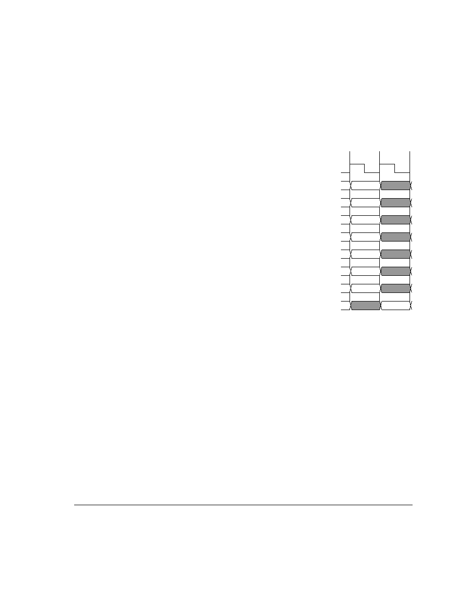
Tightly-Coupled Memories
ARM DDI 0244C
Copyright © 2003 ARM Limited. All rights reserved.
17-5
The TCM interface drives its outputs in the Execute stage of the ARM1026EJ-S
pipeline. This is shown in Figure 17-1 in which all control, address, and external stall
and DMA requests are driven in the first cycle of the diagram. All read data must be
driven in the cycle following, which corresponds to the Memory stage.
Figure 17-1 TCM interface timing
The TCM interface enables maximum design flexibility. A system operates the SRAM
on the falling edge of the clock that drives the ARM1026EJ-S logic. This design
balances the control and address outputs, as well as the data return path, by allowing the
SRAM a full cycle for performing its read or write accesses from falling clock edge to
falling clock edge.
RWBL
RnRW
RCS
CLK
E
M
RWPAR
RWAIT
RRD
RWD
RADDR

Tightly-Coupled Memories
17-6
Copyright © 2003 ARM Limited. All rights reserved.
ARM DDI 0244C
The TCMs perform 8-bit, 16-bit, 32-bit, and 64-bit read and write operations. In write
operations, the TCM interface exports byte write enables. Each chip select and byte
enable maps to an explicit byte lane for the read and write data buses. Table 17-2 shows
the mapping that must be used when connecting the TCM interface.
17.2.3
TCM wait state indicator
In addition to the the standard SRAM signals, the TCM interface includes a wait
indicator. If the TCM cannot service a request in a single cycle, it must assert a wait
signal to inform the ARM1026EJ-S processor that the TCM data is not available for
reads, or that the write requires multiple cycles. Depending on the type of operation, the
processor might stall. If a read operation is being performed, and the TCM indicates a
wait state is desired, then the processor stalls until the read data returns. If a write
operation is being performed, a write stall occurs only when the pending write buffer is
filled, or a subsequent read operation is performed during the stall.
The ARM1026EJ-S processor acknowledges the RWAIT stall only if a TCM request
is being presented. If the TCM is disabled, or no TCM request is being made, the
processor ignores the wait signal. A TCM request might be present during the waited
cycle. It is possible for a read or write to be pending on the TCM interface during a
waited cycle. It is also possible for the TCM address and control outputs to change
during the waited cycle. Due to timing restrictions, it is not possible to prevent
unauthorized reads to the TCM.
Table 17-2 TCM mapping of chip select and byte enable mapping
Chip select
Byte lane
Write data
Read data
RCS[0]
RWBL[0]
RWD[7:0]
RRD[7:0]
RWBL[1]
RWD[15:8]
RRD[15:8]
RWBL[2]
RWD[23:16]
RRD[23:16]
RWBL[3]
RWD[31:24]
RRD[31:24]
RCS[1]
RWBL[4]
RWD[39:32]
RRD[39:32]
RWBL[5]
RWD[47:40]
RRD[47:40]
RWBL[6]
RWD[55:48]
RRD[55:48]
RWBL[7]
RWD[63:56]
RRD[63:56]

Tightly-Coupled Memories
ARM DDI 0244C
Copyright © 2003 ARM Limited. All rights reserved.
17-7
17.2.4
TCM pending write buffer
The TCM pending write buffer holds a maximum of three buffered stores. The buffer
can accomodate any sequence of load or store operations to the TCM without
introducing a resource conflict stall to the ARM1026EJ-S processor.
By asserting the external RWAIT input, the TCM RAM controller can introduce stalls
in the ARM1026EJ-S processor.
Note
It is the responsibility of the programmer to use a drain write buffer instruction to drain
the pending write buffers in the ITCM and DTCM before disabling either of the TCM
regions.
17.2.5
DMA interaction with the TCM controller
The TCM controller in the ARM1026EJ-S processor includes a hook to allow a DMA
engine access to the TCM SRAM. The DMA must assert RDMAEN to request the
TCM interface, and this request must always be presented at least one cycle before
using the TCM interface. The pipelining of the DMA request allows the processor to
determine ownership of the bus and grant ownership as early as the cycle immediately
following the request.
TCM ownership is a function of the DMA request signal, RDMAEN, and the request
and stall indicators, RCS and RWAIT, of the TCM controllers. The conditions for
ownership are shown as a state transition diagram. To determine when it is safe to take
ownership of the TCM SRAM interface, DMA engines built to access the TCM SRAM
must obey the arbitration sequence defined by this state machine. Because the
ARM1026EJ-S processor is given priority access to the TCM interface, there are three
possible states indicating ownership:
∑
TCM1, the idle or zero wait state TCM access state. If the TCM controller is not
initiating an access in the TCM1 state, and the DMA engine is requesting, the
DMA engine becomes the next owner.
∑
TCM2, the TCM controller wait state. The TCM2 state is entered only upon
recognition that the external SRAM requires multiple cycles to perform the
memory operation upon a request from the TCM controller. Exiting TCM2 forces
a new evaluation of the requestors for the TCM interface, and the TCM controller
enters the TCM1 or idle state.
∑
DMA, the DMA ownership state. Exiting DMA forces a new evaluation of the
requestors for the TCM interface, and the TCM controller enters the TCM1 or idle
state.
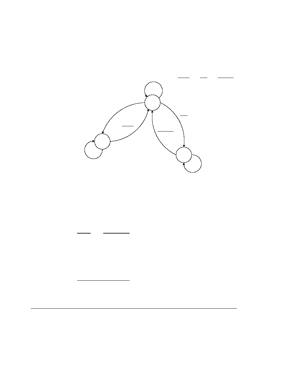
Tightly-Coupled Memories
17-8
Copyright © 2003 ARM Limited. All rights reserved.
ARM DDI 0244C
Figure 17-2 shows the conditions in which ownership of the TCM interface changes.
Figure 17-2 TCM controller and DMA arbitration state diagram
If the ARM1026EJ-S processor and DMA engine request ownership of the TCM
interface in the same cycle, the TCM controller gives priority to the processor. When
the processor activity on the TCM interface is completed, the DMA engine is granted
ownership of the TCM interface. The processor activity on the TCM interface includes
any pending writes in the queue and any wait state activity. When the DMA engine
gains ownership of the TCM interface, it can maintain ownership by keeping
RDMAEN asserted.
Note
RDMAEN must remain deasserted for at least two cycles before being reasserted.
When a DMA engine owns the TCM interface, the ARM1026EJ-S processor forces all
its TCM interface outputs to logic zero. This enables you to use a simple logical OR
function to integrate the DMA SRAM inputs or memory test inputs.
A DMA engine can maintain ownership of the TCM interface indefinitely. Be careful
not to starve the ARM1026EJ-S processor, causing system performance to suffer.
TCM1
TCM2
DMA
RDMAEN
RCS AND RWAIT
RWAIT
RWAIT
RDMAEN
RCS AND RDMAEN
(RCS AND RWAIT) OR (RCS AND RDMAEN)

Tightly-Coupled Memories
ARM DDI 0244C
Copyright © 2003 ARM Limited. All rights reserved.
17-9
17.2.6
TCM memory BIST support
The TCMs are designed to minimize the number of logic gates between the TCM
controller and the RAMs in Memory Built-In Self Test (MBIST) implementations.
When the ARM1026EJ-S processor is held in reset, the TCMs drive logic zeros on all
the TCM output pins to the RAM banks. This enables using OR gates in the signal path
instead of multiplexors, resulting in improved timing for these paths.
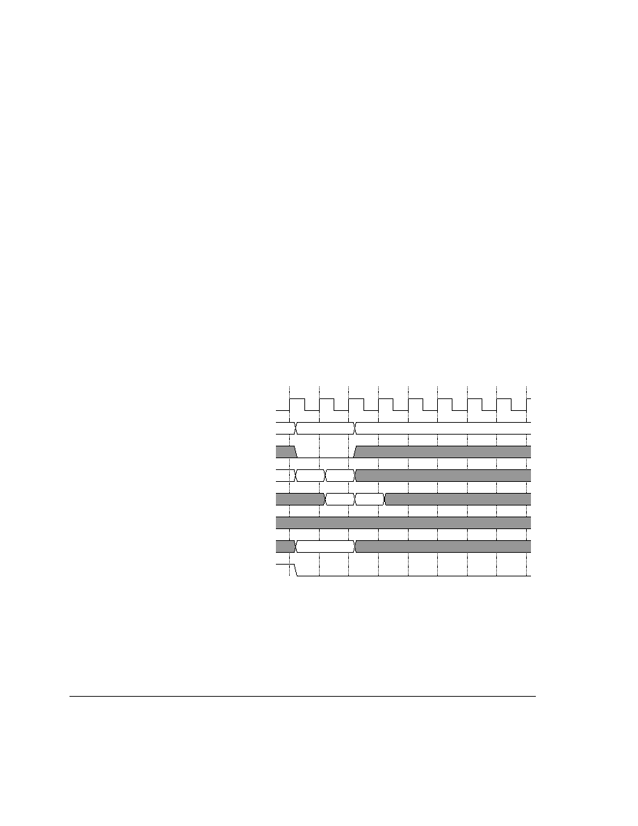
Tightly-Coupled Memories
17-10
Copyright © 2003 ARM Limited. All rights reserved.
ARM DDI 0244C
17.3
Interface timing
This section gives examples of typical TCM interface transfers:
∑
TCM reads with zero wait states
∑
TCM reads with one wait state
∑
TCM reads with four wait states on page 17-11
∑
TCM writes with zero wait states on page 17-12
∑
TCM write with one wait state on page 17-13
∑
TCM write with two wait states on page 17-13
∑
TCM accesses with varying TCM wait states on page 17-14
∑
TCM and DMA interaction on page 17-15.
17.3.1
TCM reads with zero wait states
Figure 17-3 is an example of single-cycle TCM read accesses. RWAIT is never
asserted, and there are no read delays. Read data must be driven in the cycle after the
address and TCM control signals are driven.
Figure 17-3 TCM reads with zero wait states
17.3.2
TCM reads with one wait state
Figure 17-4 on page 17-11 is an example of two-cycle TCM read accesses. RWAIT
delays the R_B and R_C reads for one cycle. Read data must always be driven in the
cycle after RWAIT is deasserted.
00
RCS[1:0]
RADDR[16:0]
CLK
RnRW
RRD[63:0]
RWD[63:0]
RWBL[7:0]
RWAIT
11
00
B
A
R_A
R_B
00
0
0
7
5
4
6
2
3
1
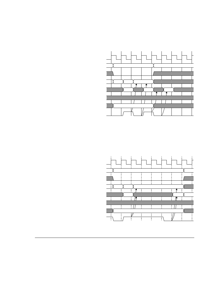
Tightly-Coupled Memories
ARM DDI 0244C
Copyright © 2003 ARM Limited. All rights reserved.
17-11
Figure 17-4 TCM reads with one wait state
17.3.3
TCM reads with four wait states
Figure 17-5 is an example of a five-cycle TCM read access. RWAIT delays the R_B
read for four cycles. Read data must always be driven in the cycle after RWAIT is
deasserted.
Figure 17-5 TCM reads with four wait states
RCS[1:0]
RADDR[16:0]
CLK
RnRW
RRD[63:0]
RWD[63:0]
RWBL[7:0]
RWAIT
11
B
A
R_A
0
00
C
R_C
00
R_B
0
7
5
4
6
2
3
1
RCS[1:0]
RADDR[16:0]
CLK
RnRW
RRD[63:0]
RWD[63:0]
RWBL[7:0]
RWAIT
11
B
A
R_A
R_B
0
C
R_C
00
00
0
7
5
4
6
2
3
1
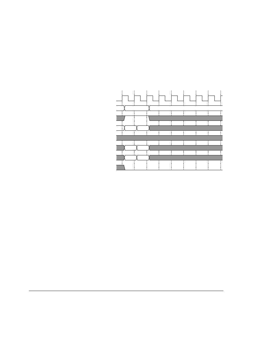
Tightly-Coupled Memories
17-12
Copyright © 2003 ARM Limited. All rights reserved.
ARM DDI 0244C
17.3.4
TCM writes with zero wait states
Figure 17-6 is an example of single-cycle TCM write accesses. RWAIT is never
asserted, and there are no write delays. Write data must be driven in the same cycle as
the address and the TCM control signals.
Figure 17-6 TCM writes with zero wait states
RCS[1:0]
RADDR[16:0]
CLK
RnRW
RRD[63:0]
RWD[63:0]
RWBL[7:0]
RWAIT
B
A
00
00
01/10/11
W_A
W_B
Valid
Valid
00
0
7
5
4
6
2
3
1
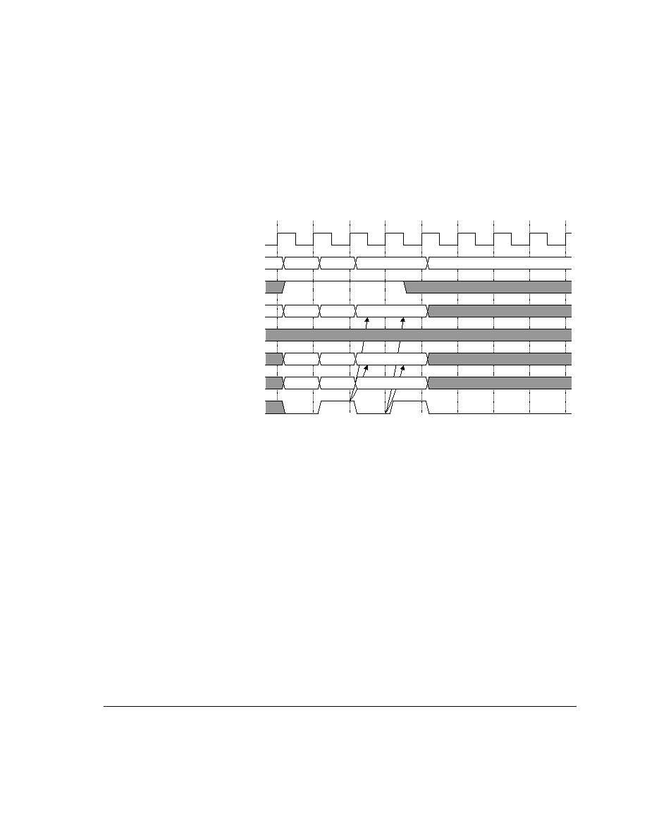
Tightly-Coupled Memories
ARM DDI 0244C
Copyright © 2003 ARM Limited. All rights reserved.
17-13
17.3.5
TCM write with one wait state
Figure 17-7 is an example of a two-cycle TCM write access. RWAIT extends the
completion of both the W_B and W_C writes for one cycle each. Write data must be
driven in the same cycle as the address and the TCM control signals.
Figure 17-7 TCM writes with one wait state
17.3.6
TCM write with two wait states
Figure 17-8 on page 17-14 is an example of a three-cycle TCM write access. RWAIT
extends the completion of both the W_B and W_C writes for two cycles each. Write
data must be driven in the same cycle as the address and TCM control signals.
RCS[1:0]
RADDR[16:0]
CLK
RnRW
RRD[63:0]
RWD[63:0]
RWBL[7:0]
RWAIT
B
A
W_A
W_B
Valid
Valid
01/10/11
00
01/10/11
01/10/11
W_C
Valid
00
C
0
7
5
4
6
2
3
1
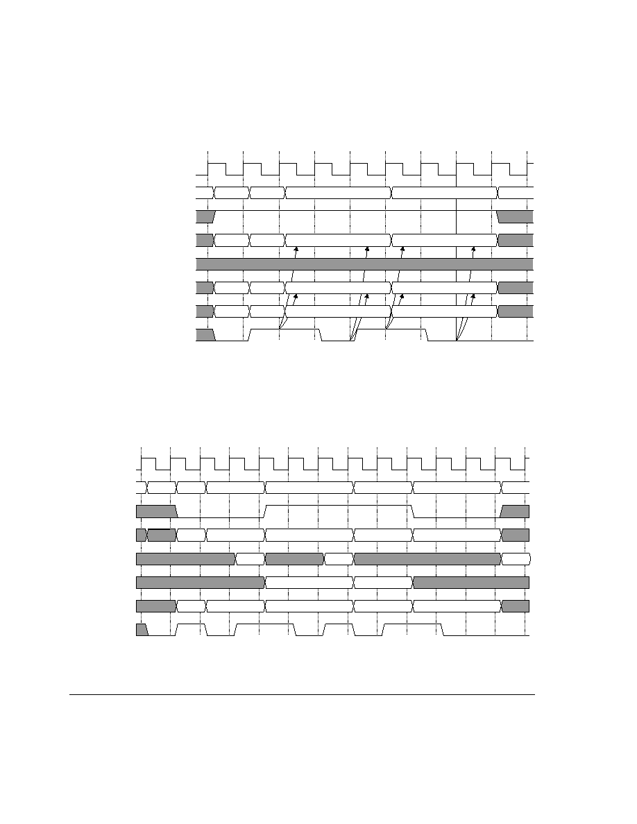
Tightly-Coupled Memories
17-14
Copyright © 2003 ARM Limited. All rights reserved.
ARM DDI 0244C
Figure 17-8 TCM writes with two wait states
17.3.7
TCM accesses with varying TCM wait states
Figure 17-9 shows a mix of read and write transfers with wait states of different lengths.
The lengths of wait states are often transfer-dependent.
Figure 17-9 TCM reads and writes with wait states of varying length
RCS[1:0]
RADDR[16:0]
CLK
RnRW
RRD[63:0]
RWD[63:0]
RWBL[7:0]
RWAIT
01/10/11 01/10/11
00
01/10/11
01/10/11
00
B
A
C
D
Valid
Valid
Valid
Valid
W_A
W_B
W_C
W_D
0
7
5
4
6
2
3
1
8
00
00
RCS[1:0]
RADDR[16:0]
CLK
RnRW
RRD[63:0]
RWD[63:0]
RWBL[7:0]
RWAIT
R_B
R_A
E
D
C
11
11
B
A
01/10/11
01/10/11
00
11
R_E
W_C
W_D
Valid
Valid
0
0
0
0
9
5
4
8
2
3
1
11
6
7
10
12
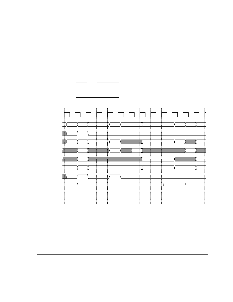
Tightly-Coupled Memories
ARM DDI 0244C
Copyright © 2003 ARM Limited. All rights reserved.
17-15
17.3.8
TCM and DMA interaction
Figure 17-10 shows the DMA engine attempting to gain ownership of the TCM
interface during a sequence of transfers initiated by the ARM1026EJ-S processor.
When the DMA engine gains ownership, the ARM1026EJ-S processor drives the
ARM1026EJ-S outputs to logic zeros.
Note
For the DMA engine to gain and hold access to the TCM SRAM, RDMAEN must be
driven LOW for at least two cycles between separate requests.
Figure 17-10 TCM and DMA interaction
01/10/11
R_E
E
00
00
11
CLK
11
0
1
2
3
4
5
6
7
8
9
10
12
00
0
W_B
0
0
R_C
R_D
R_A
0
D
00
00
11
11
11
C
RCS[1:0]
RADDR[16:0]
RnRW
RRD[63:0]
RWD[63:0]
RWBL[7:0]
RWAIT
B
A
RDMAEN
Interface
owner
State
TCM
TCM
TCM
TCM
TCM
TCM
TCM
DMA
DMA
DMA
TCM
TCM
DMA
TCM1 TCM2
DMA
DMA
DMA TCM1 TCM1
TCM1 TCM1 TCM2 TCM1
TCM1
DMA
0
0
0
0
0
Valid

Tightly-Coupled Memories
17-16
Copyright © 2003 ARM Limited. All rights reserved.
ARM DDI 0244C
17.4
TCM parity
The parity generator is an odd-parity circuit that produces parity bits on a per-byte basis.
If a byte has an even number of 1s, the parity generator appends another 1 to the byte
to produce a nine-bit code word that has an odd number of 1s. Parity generation is not
configurable.
Because the ARM1026EJ-S processor does not provide parity error detection, storing
and handling the parity bit information is the responsibility of the system designer. If
parity error detection is not required, the parity outputs can remain unconnected.
17.4.1
ITCM parity interface
Parity bit generation is provided for every data byte written to the ITCM. Table 17-3
lists the ITCM data bytes and their parity bits.
Table 17-3 ITCM parity interface
Data byte
Parity bit
I/O
IRWD[63:56]
IRWPAR[7]
O
IRWD[55:48]
IRWPAR[6]
O
IRWD[47:40]
IRWPAR[5]
O
IRWD[39:32]
IRWPAR[4]
O
IRWD[31:24]
IRWPAR[3]
O
IRWD[23:16]
IRWPAR[2]
O
IRWD[15:8]
IRWPAR[1]
O
IRWD[7:0]
IRWPAR[0]
O

Tightly-Coupled Memories
ARM DDI 0244C
Copyright © 2003 ARM Limited. All rights reserved.
17-17
17.4.2
DTCM parity interface
Parity bit generation is provided for every byte written in the DTCM. Table 17-4 lists
the DTCM data bytes and their parity bits.
Table 17-4 DTCM parity interface
Data byte
Parity bit
I/O
DRWD[63:56]
DRWPAR[7]
O
DRWD[55:48]
DRWPAR[6]
O
DRWD[47:40]
DRWPAR[5]
O
DRWD[39:32]
DRWPAR[4]
O
DRWD[31:24]
DRWPAR[3]
O
DRWD[23:16]
DRWPAR[2]
O
DRWD[15:8]
DRWPAR[1]
O
DRWD[7:0]
DRWPAR[0]
O

Tightly-Coupled Memories
17-18
Copyright © 2003 ARM Limited. All rights reserved.
ARM DDI 0244C

ARM DDI 0244C
Copyright © 2003 ARM Limited. All rights reserved.
18-1
Chapter 18
Vectored Interrupt Controller Port
This chapter describes the ARM1026EJ-S Vectored Interrupt Controller (VIC) port. It
contains the following sections:
∑
About vectored interrupt controllers on page 18-2
∑
About the VIC port on page 18-3
∑
Timing of the VIC port on page 18-4.

Vectored Interrupt Controller Port
18-2
Copyright © 2003 ARM Limited. All rights reserved.
ARM DDI 0244C
18.1
About vectored interrupt controllers
An interrupt controller is a peripheral that handles multiple interrupt sources. Features
usually found in an interrupt controller are:
∑
multiple interrupt inputs, one for each interrupt source
∑
one interrupt request output for the processor interrupt request input
∑
software maskable interrupt requests
∑
prioritization of interrupt sources for interrupt nesting.
With an interrupt controller that has these features, software is still required to:
∑
determine which interrupt source is requesting service
∑
determine where the service routine for that interrupt source is loaded.
A vectored interrupt controller does both things in hardware. It supplies the starting
address (vector address) of the service routine corresponding to the highest priority
requesting interrupt source.
The ARM1026EJ-S VIC port provides the necessary interface to connect to an external
VIC such as the PL192. The PL192 VIC is an AMBA-compliant, SoC peripheral
developed and tested for use in ARM1026EJ-S designs.

Vectored Interrupt Controller Port
ARM DDI 0244C
Copyright © 2003 ARM Limited. All rights reserved.
18-3
18.2
About the VIC port
The VIC port enables the ARM1026EJ-S processor to read the vector address as part of
the IRQ interrupt entry. The processor takes a vector address from the VIC port
interface instead of the normal address,
0x00000018
, or the high vector address,
0xFFFF0018
.
Hardware relocation of the IRQ vector address eliminates the need for an interrupt
handler to determine the source of an interrupt and branching to a routine to handle it.
Setting the VE bit in the CP15 c1 Control Register enables the processor to read the IRQ
vector address from the VIC port.
Note
The ARM1026EJ-S processor does not support hardware relocation of the FIQ vector
address.
Table 18-1 lists the VIC port signals.
IRQACK and IRQADDRV together implement a four-phase handshake between the
ARM1026EJ-S processor and an external VIC. For more details, see Timing of the VIC
port on page 18-4.
Table 18-1 VIC port signals
Signal
I/O
Description
nFIQ
I
Active-LOW fast interrupt request signal. Synchronous to CLK.
nIRQ
I
Active-LOW normal (IRQ) interrupt request signal.
Synchronous to CLK.
IRQACK
O
Active-HIGH IRQ acknowledge. Indicates to external VIC that
processor is ready to read IRQADDR[31:2].
IRQADDRV
I
Active-HIGH valid signal for the IRQ interrupt vector address.
Indicates to processor that IRQADDR bus is valid, and it is safe
for the processor to sample it.
IRQADDR[31:2]
I
IRQ interrupt vector address. Holds address of first ARM state
instruction in IRQ handler.
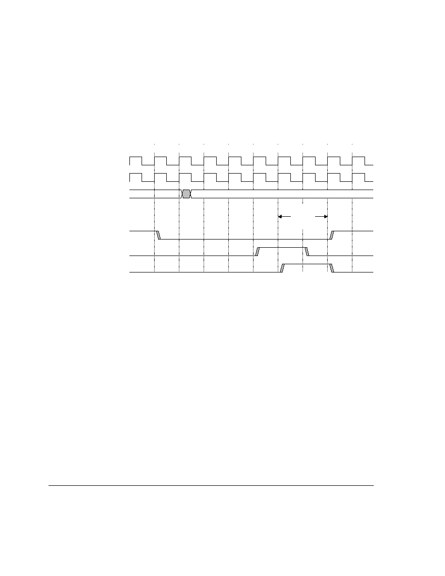
Vectored Interrupt Controller Port
18-4
Copyright © 2003 ARM Limited. All rights reserved.
ARM DDI 0244C
18.3
Timing of the VIC port
Figure 18-1 shows a timing example of VIC port operation with CLK and HCLK
running at the same frequency.
Figure 18-1 VIC port timing example with HCLK:CLK = 1:1
In Figure 18-1, the processor detects that nIRQ is active and asserts IRQACK at B6 to
indicate that it is is ready to service the interrupt request. The time that the processor
takes to respond to nIRQ depends on the current processor state. When the VIC detects
that IRQACK is active, it asserts IRQADDRV at B7 to indicate that the value on the
IRQADDR bus is stable.
When the processor detects that IRQADDRV is active, it samples IRQADDR[31:2] at
B8 and then deasserts IRQACK. When the VIC detects that IRQACK is low, it
deasserts IRQADDRV. If there are no higher priority interrupt requests pending, the
VIC also deasserts nIRQ. The processor samples nIRQ only while IRQADDRV is
inactive.
To prevent a higher-priority interrupt request from changing IRQADDR, the VIC does
not change the value on IRQADDR[31:2] until after the processor deasserts IRQACK
If the processor is running at a multiple of the bus clock frequency, the IRQACK and
IRQADDRV handshake protocol still applies. However, there can be several processor
clock cycles between IRQACK assertion by the processor and IRQADDRV assertion
by the VIC.
Figure 18-2 on page 18-5 shows a timing example of VIC port operation with CLK
running at twice the speed of HCLK.
CLK
HCLK
IRQADDR[31:2]
B1
B2
B3
B4
B5
B6
B7
B8
B9
B10
IRQ vector address
Vector
address
stable
nIRQ
IRQACK
IRQADDRV
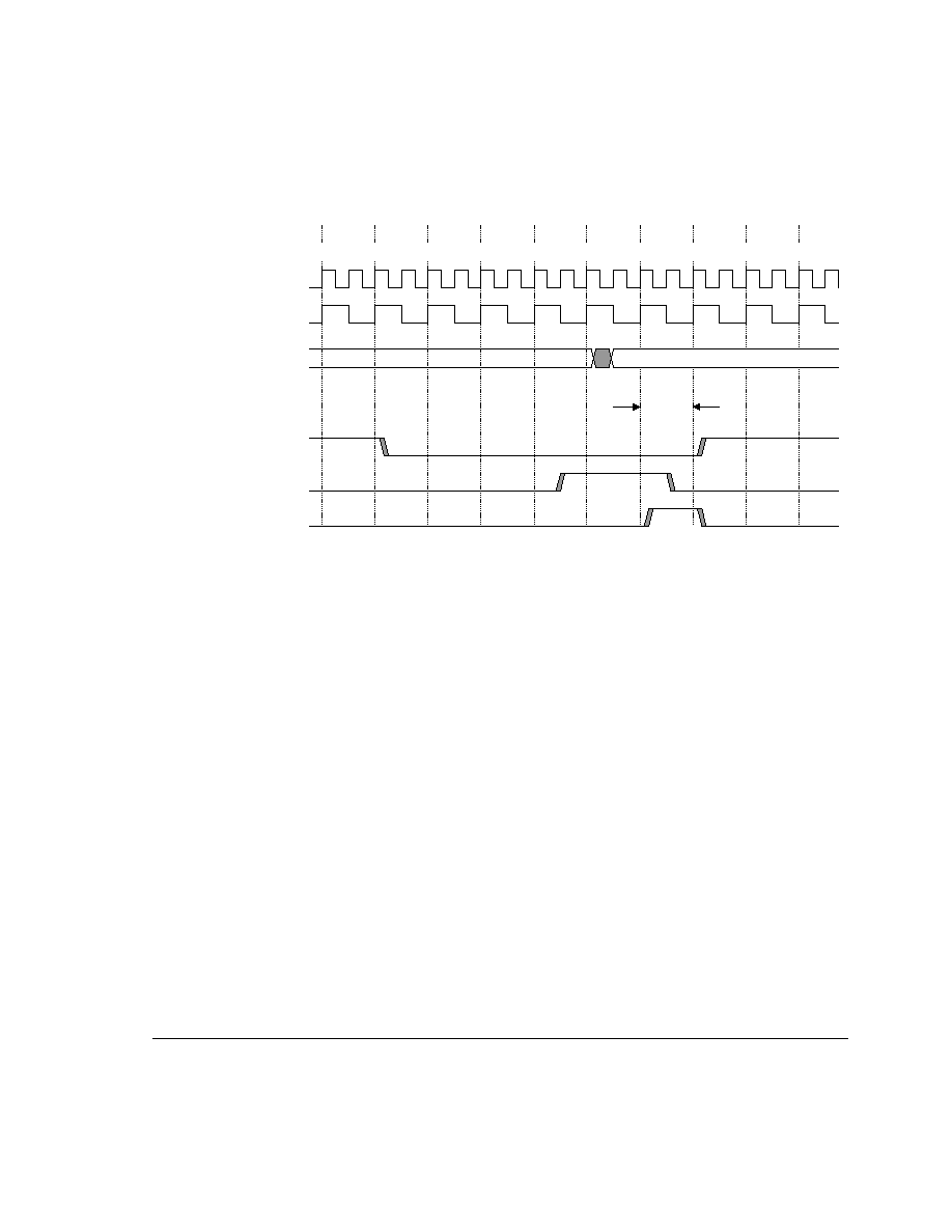
Vectored Interrupt Controller Port
ARM DDI 0244C
Copyright © 2003 ARM Limited. All rights reserved.
18-5
Figure 18-2 VIC port timing example with HCLK:CLK = 2:1
Because the processor clock is running at twice the speed of the bus clock, the
IRQACK response from the processor is valid at P10, earlier than when the processor
and bus clocks are the same.
After the IRQ vector address is generated and IRQACK is detected active, the VIC
asserts IRADDRV at B7. The processor then samples IRQADDR[31:2] at P14 and
deasserts IRQACK.
When the VIC detects that IRQACK is low, it deasserts IRQADDRV, and if no
higher-priority interrupt requests are pending, deasserts nIRQ.
IRQADDR[31:2]
B1
B2
B3
B4
B5
B6
B7
B8
B9
B10
CLK
HCLK
IRQ vector address
P2
P6
P4
P8
P10
P14
P12
P16
P18
Vector
address
stable
nIRQ
IRQACK
IRQADDRV

Vectored Interrupt Controller Port
18-6
Copyright © 2003 ARM Limited. All rights reserved.
ARM DDI 0244C

ARM DDI 0244C
Copyright © 2003 ARM Limited. All rights reserved.
19-1
Chapter 19
Power Management
This chapter describes power management in the ARM1026EJ-S processor. It contains
the following section:
∑
About power management on page 19-2
∑
Wait for interrupt mode on page 19-3
∑
Leakage control on page 19-5.

Power Management
19-2
Copyright © 2003 ARM Limited. All rights reserved.
ARM DDI 0244C
19.1
About power management
The ARM1026EJ-S processor provides two power management facilities:
∑
Wait for interrupt mode on page 19-3
∑
Leakage control on page 19-5.
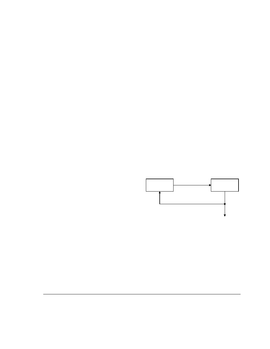
Power Management
ARM DDI 0244C
Copyright © 2003 ARM Limited. All rights reserved.
19-3
19.2
Wait for interrupt mode
The wait for interrupt instructions put the ARM1026EJ-S processor into a low-power
state:
MCR p15, 0, Rd, c7, c0, 4
MCR p15, 0, Rd, c15, c8, 2
Either of these instructions switches the processor into a low-power state until an
interrupt (IRQ or FIQ) or a debug request (EDBGRQ) occurs.
In wait for interrupt mode, all internal clocks can be stopped. The switch into the
low-power state is delayed until all write buffers are drained, and the memory system
is in a quiescent state.
Assertion of the STANDBYWFI signal indicates the switch into a low-power state. If
STANDBYWFI is asserted, then it is guaranteed that all of ARM1026EJ-S external
interfaces (AHB, TCM, and external coprocessor) are in an idle state. You can use
STANDBYWFI to shut down clocks to the ARM1026EJ-S processor and to other
system blocks that do not have to be clocked when the ARM1026EJ-S processor is idle.
Figure 19-3 on page 19-4 shows a user-implemented system clock control block that
uses STANDBYWFI to control the ARM1026EJ-S and system clocks.
Figure 19-1 Using STANDBYWFI to control system clocks
ARM1026EJ-S
processor
Clock
control
STANDBYWFI
To other
system blocks
CLK

Power Management
19-4
Copyright © 2003 ARM Limited. All rights reserved.
ARM DDI 0244C
The STANDBYWFI signal is deasserted in the cycle following an interrupt or a debug
request. It is guaranteed that no form of access on any external interface is started until
the cycle after STANDBYWFI is deasserted. Figure 19-2 shows the deassertion of the
STANDBYWFI signal after an IRQ interrupt.
Figure 19-2 Deassertion of STANDBYWFI after an IRQ interrupt
When the processor enters a low-power state, all of the main internal clocks can be
stopped. However, the processor is active if DBGTCKEN is asserted. This means that
you can safely stop CLK if STANDBYWFI is HIGH and DBGTCKEN is LOW.
Figure 19-3 shows an example of user-implemented system logic for stopping the main
ARM1026EJ-S clock during wait for interrupt.
Figure 19-3 Using STANDBYWFI to control ARM1026EJ-S clocks
The nature of the nFIQ, nIRQ, and EDBGRQ signals enables them to be registered
prior to being used in the gating logic.
STANDBYWFI
nIRQ
CLK
nFIQ
EDBGRQ
nIRQ
DBGTCKEN
STANDBYWFI
FCLK
FCLK = free-running clock
CLK = ARM processor clock
RST
EN
CLK
HRESETn

Power Management
ARM DDI 0244C
Copyright © 2003 ARM Limited. All rights reserved.
19-5
19.3
Leakage control
The ARM1026EJ-S design is partitioned so that the SRAM blocks that are used for the
caches and the MMU can be powered down under certain conditions.
When the RAMs are powered down, the RAM outputs to the ARM1026EJ-S cache
controller must be driven either HIGH or LOW. ARM recommends driving the RAM
outputs LOW. Figure 19-4 shows an example of user-implemented logic to drive the
RAM outputs LOW in power-down.
Figure 19-4 Cache power-down
19.3.1
Cache RAMs
You can safely power down the RAMs for either cache if the cache contains no valid
entries and you first disable it by using the CP15 c1 Control Register. While a cache is
disabled, only CP15 c7 cache maintenance instructions can cause the cache RAMs to
be accessed. You must not re-enable the cache or execute these instructions while any
of the cache RAMs are powered down.
19.3.2
MMU RAMs
You can safely power down the RAM used to implement the MMU if the MMU
contains no valid entries and you first disable it by using the CP15 c1 Control Register.
While the MMU is disabled, only CP15 c8 TLB maintenance instructions and CP15 c15
MMU test/debug instructions can cause the MMU RAM to be accessed. You must not
re-enable the MMU or execute these instructions while the MMU RAM is powered
down.
Cache
controller
Power-down
enable
Cache
RAMs
ARM1026EJ-S processor

Power Management
19-6
Copyright © 2003 ARM Limited. All rights reserved.
ARM DDI 0244C

ARM DDI 0244C
Copyright © 2003 ARM Limited. All rights reserved.
20-1
Chapter 20
Design for Test
This chapter describes the Design For Test (DFT) features of the ARM1026EJ-S
processor and describes how to integrate the DFT features into a System on a Chip
(SoC). This chapter contains the following sections:
∑
ARM1026EJ-S processor on page 20-2
∑
Test signal connections on page 20-10
∑
MBIST on page 20-13.
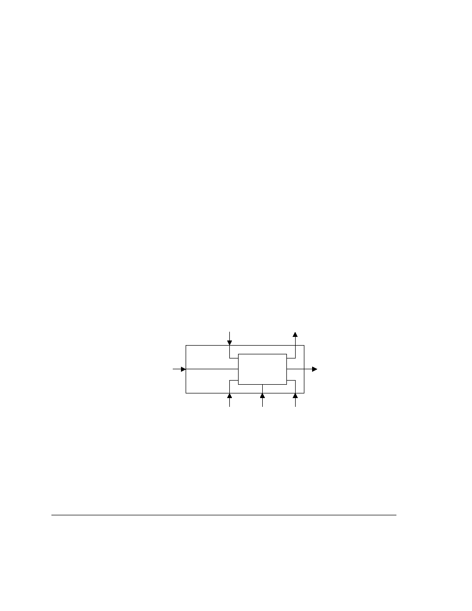
Design for Test
20-2
Copyright © 2003 ARM Limited. All rights reserved.
ARM DDI 0244C
20.1
ARM1026EJ-S processor
Except for reset, the ARM1026EJ-S processor is a fully synchronous muxD flip-flop
macrocell. It contains one internal clock domain controlled by the CLK pin.
20.1.1
Test wrapper
The test wrapper provides a single serial scan ring around the entire periphery of the
processor. You can use the test wrapper to apply test vectors with minimal external pin
control. The test wrapper enables test control and observation of the core from the ports
as well as control and observation of the external logic surrounding the processor.
Wrapper cells can be dedicated or shared. Shared wrapper cells are functional flip-flops
that are also used as wrapper cells. Shared wrapper cells must be registered inputs or
outputs. Dedicated wrapper cells are defined in the RTL. Connect the dedicated
wrapper cells into the test wrapper along with the shared wrapper cells during the scan
insertion portion of the synthesis flow. The functional clock, CLK, drives the wrapper
cells. This flow works in the ARM environment, but it requires a list of the shared
wrapper cells. The format of these paths might change depending on the tool used for
synthesis and how the tool is used. If the scan insertion tool can read the wrapper cell
names, then there is no problem with scan insertion of the wrapper using the ARM flow.
Figure 20-1 shows the structure of a dedicated input wrapper cell.
Figure 20-1 Dedicated input wrapper cell
Figure 20-2 on page 20-3 shows the structure of a dedicated output wrapper cell.
Peripheral logic
ARM1026EJ-S processor
Scan input
Scan output
Functional path
Scan enable
CLK
MUXINSEL
SI
IN
CLK
SO
SE
OUT
SEL
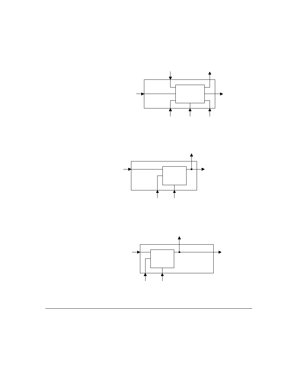
Design for Test
ARM DDI 0244C
Copyright © 2003 ARM Limited. All rights reserved.
20-3
Figure 20-2 Dedicated output wrapper cell
Figure 20-3 shows the structure of a shared input wrapper cell.
Figure 20-3 Shared input wrapper cell
Figure 20-4 shows the structure of a shared output wrapper cell.
Figure 20-4 Shared output wrapper cell
Functional path
Peripheral logic
ARM1026EJ-S processor
Scan input
Scan output
Scan enable
CLK MUXOUTSEL
IN
SI
CLK
SO
SE
OUT
SEL
Peripheral logic
ARM1026EJ-S processor
Scan output
Functional input
Scan input CLK
D
SDI
CLK
Q
Peripheral logic
ARM1026EJ-S processor
Scan output
Functional output
Scan input CLK
D
SDI
CLK
Q

Design for Test
20-4
Copyright © 2003 ARM Limited. All rights reserved.
ARM DDI 0244C
The test wrapper has six scan chains with a total of 870 wrapper scan cells. The wrapper
chain consists of both shared and dedicated wrapper cells and is segmented into shorter
scan chains that can be used for both external and internal testing. The wrapper insertion
script creates two scan enables (see WSEI and WSEO on page 20-6). The input bus to
the wrapper scan chains is WSI, and the output bus is WSO. There is a wrapper cell
connected to every input and output functional port with the exception of the clock port
and memories.
Note
There are no gates at the processor outputs. While the processor is being tested, the
outputs ripple as data is clocked through the wrapper chain. If necessary, you can add
external gates to the outputs.
The dedicated test cells require control signals to differentiate between internal testing,
external testing, and functional mode. Table 20-1 shows how MUXINSEL and
MUXOUTSEL select mode of operation.
20.1.2
Wrapper segmentation
The ARM1026EJ-S wrapper has three segments:
∑
one segment is connected to the coprocessor interface
∑
one segment is connected to the ETM interface
∑
one segment is connected to the AHB interface.
Each segment divided into a wrapper chain that uses WSEI and a wrapper chain that
uses WSEO. See Figure 20-5 on page 20-5.
Table 20-1 Selecting mode of operation of dedicated wrapper cells
MUXINSEL
MUXOUTSEL
0
0
Functional mode.
0
1
External test mode.
Wrapper input cells can observe data from peripheral logic.
Wrapper data present on ARM1026EJ-S port.
1
0
Internal test mode.
Dedicated input wrapper cells inward-facing to control of ARM1026EJ-S inputs.
Functional data present on ARM1026EJ-S port.
1
1
Unused.
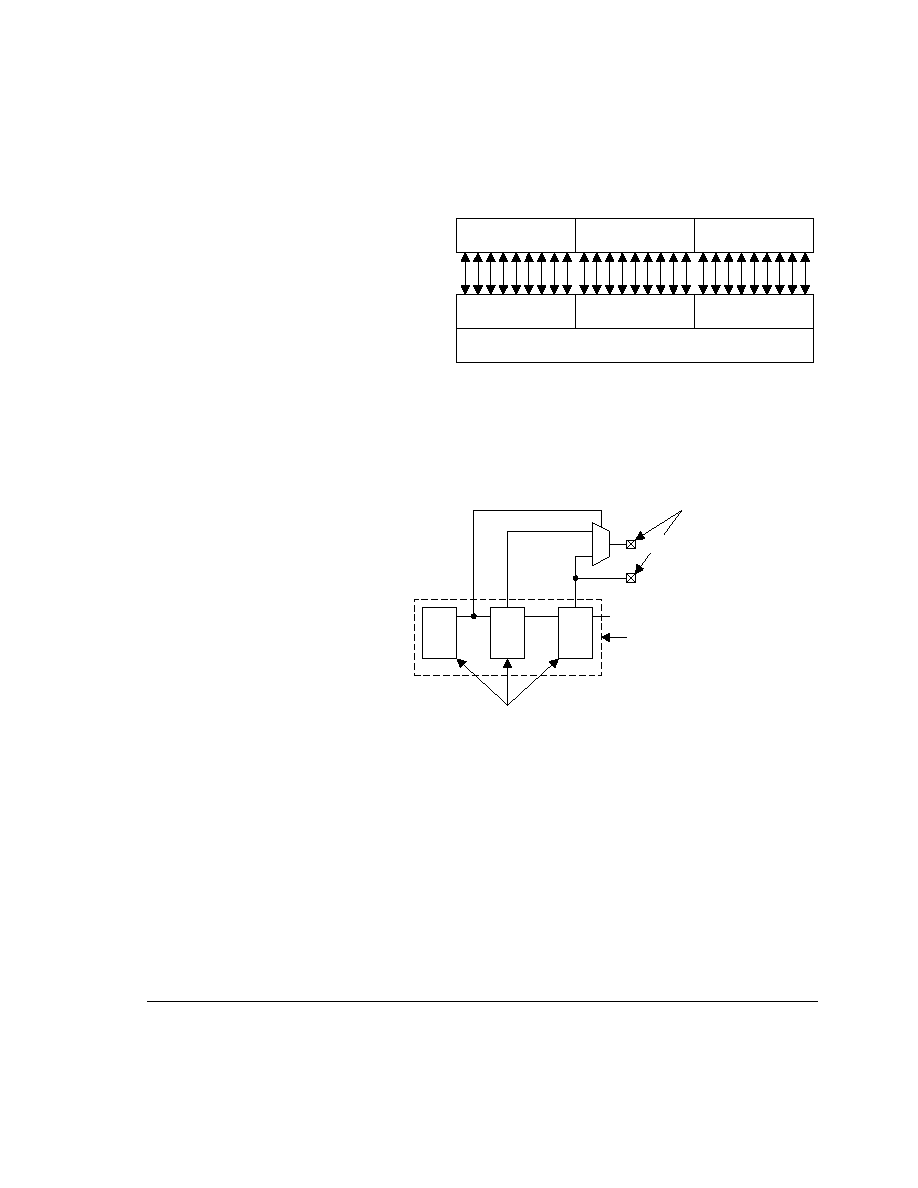
Design for Test
ARM DDI 0244C
Copyright © 2003 ARM Limited. All rights reserved.
20-5
Figure 20-5 Wrapper segments
The shared AHB wrapper cells in the UDL segment of the wrapper chain are connected
to the output ports of the data bus through multiplexors as Figure 20-6 shows. All logic
outside of the dashed box is tested only in external test mode.
Figure 20-6 HWDATA bus output ports
The shared AHB wrapper cells in the UDL segment of the wrapper chain are connected
to the input ports of the D bus through multiplexors as Figure 20-7 on page 20-6 shows.
All logic outside of the dashed box is tested only in external test mode.
User-defined logic
Coprocessor
ETM10
ETM interface
Coprocessor
interface
AHB interface
ARM1026EJ-S processor
ARM1026EJ-S output ports
HWDATAD/I[63:32]
HWDATAD/I[31:0]
Tested during internal test
Shared wrapper cells

Design for Test
20-6
Copyright © 2003 ARM Limited. All rights reserved.
ARM DDI 0244C
Figure 20-7 HRDATA bus input ports
You can concatenate the wrapper scan chains as required by wiring the WSO of one
scan chain to the WSI of another scan chain. Table 20-2 shows the lengths of the scan
chains.
WSEI and WSEO
The wrapper contains two scan-enable signals:
WSEI
Wrapper scan-enable input. WSEI connects only to the wrapper cells
adjacent to the functional inputs.
WSEO
Wrapper scan-enable output. WSEO connects only to wrapper cells
adjacent to the functional outputs.
ARM1026EJ-S input ports
HRDATAD/I[31:0]
HRDATAD/I[63:32]
Tested during internal test
Shared wrapper cells
Table 20-2 Wrapper scan chains
Scan chain
Function
Number of flip-flops in chain
0
AHB-in
237
1
CP-in
86
2
ETM-in
1
3
AHB-out
219
4
CP-out
102
5
ETM-out
225
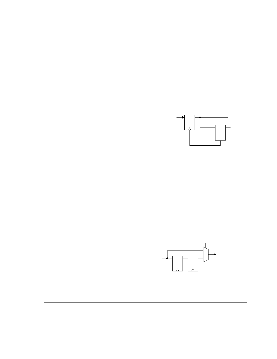
Design for Test
ARM DDI 0244C
Copyright © 2003 ARM Limited. All rights reserved.
20-7
In designs that do not require separate scan enables, you can tie WSEI and WSEO
together as one wrapper scan-enable signal.
WSO
The AHB segment of the scan chain has two wrapper outputs as Figure 20-8 shows.
When there is one wrapper chain, WSO is the output. There is a
2 latched output called
WSON for connecting the wrapper chain to scan chains in other clock domains.
Figure 20-8 Wrapper falling-edge logic
20.1.3
Clock gating
The clock is not gated in the ARM1026EJ-S processor. It can be gated externally to turn
off the clock during I
DDQ
test setup or to minimize power consumption while testing
logic other than the ARM1026EJ-S processor. Because there is only one clock domain
in the core, a clock gate would also disable the wrapper.
20.1.4
Reset
The HRESETn and DGBnTRST signals are asynchronous resets that are delivered to
the flip-flops out of a dual flip-flop synchronizer as Figure 20-9 shows. For direct
control of reset during scan testing, the outputs of the flip-flops are blocked if they go
to the reset ports on internal flip-flops.
Figure 20-9 Reset synchronizer
During scan mode, the 0 mux input and the 0 state of the mux select input in Figure 20-9
are not tested.
WSO[0]
Lockup latch
WSON
Last flip-flop in the UDL
wrapper scan chain
HRESETn or DBGnTRST
0
1
Reset to flip-flops
SCANMODE
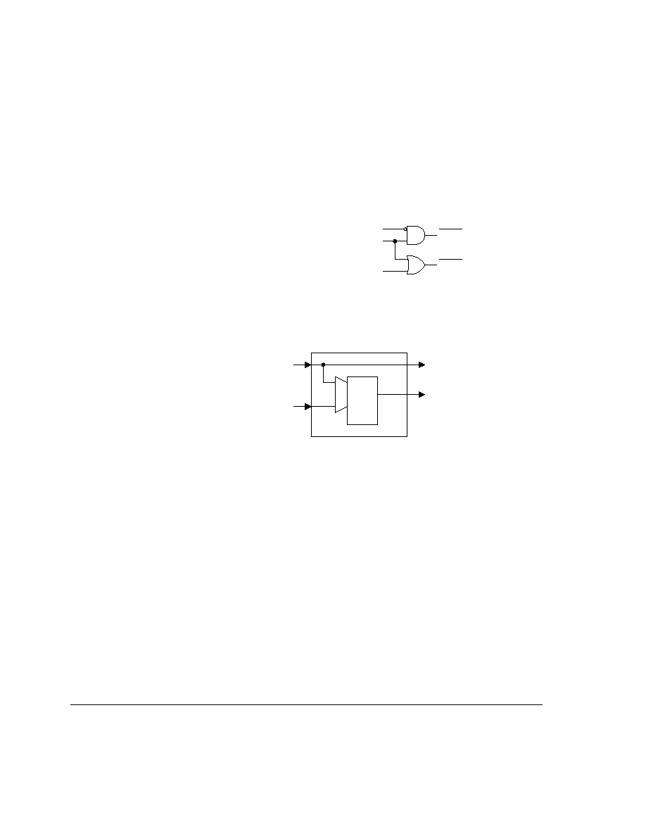
Design for Test
20-8
Copyright © 2003 ARM Limited. All rights reserved.
ARM DDI 0244C
The clock that drives the wrapper also controls the ARM1026EJ-S internal flip-flops.
The RSTSAFE signal enables you to reset the ARM1026EJ-S processor to some extent
during external test mode. As Figure 20-10 shows, RSTSAFE connects only to
flip-flops that are not contained in the wrapper scan chain. While in external test mode,
the HRESETn signal has no effect on the wrapper cells that have reset ports.
Figure 20-10 RSTSAFE signal
The reset signals must be directly connected to a port during test. The wrapper cell for
asynchronous resets contain only an observe register, as Figure 20-11 shows.
Figure 20-11 Reset wrapper cell
RSTSAFE
External test mode
HRESETn or DBGnTRST
to internal flip-flops
Reset
to wrapper flip-flops
Reset
OUT
To next scan cell
To ARM1026EJ-S reset logic
From previous scan cell
HRESETn or DBGnTRST

Design for Test
ARM DDI 0244C
Copyright © 2003 ARM Limited. All rights reserved.
20-9
20.1.5
Test ports
The dedicated test ports in Table 20-3 must be instantiated as specified for internal
testing to operate correctly. Dynamic signals must make single-cycle test timing to the
core logic.
Table 20-3 Test port signals during internal test
Port name
I/O
Type
Description
SCANMODE
I
Static
Prevents asynchronous reset from being controlled by synchronizer
RSTSAFE
I
Static
Resets any core cells that are reset-capable except wrapper cells
SE
I
Dynamic
Scan enable for all internal clock domains. HIGH = shift
SI[55:0]
I
Dynamic
Scan input port
SO[55:0]
O
Dynamic
Scan output port
Wrapper signals
WSEI
I
Dynamic or static
a
Scan enable for all input-dedicated wrapper test cells. HIGH = shift
WSEO
I
Dynamic
Scan enable for all output-dedicated wrapper test cells. HIGH = shift
WSI[5:0]
I
Dynamic
Input ports for wrapper scan chains
WSO[5:0]
O
Dynamic
Output ports for wrapper scan chains
WSON
O
Dynamic
Wrapper output port that changes after falling edge of clock
MUXINSEL
I
Static
Configures dedicated input wrapper cells for functional or test mode
MUXOUTSEL
I
Static
Configures dedicated output wrapper cells for functional or test mode
WMUX[1:0]
I
Static
Unused
SCANMUX[1:0]
I
Static
Unused
CHECKTEST
I
Static
Unused
a. No capture required on inputs during INTEST. Dynamic during EXTEST.

Design for Test
20-10
Copyright © 2003 ARM Limited. All rights reserved.
ARM DDI 0244C
20.2
Test signal connections
This section contains the following test signal connection tables:
∑
Test port connections in internal test mode
∑
Test port connections in functional mode on page 20-11
∑
Test port connections in external test mode on page 20-12.
See Memory test interface on page 20-13 for a description of MBIST connections.
Table 20-4 shows the test port connections for internal test mode.
Table 20-4 Test port connections in internal test mode
Signal
Value
SCANMODE
1
RSTSAFE
0
SE
Connect to external pin
SI[55:0]
Connect to external pins
SO[55:0]
Connect to external pins
WSEI
Connect to external pin or 1
a
a. See WSEI and WSEO on page 20-6.
WSEO
Connect to external pin
MUXINSEL
1
MUXOUTSEL
0
WSI[5:0]
Connect to external pins
WSO or WSON
b
b. WSO or WSON can be connected to another scan
chain if necessary.
Connect to external pin

Design for Test
ARM DDI 0244C
Copyright © 2003 ARM Limited. All rights reserved.
20-11
Table 20-5 shows test port connections for functional mode.
Table 20-5 Test port connections in functional mode
Test signals
Connection
SCANMODE
0
RSTSAFE
0
SE
0
SI[55:0]
0 recommended
SO[55:0]
Gated 0 recommended
WSEI
0
WSEO
0
MUXINSEL
0
MUXOUTSEL
0
WSI[5:0]
0 recommended
WSO[5:0]
Gated 0 recommended
WSON
Gated 0 recommended
MBISTRESETN
0

Design for Test
20-12
Copyright © 2003 ARM Limited. All rights reserved.
ARM DDI 0244C
Table 20-6 shows the test signal connections for external test mode.
Table 20-6 Test port connections in external test mode
Signal
Value
SCANMODE
1
RSTSAFE
1 recommended unless I
DDQ
testing
SE
0
SI[55:0]
0 recommended
SO[55:0]
Gated 0 recommended
WSEI
Connect to external pin
WSEO
Connect to external pin or 1
a
a. See WSEI and WSEO on page 20-6.
MUXINSEL
0
MUXOUTSEL
1
WSI[5:0]
Connect to external pin
WSO[5:0] or WSON
b
b. WSO or WSON can be connected to another scan chain if
necessary.
Connect to external pin
MBISTRAMBYP
Connect to external pin
MBISTRESETN
Connect to external pin
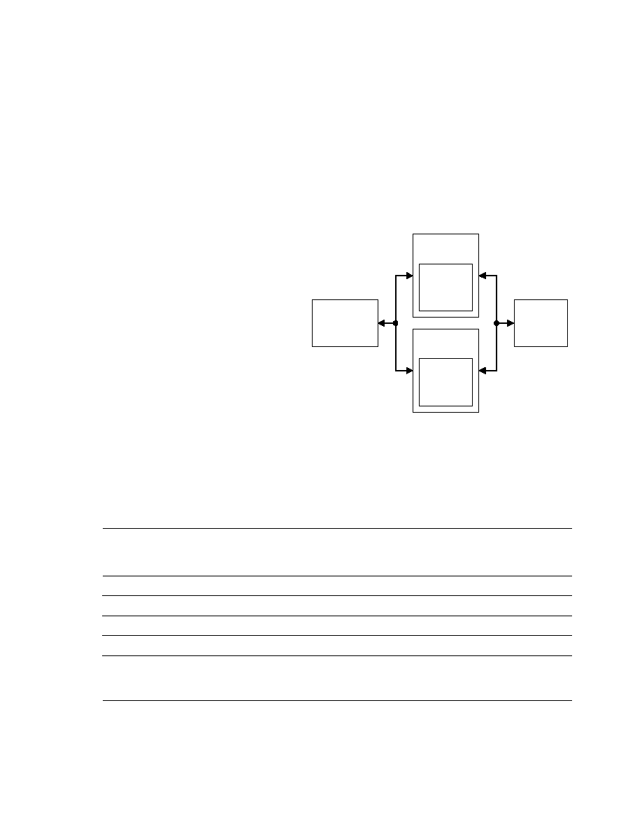
Design for Test
ARM DDI 0244C
Copyright © 2003 ARM Limited. All rights reserved.
20-13
20.3
MBIST
This section describes the array architecture, register definition, address mapping, and
implementation of the ARM1026EJ-S Memory Built-In Self Test (MBIST).
Figure 20-12 shows the high-level organization of the ARM1026EJ-S MBIST.
Figure 20-12 MBIST block diagram
20.3.1
Memory test interface
Table 20-7 summarizes the interface between the MBIST controller and the memory
wrapper.
ARM
processor
MBIST
controller
TCM
dispatch
unit
TCM
wrapper
Memory
wrapper
Memory
dispatch
unit
Table 20-7 MBIST interface in test mode
Signal
I/O Function
Connection
Value in
MBIST test
mode
Value in
functional
mode
MBISTCLKEN
I
MBIST clock gate
External pin and MBIST controller Toggle
0
MTESTON
I
MBIST path enable
External pin and MBIST controller Toggle
0
MBISTDSHIFT
I
Data log shift
External pin and MBIST controller Toggle
0
MBISTSHIFT
I
Instruction shift
External pin and MBIST controller Toggle
0
MBISTDIN
I
Serial data shift in
External pin and MBIST controller Toggle
0

Design for Test
20-14
Copyright © 2003 ARM Limited. All rights reserved.
ARM DDI 0244C
Each dispatch unit connects the MBIST controller to the memory test interface of the
processor. The dispatch unit resides in the memory wrapper. Some cache-read paths in
the wrapper also contain functional path
1 latches to enable timing to be met in
functional mode.
MBISTDOUT[2:0]
During tests, the MBISTDOUT[2] signal indicates failures. This can operate using two
modes, configured using bit 5 of the engine control section of the instruction register. If
bit 5 is set, MBISTDOUT[2] is asserted for a single cycle for each failed compare. If
bit 5 is not set, MBISTDOUT[2] is sticky, and is asserted from the first failure until the
end of the test. At the completion of the test, the MBISTDOUT[1] signal goes HIGH.
MBISTDOUT[0] indicates that an address expire has occurred and enables you to
measure sequential progress through the test algorithms.
MBISTDOUT[2:0]
O
Output status bus
External pin and MBIST controller Strobe
-
MBISTRAMBYP
I
Chip-select block
External pin and MBIST controller 0
0
HRESETn
I
Core reset value
External pin
0
a
Toggle
MBISTRESETN
I
MBIST reset signal
External pin and MBIST controller Toggle
0
b
SCANMODE
I
ATPG signal
External pin and MBIST controller 0
0
SE
I
ATPG signal
External pin and MBIST controller 0
0
MBISTRXTCM[2:0] O
Dispatch unit output bus MBIST controller
-
-
MBISTRXCGR[2:0] O
Dispatch unit output bus MBIST controller
-
-
MBISTTX[10:0]
I
MBIST controller out
MBIST controller
-
-
a. HRESETN must be LOW in MBIST test mode.
b. MBISTRESETN must be LOW in functional mode.
Table 20-7 MBIST interface in test mode (continued)
Signal
I/O Function
Connection
Value in
MBIST test
mode
Value in
functional
mode

Design for Test
ARM DDI 0244C
Copyright © 2003 ARM Limited. All rights reserved.
20-15
MBISTTX[10:0]
Table 20-8 shows how the MBIST controller interacts with the dispatch unit through
the MBISTTX[10:0] interface.
When instruction shift is enabled, data shifts in on bit 1 (AddrInc in normal operation)
and shifts into the instruction scan chain of the dispatch unit. The MBISTTX[10:0]
interface is ARM-specific and intended for use only with the ARM MBIST controller.
Table 20-8 MBISTTX external interface
MBISTTX[10:0]
bit
Description
0
Reset address
1
Increment address
2
Access sacrificial row (used during bang patterns)
3
Invert data/instruction data in
4
Checkerboard data
5
Write data
6
Read data
7
Yfast/nXfast
8
Direction
9
Enable bitmap mode
10
Increment go/nogo dataword selection

Design for Test
20-16
Copyright © 2003 ARM Limited. All rights reserved.
ARM DDI 0244C
MBISTRXCGR[2:0] and MBISTRXTCM[2:0]
Table 20-9 shows how the dispatch units interact with the MBIST controller through
the MBISTRXTCM and MBISTRXCGR interfaces.
The behavior of MBISTRXCGR[2:0] and MBISTRXTCM[2:0] is ARM-specific.
These signals are intended for use only with the ARM MBIST controller.
The address expire signal is set when both address counters expire.
20.3.2
MBIST and ATPG
This section describes MBIST/ATPG considerations.
MBISTRAMBYP
Figure 20-13 on page 20-17 shows the data path for processor cache reads. The
scannable MBIST data register for data compares also controls this path during ATPG
testing and provides an observe path. This is particularly useful when testing the
processor with black-boxed memories. MBISTRAMBYP controls the multiplexor that
selects between cache data and DFT data. ATPG runs performed with black-boxed
memories must constrain MBISTRAMBYP active. The MBIST data compare flip-flop
can also serve as an observe register when performing ATPG RAM tests.
Caution
MBISTRAMBYP is a static signal. Constrain MBISTRAMBYP in ATPG runs.
Table 20-9 MBISTRXCGR[2:0] and MBISTRXTCM[2:0] external interface
MBISTRXCGR or
MBISTRXTCM bit
Description
0
Address expire/instruction data out/fail data out
1
Bitmap stall
2
Nonsticky fail flag
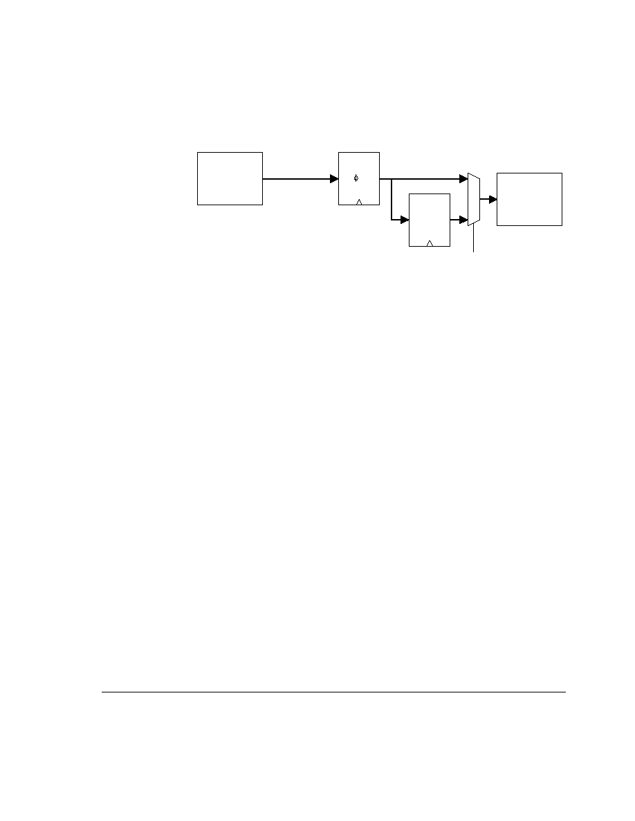
Design for Test
ARM DDI 0244C
Copyright © 2003 ARM Limited. All rights reserved.
20-17
Figure 20-13 ATPG view of read datapath
Scan enable, SE
Preservation of array state is required when performing multiload ATPG runs or when
performing I
DDQ
testing. The ARM MBIST blocks all array chip-select signals with the
SE signal. After performing MBIST tests to initialize the arrays to a desired
background, the ATPG test procedures must assert SE during all test setup cycles in
addition to load/unload. Any clocking during I
DDQ
capture cycles must have array
chip-select signals constrained.
20.3.3
MBIST arrays
The following sections describe the MBIST arrays:
∑
Memory test and chip select
∑
Data-side MBIST arrays on page 20-18
∑
Instruction-side MBIST arrays on page 20-20
∑
MMU MBIST array on page 20-20
∑
TCM MBIST array on page 20-21
∑
Memory test times on page 20-22.
Memory test and chip select
This section describes how each array is enabled by the dispatch unit. Most arrays in
this listing can be tested in parallel. This is accomplished by setting maximum X and Y
address spaces as required for the largest RAMs in each dimension. If the X and Y
address space exceeds the dimension of an array, the address scramble block within the
MBIST wrapper gates the internal chip select of the array.
Cache read data
BIST
data
compare
MBISTRAMBYP
ARM1026EJ-S
processor
Physical RAM
1
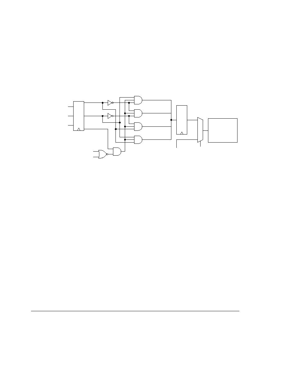
Design for Test
20-18
Copyright © 2003 ARM Limited. All rights reserved.
ARM DDI 0244C
There are architectural four-bit chip-select signals for tag and data RAM arrays as
shown in Figure 20-14. The MBIST tests these arrays serially by assigning their
chip-select bits to the Yaddr space to be gated by the master chip select of the memory
test interface.
Figure 20-14 Chip-select implementation example
Data-side MBIST arrays
The data-side arrays contain four data, four tag, one valid, and one dirty array. There
are four chip-select signals that control the data and tag RAMs. The four chip-select bits
are controlled by appending them to the Yaddr space during MBIST testing. A single
chip-select signal enables the valid and dirty RAMs.
The data RAM exists as four separate 64-bit arrays, each controlled by a chip select. The
tag RAM exists as four separate arrays, one half containing a virtual tag, the other half
holding the physical tag. The tag is 22 bits wide. Addr[12] selects between the physical
and virtual set. The four RAM arrays are selected by TagCS[3:0]. These chip-select
signals are appended to the Y address space during MBIST testing. See Figure 20-15
on page 20-19.
Physical
DCache and
data RAM
Yaddr[4]
Yaddr[5]
DCDATACS[2]
DCDATACS[0]
DCDATACS[1]
DCDATACS[3]
MTESTYADDR[2]
MTESTXADDR[2]
MTESTCE2[3]
MTESTCE[1]
Xaddr[10:8]
Yaddr[10:8]
Functional
path
MTESTON
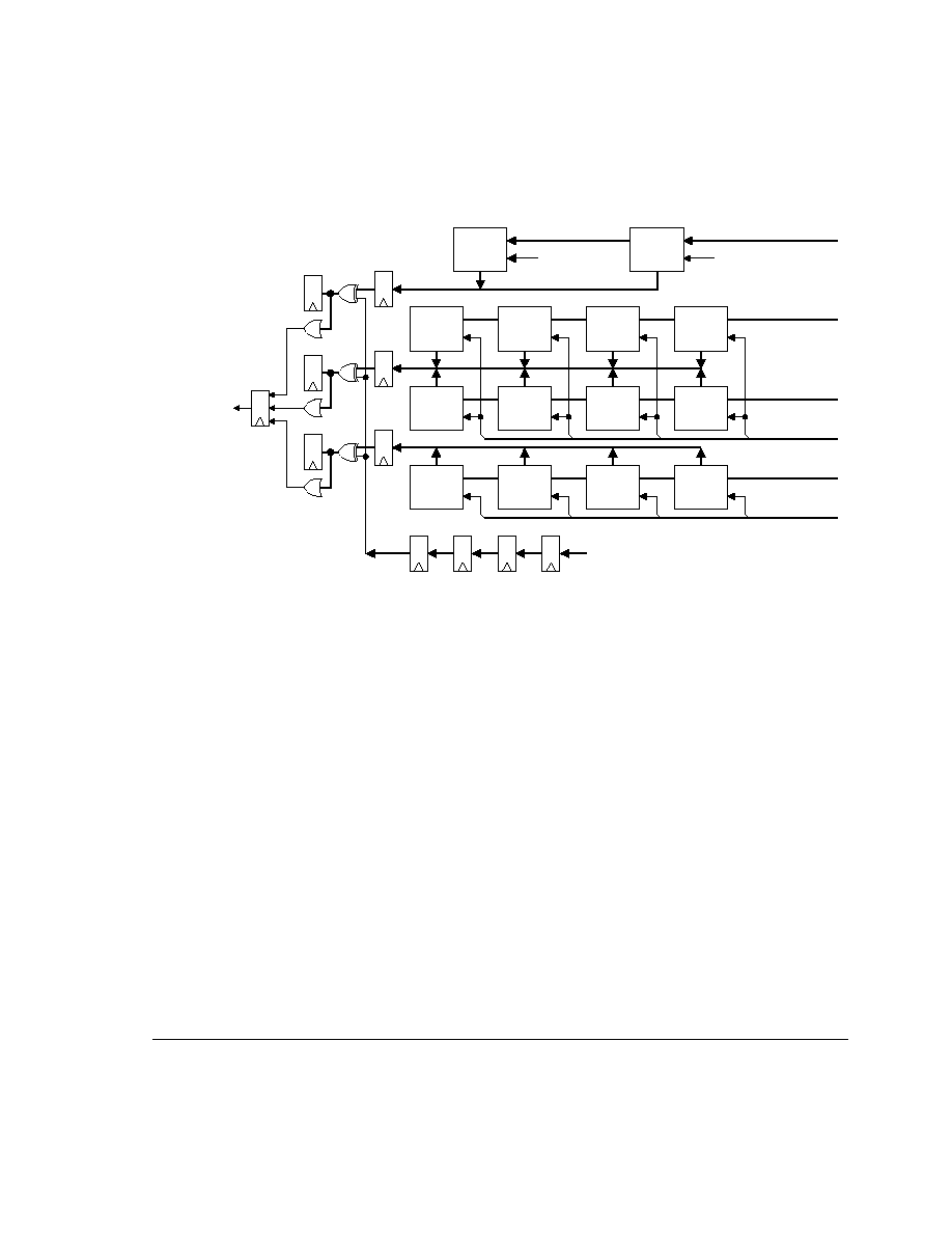
Design for Test
ARM DDI 0244C
Copyright © 2003 ARM Limited. All rights reserved.
20-19
Figure 20-15 Data RAM MBIST arrays
[0]
[1]
[2]
[3]
Dirty
PTAG0
PTAG1
PTAG2
PTAG3
DATA0
Addr[10:0]
Addr[9:0]
Tag CS[3:0]
Addr[10:0]
[0]
[1]
[2]
Data CS[3:0]
[3]
Addr[11:0]
DATA1
DATA2
VTAG2
VTAG3
VTAG0
VTAG1
Valid CS
Dirty CS
DATA3
Valid
24
32
8
64
22
InstrData[3:0]
{16{BistData4[3:0]}}
Fail
Data log and
bitmap support
registers
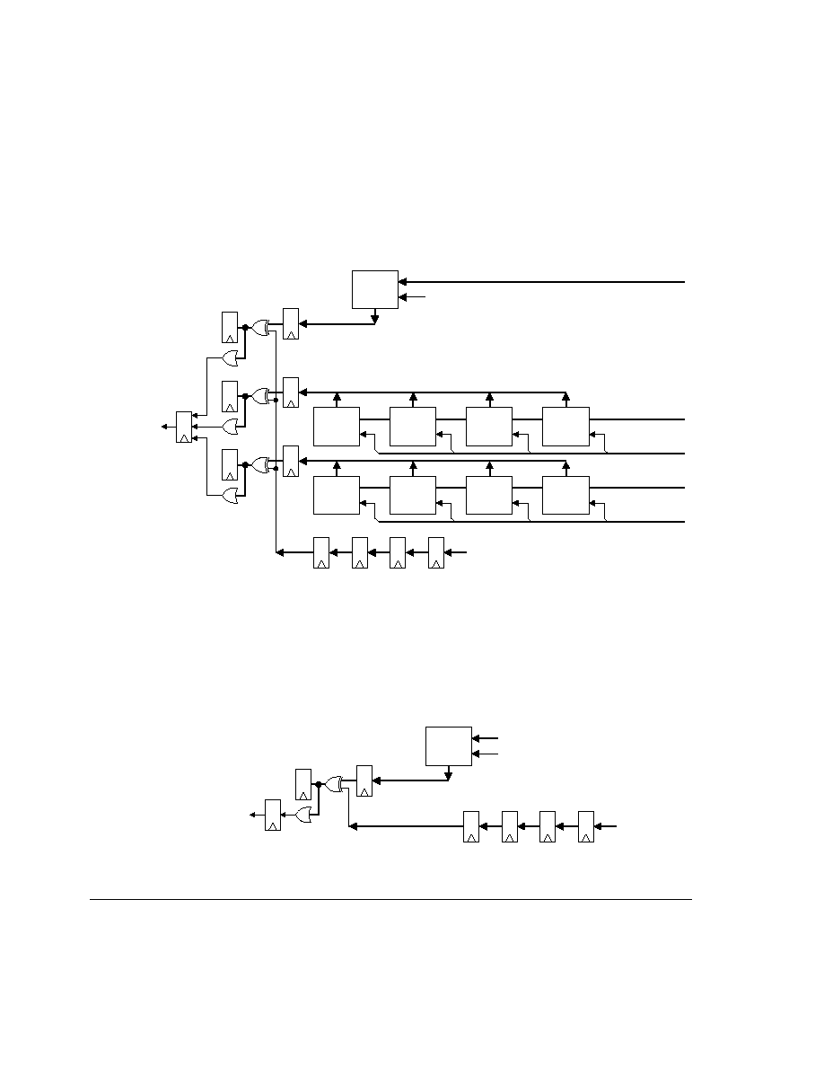
Design for Test
20-20
Copyright © 2003 ARM Limited. All rights reserved.
ARM DDI 0244C
Instruction-side MBIST arrays
The instruction-side arrays are similar to the data-side arrays, except that they do not
have a dirty array and contain only a virtual tag array. See Figure 20-16.
Figure 20-16 Instruction RAM MBIST arrays
MMU MBIST array
The MMU MBIST array is a 128-entry by 112-bit (64 bit RAM, 48 bit tag) array. Other
microTLB arrays within the MMU are created from scanable registers and are not
subject to MBIST testing. See Figure 20-17.
Figure 20-17 MMU RAM MBIST array
[0]
[1]
[2]
[3]
DATA0
Addr[7:0]
Tag CS[3:0]
Addr[10:0]
[0]
[1]
[2]
Data CS[3:0]
[3]
Addr[11:0]
DATA1
DATA2
TAG2
TAG3
TAG0
TAG1
Valid CS
DATA3
Valid
24
24
64
22
InstrData[3:0]
{16{BistData4[3:0]}}
Fail
Data log and
bitmap support
registers
Addr[4:0]
MMU CS
MMU
112
112
{28{BistData4[3:0]}}
Fail
Data log and
bitmap support
register
InstrData[3:0]

Design for Test
ARM DDI 0244C
Copyright © 2003 ARM Limited. All rights reserved.
20-21
TCM MBIST array
The TCM array does not have architecturally defined chip-select values and any such
chip select created in implementation is assigned to upper address bits and gated with
the master TCM chip select, MTESTCE2[9:8], for that array. See Figure 20-18.
Figure 20-18 TCM MBIST array
[?]
[?]
[?]
[?]
DTCM?
ITCMCS[?:0]
Addr[17:0]
[?]
[?]
[?
DTCMCS[?:0]
[?]
Addr[17:0]
DTCM?
DTCM?
ITCM?
ITCM?
ITCM?
ITCM?
DTCM?
64
64
InstrData[3:0]
{16{BistData4[3:0]}}
Fail
Data log and
bitmap support
registers

Design for Test
20-22
Copyright © 2003 ARM Limited. All rights reserved.
ARM DDI 0244C
Memory test times
Memory test times using the ARM MBIST are estimated below for minimum and
maximum cache sizes. The 30N go/nogo pattern is the benchmark for this test time
analysis. The analysis is based on the assumption that a passing part completes the
entire test. Variations in test time can exist depending on the test flow chosen for each
array. Arrays are tested in parallel according to their chip-select partitioning as defined
in Table 20-10. Typical cache sizes are assumed to be 32KB. Maximum size is 128KB
(ICache and DCache) with a 1MB TCM.
Note
In Table 20-10, address depths are in thousands of MBIST-addressable elements. A
128KB DCache has eight bytes tested in parallel. In MBIST addressing, this array has
128KB/8B or 16K addressable elements.
Table 20-10 Memory test interface cycle counts
Memory
Address depth
Number of cycles
MBIST bus width
Typical
Maximum
Typical
Maximum
ICache RAM
64 bits
4KB
16KB
123 kcycles
492 kcycles
ICache tag RAM
22 bits
2KB
2KB
62 kcycles
ICache valid RAM
24 bits
256B
256B
7.5 kcycles
DCache RAM
64 bits
4KB
16KB
123 kcycles
492 kcycles
DCache tag RAM
54 bits
2KB
2KB
62 kcycles
DCache valid RAM
24 bits
256B
256B
7.5 kcycles
DCache dirty RAM
22 bits
1KB
1KB
31 kcycles
MMU
112 bits
128B
128B
3.8 kcycles
Instruction TCM
64 bits
32KB
128KB
984 kcycles
3.9 Mcycles
Data TCM
64 bits
32KB
128KB
984 kcycles
3.9 Mcycles
Total cycles for largest memory test on interface
984 kcycles
3.9 Mcycles
Estimated test time for 200MHz cycle rate (number of cycles times 5ns)
4.9ms
19.7ms
Estimated test time without TCM RAM
0.6ms
2.5ms
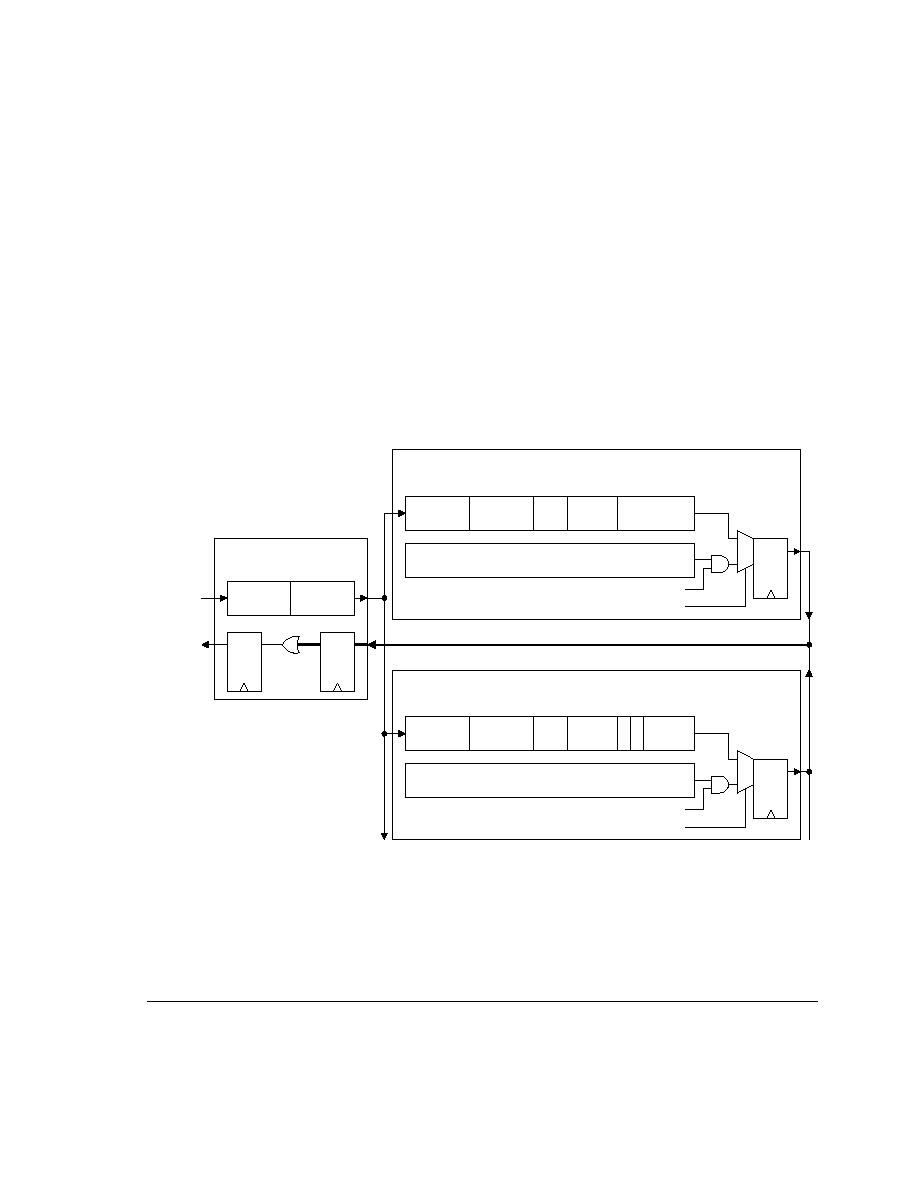
Design for Test
ARM DDI 0244C
Copyright © 2003 ARM Limited. All rights reserved.
20-23
This test time estimate does not include usual delays required for data retention or I
DDQ
tests or reset vectors at the beginning of tests.
20.3.4
MBIST Instruction Register
Figure 20-19 is an example diagram that shows the organization of the instruction shift
register in the controller and the dispatch unit. Only RAMs with a minimum of eight
addresses can be tested.
The MBIST controller is external to the memory wrapper and does not interact with the
ARM1026EJ-S processor. The processor must be held in reset during execution of
MBIST tests.
Figure 20-19 MBIST Instruction Register
Each dispatch unit connects to one or more arrays. Each array can be in more than one
physical RAM. Unused enable bits in a dispatch unit are masked. Upon completion of
the current instruction, the array enables field of the instruction is replaced with a
pass/fail flag. If the array fails, the bit is set.
Fail data
DispatchSelect
FailSelect
MEM dispatch unit
TCM dispatch unit
Fail data
DispatchSelect
FailSelect
Pattern
Control
10
5 4
0
MBIST controller
Q D
Q D
27
24 23
20 1916 15
8 7
0
MaxXaddr MaxYaddr Data
word Masked
Enables
Flags
15
9
7
0
10
8
Masked E
F
Masked
E
F
MaxXaddr MaxYaddr Data
word
27
24 23
20 1916
D Q
0
1
D Q
0
1

Design for Test
20-24
Copyright © 2003 ARM Limited. All rights reserved.
ARM DDI 0244C
To retrieve fail data, scan in a Read Dispatch Unit instruction. The next instruction shift
then shifts out the fail data. Table 20-11 shows how the fail data is formatted.
Table 20-11 Scanout formats of fail data
Fail data
Scanout format
ICache/DCache data RAM fail shiftout format:
MBISTDIN
CS[3:0] Data[3:0] index[11:0] dataXOR[63:0] MBISTDOUT[0]
ICache/DCache tag array fail shiftout:
MBISTDIN
CS[3:0] expectData[3:0] index[10:0] dataXOR[21:0] MBISTDOUT[0]
ICache/DCache valid array fail shiftout:
MBISTDIN
expectData[3:0] index[7:0] dataXOR[23:0] MBISTDOUT[0]
DCache dirty array fail shiftout:
MBISTDIN
expectData[3:0] index[9:0] dataXOR[7:0] MBISTDOUT[0]
MMU array fail shiftout:
MBISTDIN
expectData[3:0] index[4:0] dataXOR[112:0] MBISTDOUT[0]
ITCM/DTCM array fail shiftout:
MBISTDIN
expectData[3:0] index[16:0] dataXOR[63:0] MBISTDOUT[0]

Design for Test
ARM DDI 0244C
Copyright © 2003 ARM Limited. All rights reserved.
20-25
Table 20-12 lists the MBIST array enables.
20.3.5
MBIST test waveforms
Figure 20-20 shows the MBIST test start waveforms.
Figure 20-20 MBIST test start waveforms
Table 20-12 Array enables
Dispatch
instruction
bit
Array
Dispatch unit
0
ICache RAM
MEM
1
ICache tag
MEM
2
ICache valid
MEM
3
DCache RAM
MEM
4
DCache tag
MEM
5
DCache valid
MEM
6
DCache dirty
MEM
7
MMU
MEM
8
ITCM
TCMMEM
9
DTCM
TCMMEM
MBISTDOUT[0]
MBISTDIN
MBISTRUN
MBISTSHIFT
CLK
i
0
[0]
i
0
[38]
i
0
[39]
i
-1
[0]
i
-1
[38]
i
-1
[39]

Design for Test
20-26
Copyright © 2003 ARM Limited. All rights reserved.
ARM DDI 0244C
Figure 20-21 shows the MBIST test end waveforms.
Figure 20-21 MBIST test end waveforms
20.3.6
Test restrictions with the ARM BIST
Because the memory test interfaces have embedded test requirements such as
handshaking during bitmapping, there are rules regarding array enabling:
∑
Bitmap mode can only have one array enabled (InstrReg[15:0] is one-hot) for
analysis.
∑
During normal production test, any or all of the InstrReg[15:0] bits can be enabled
at a time.
∑
During normal production test, the TCM arrays and ICache and DCache arrays
can be tested simultaneously (multiple dispatch units can be active) if power
concerns can be eliminated.
∑
The maximum X,Y address must be set for the largest array enabled for that test.
In a parallel test, the dispatch unit disables array chip selects for out-of-bounds
address ranges. You can always set the maximum address, but this unnecessarily
increases test time.
Hard cores have vector sets that test the arrays in addition to soft core stimulus scripts.
Soft cores have simple verilog tasks and monitors to enable vector captures for their
implementation. Vector sets cannot be provided for soft cores because memory sizes
and configurations are not known in advance. Bitmap datalog vectors are provided for
both soft and hard cores as described in Datalog and bitmapping features on
page 20-27.
MBISTDOUT[1]
MBISTDOUT[2]
MBISTRUN
MBISTSHIFT
CLK
MBISTDOUT[0]
i
0
[0]
i
0
[1]
i
0
[2]

Design for Test
ARM DDI 0244C
Copyright © 2003 ARM Limited. All rights reserved.
20-27
20.3.7
Datalog and bitmapping features
The MBIST tests create a datalog when the first failure occurs. After completion of test,
the datalog can be shifted out by selecting the appropriate array in the instruction
register and performing a dispatch unit data shift through the MTESTDOUT[0] port.
When bitmap mode is set during MBIST test, the dispatch unit stalls the MBIST
controller whenever a read operation is received. The read operation continues until
pass/fail status is known. If the read operation passes, the MBIST controller is released
for the next operation. Failure sets the external fail flag, MBISTDOUT[2]. The
controller and dispatch unit remain stalled until the datalog is scanned out by the
external tester. The tester must branch to the bitmap datalog vector set when a fail is
observed.
The bitmap vector set asserts MBISTDSHIFT to enable shifting out the failure datalog.
MBISTDSHIFT must also clock-divide the MBISTCLKEN signal to insure that shift
timings can be met in the case of high-speed test and slow package pins.
Release of MBISTDSHIFT resets the datalog registers and releases the MBIST
controller for the next operation.
DataXOR contains only the failing bits. Failing expect data is then determined by
matching the dataXOR to an expanded {?{expectData[3:0] }}.
ArrayCS is not a duplication of the InstrReg[15:0] field as some CS fields are tied to the
Yaddr address space. This datalogged architectural ArrayCS is the same CS delivered
to the arrays in functional mode.

Design for Test
20-28
Copyright © 2003 ARM Limited. All rights reserved.
ARM DDI 0244C
20.3.8
Using non-ARM MBIST testing
If you do not require ARM MBIST, you can exclude it by using the NOMBIST compile
option. The following must be considered when disabling the ARM MBIST:
∑
Test coverage numbers proven in ARM implementations cannot be guaranteed
with non-ARM testing.
∑
Observe and control flip-flops in the memory wrapper help to reduce coverage
concerns.
∑
The ARM MBIST provides array-preservation features with the SE pin in the
memory wrapper.
Note
You must ensure I
DDQ
state preservation and preserve state during ATPG
load/unload.
∑
ORing ARM1026EJ-S and MBIST control lines into the arrays results in the
minimum timing impact. This is currently performed in the memory wrapper. The
ARM1026EJ-S processor must be held in reset during ARM MBIST testing.
∑
Validation of custom implementation is the responsibility of the user.
∑
Accessing functional data ports for writes and reads can have adverse affects on
area/performance if a hardened design differs from ARM internal
implementation.

Design for Test
ARM DDI 0244C
Copyright © 2003 ARM Limited. All rights reserved.
20-29
20.3.9
MBIST address scramble
The address scrambler enables reconfiguring address pins to match the physical
implementation of memory. The a10mBistAddrScrmbl.v and a10mTCMAddrScrmbl.v
blocks must be replaced whenever cache sizes and physical mappings change.
Changing cache size requires changing the out-of-bounds settings. Using different
cache arrays also requires changing the physical mappings to maximize leverage of
bitcell stress tests. Failure to physically map new arrays does not result in failing tests
but can result in lower screening quality.
When creating different implementations, this block must be corrected and validated to
test all arrays for each architectural chip select.
Example address scramble RTL
The RTL in Example 20-1 is an example implementation of address scrambling within
the memory wrapper:
Example 20-1 Address scrambling example
// this example assumes a 256 row array , 8 columns, 2 planes and 4 ways
// Yaddr[3:0], Xaddr[7:0] and Yaddr[6:5] as CS
wire
OutsideIRam;
assign OutsideIRAM = (|Yaddr[11:6]) | (|Xaddr[10:8]); // out of bounds address
// must mask the CS
// ArrayCS[0] translates to InstrReg[24]
assign IRamCS[3] = ArrayCS[0] & ~OutsideIRam & Yaddr[5] & Yaddr[4];
assign IRamCS[2] = ArrayCS[0] & ~OutsideIRam & Yaddr[5] & ~Yaddr[4];
assign IRamCS[1] = ArrayCS[0] & ~OutsideIRam & ~Yaddr[5] & Yaddr[4];
assign IRamCS[0] = ArrayCS[0] & ~OutsideIRam & ~Yaddr[5] & ~Yaddr[4];
assign IRamLA[11:0] = {Xaddr[7:0],Yaddr[3:0]}; // example where lowest LA
// bits select columns

Design for Test
20-30
Copyright © 2003 ARM Limited. All rights reserved.
ARM DDI 0244C
Example address scramble/mapping RTL
Example 20-2 is based on arrays with different physical organizations. This requires
simple logic that does an address scramble as a function of each array. No such logic is
required if the attached memories have similar organizations.
Example 20-2 Scrambling/mapping example
// TCM Example:
// CURRENT SCRAMBLE ASSUMPTIONS:
// 1) Ram COMPILER
// 2) 8 column mux selection
// 3) logical address assignment {rows,columns}
// 4) compiled 8-column address mapping is 0, 1, 3, 2, 4, 5, 7, 6
// col_addr[2:0] values are 000, 001, 011, 010, 100, 101, 111, 110
//
// Linear map of left to right accomplished by assigning Y[1] = Yaddr[1] and
// Y[0] = Yaddr[1] ^ Yaddr[0]
// 5) Hidden blackboxed RAMs from xxxx compiler do not exceed 256 columns. All
// row-space beyond Xaddr[7] is mapped to the Y-space to promote bitline stress
// test effectiveness
wire [11:0]
YaddrScrmbl;
assign
YaddrScrmbl[11:1] = Yaddr[11:1];
assign
YaddrScrmbl[0] = Yaddr[1] ^ Yaddr[0];
// I-side TCM
wire
OutsideITcm;
assign
OutsideITcm = (|YaddrScrmbl[11:9]) | (|Xaddr[10:8]);
// ArrayCS[0] translates to InstrReg[24]
assign
ITcmCS = ArrayCS[0] & ~OutsideITcm;
assign
ITcmLA[16:0] = {YaddrScrmbl[8:3],Xaddr[7:0],YaddrScrmbl[2:0]};
// D-side TCM
wire
OutsideDTcm;
assign
OutsideDTcm = (|YaddrScrmbl[11:9]) | (|Xaddr[10:8]);
// ArrayCS[0] translates to InstrReg[24]
assign
DTcmCS = ArrayCS[1] & ~OutsideDTcm;
assign
DTcmLA[16:0] = {YaddrScrmbl[8:3],Xaddr[7:0],YaddrScrmbl[2:0]};

ARM DDI 0244C
Copyright © 2003 ARM Limited. All rights reserved.
21-1
Chapter 21
Instruction Cycle Count
This chapter gives the instruction cycle counts and examples of interlock timing. This
chapter contains the following sections:
∑
Cycle timing considerations on page 21-2
∑
Instruction cycle counts on page 21-3
∑
Interlocks on page 21-22.

Instruction Cycle Count
21-2
Copyright © 2003 ARM Limited. All rights reserved.
ARM DDI 0244C
21.1
Cycle timing considerations
Complex instruction dependencies make it impossible to describe briefly the exact
behavior of all instructions in all circumstances. The tables in this chapter are accurate
in most cases but must never be used instead of running code on a cycle-accurate model
of the ARM1026EJ-S processor.
The performance-enhancing branch prediction architectural feature makes it
particularly difficult to count the number of cycles an instruction takes. With branch
prediction enabled, it is impossible to look at a branch in isolation and tell how many
cycles it takes. The cycle count depends on where the branch is in the pipeline and what
the processor was doing beforehand.
If instruction accesses are hitting in the ICache, then the prefetch buffer is likely to be
full. This means the prefetch unit has plenty of time to predict branches and fetch from
their targets. In this case, correctly predicted branches appear to take no cycles at all.
They are folded.
If the prefetch unit was recently flushed, or is fetching from external memory, its buffer
can be empty or only partially full. In these cases, the branch predictor does not always
have time to completely remove a branch, and it can take one or more cycles before the
following instruction is issued. This is described in more detail in Branch instructions
on page 21-8.

Instruction Cycle Count
ARM DDI 0244C
Copyright © 2003 ARM Limited. All rights reserved.
21-3
21.2
Instruction cycle counts
Unless stated otherwise, cycle counts and result latencies described here are best case
numbers. They assume:
∑
no outstanding data dependencies between an instruction and a previous
instruction
∑
the instruction does not encounter any resource conflicts
∑
all data accesses hit in the DCache and do not cross protection region boundaries
∑
all instruction accesses hit in the ICache.
The tables in this section show the number of cycles an instruction takes to execute and
the number of cycles after which the result of the instruction is available to a following
instruction. These numbers differ because after an instruction has left the Execute stage
of the pipeline, a second instruction can start to execute, even when the first instruction
has not produced its final result. This is only the case when the second instruction is not
dependent on the result from the first.
Instructions that change the PC cause the pipeline to be flushed and restarted with a
fetch of a new instruction. By the time the new instruction executes, it is likely that any
dependencies on previous instructions have been cleared.
Three figures are typically given for each instruction:
Condition pass cycles
This is the number of cycles taken if the instruction passes its condition
code check, that is, the number of cycles between this instruction starting
to execute and the next instruction starting to execute. This is usually the
same as the number of iterations the instruction makes in the Execute
stage of the ALU pipeline, or the number of iterations a load or store
multiple instruction makes in the Execute stage of the LSU pipeline.
If an instruction changes the instruction stream, then the condition pass
cycles indicates the number of cycles before the new PC is available plus
the number of cycles it takes to refill the pipe to the point where a new
instruction enters Execute in the next cycle.
Condition fail cycles
This is the number of cycles taken if the instruction fails its condition
code check, that is, the number of cycles between this instruction entering
the Execute stage of the pipeline and failing its condition code check and
the next instruction entering the Execute stage.

Instruction Cycle Count
21-4
Copyright © 2003 ARM Limited. All rights reserved.
ARM DDI 0244C
Result cycles
This is the number of cycles it takes for the instruction to produce its
result. It is the number of cycles that must be taken up by the current
instruction and following independent instructions before a dependent
instruction can be run without interlocking. It can be larger than condition
pass cycles in cases where an instruction produces a result later than the
Execute stage of the pipeline.
If condition pass cycles is greater than result cycles for an instruction,
then the result is always available to a following instruction.
See Interlocks on page 21-22 for details of result forwarding paths and the pipeline
stages in which instructions have to read registers.
Instructions that change mode by writing the control section of the CPSR are
highlighted in some of the tables because they have to wait for the LSU pipe to empty.
This is noted in the tables because it makes a significant difference to the execution time
if there are any outstanding load misses. Exceptions also change mode, causing a delay
while the LSU pipe empties.
The instructions are described in the following sections:
∑
Data processing instructions on page 21-5
∑
Multiply instructions on page 21-7
∑
Branch instructions on page 21-8
∑
MRS and MSR instructions on page 21-9
∑
SWI instruction on page 21-9
∑
Load and store instructions on page 21-9
∑
Load multiple and store multiple instructions on page 21-14
∑
Preload instructions on page 21-15
∑
Coprocessor instructions on page 21-15
∑
Semaphore instructions on page 21-16
∑
Thumb data processing instructions on page 21-17
∑
Thumb multiply instructions on page 21-19
∑
Thumb branch instructions on page 21-19
∑
Thumb load instructions and store instructions on page 21-20
∑
Thumb load multiple and store multiple instructions on page 21-21.

Instruction Cycle Count
ARM DDI 0244C
Copyright © 2003 ARM Limited. All rights reserved.
21-5
21.2.1
Data processing instructions
The simple data processing instructions are:
AND, EOR, SUB, RSB, ADD,
ADC, SBC, RSC,CMN, ORR,
ORR, MOV, BIC, MVN, TST,
TEQ, CMP, QADD, QDADD, QSUB, QDSUB, CLZ
Table 21-1 shows the addressing mode 1 subcategories of data processing instructions.
Table 21-2 shows examples of data processing cycle counts. In the table, any of the
simple data processing operations can be substituted for AND.
Table 21-1 Subcategories of data processing instructions
Subcategory
Format
Example
Immediate
OP Rd, Rn, #imm
ADD R1, R2, #1
Register
OP Rd, Rn, Rm
AND R1, R2, R3
Immediate shifted register
OP Rd, Rn, Rm LSL #imm
AND R1, R2, R3 LSL #1
Register shifted register
OP Rd, Rn, Rm LSL Rs
AND R1, R2, R3 LSL R4
Table 21-2 Cycle counts of data processing instructions
Example instruction
Notes
Change
mode
Pass
Fail
Result
available
AND Rd, Rn, #imm
-
No
1
1
1
AND Rd, Rn, Rm
-
No
1
1
1
AND Rd, Rn, Rm LSL #imm
-
No
1
1
1
AND Rd, Rn, Rm LSL Rs
-
No
2
2
2
ANDS Rd, Rn, #imm
Set flags
No
1
1
1
ANDS Rd, Rn, Rm
Set flags
No
1
1
1
ANDS Rd, Rn, Rm LSL #imm
Set flags
No
1
1
1
ANDS Rd, Rn, Rm LSL Rs
Set flags
No
2
2
2

Instruction Cycle Count
21-6
Copyright © 2003 ARM Limited. All rights reserved.
ARM DDI 0244C
Most data processing instructions take one cycle to execute, after which their result is
available for use. The exceptions are instructions that involve register-controlled shifts,
saturating instructions, and instructions that write to the PC.
A simple MOV from a register, with no shift that writes the PC requires four extra
cycles to refill the pipeline. More complex operations that write to the PC take five extra
cycles to refill the pipeline.
AND PC, Rn, #imm
To PC
No
1 + 5
1
N/A
AND PC, Rn, Rm
To PC
No
1 + 5
1
N/A
AND PC, Rn, Rm LSL #imm
To PC
No
1 + 5
1
N/A
AND PC, Rn, Rm LSL Rs
To PC
No
2 + 5
2
N/A
ANDS PC, Rn, #imm
To PC, restore CPSR
Yes
2 + 5
1
N/A
ANDS PC, Rn, Rm
To PC, restore CPSR
Yes
2 + 5
1
N/A
ANDS PC, Rn, Rm LSL #imm
To PC, restore CPSR
Yes
2 + 5
1
N/A
ANDS PC, Rn, Rm LSL Rs
To PC, restore CPSR
Yes
2 + 5
2
N/A
MOV PC, Rn
Zero shift MOV to PC
No
1 + 4
1
N/A
CLZ Rd, Rm
-
No
1
1
1
QADD Rd, Rm, Rn
Sets Q flag
No
1
1
2
QSUB Rd, Rm, Rn
Sets Q flag
No
1
1
2
QDADD Rd, Rm, Rn
Sets Q flag
No
1
1
2
QDSUB Rd, Rm, Rn
Sets Q flag
No
1
1
2
Table 21-2 Cycle counts of data processing instructions (continued)
Example instruction
Notes
Change
mode
Pass
Fail
Result
available

Instruction Cycle Count
ARM DDI 0244C
Copyright © 2003 ARM Limited. All rights reserved.
21-7
21.2.2
Multiply instructions
Table 21-3 shows the cycle counts of multiply instructions. For long multiplies, the least
significant word of the result is always the first available. The most significant word is
available in the following cycle. This is why there are two cycle counts for instructions
whose results extend over one word.
If the number of pass cycles is greater than the number of result cycles, then the result
cycles dominate. Multiplies that set the flags other than Q have to sit in Execute stage
for several cycles, because the the ALU must calculate the new flags. Sometimes it
might be possible to use a multiply that does not set the flags, followed by a compare
of the result that does set the flags. This is appropriate where a useful instruction can be
inserted between the multiply and the compare.
Table 21-3 Cycle counts of multiply instructions
Instruction
Notes
Pass Fail
Rd
(Lo/Hi) Flags
SMUL<x><y> Rd, Rm, Rs
16
◊ 16 -> 32
1
1
2
-
SMLA<x><y> Rd, Rm, Rs, Rn
16
◊ 16 + 32 -> 32
2
2
2
-
SMLAL<x><y> RdLo, RdHi, Rm, Rs
16
◊ 16 + 64 -> 64
2
2
2/3
-
SMULW<x> Rd, Rm, Rs
32
◊ 16 -> 32, upper 32 bits
1
1
2
-
SMLAW<x> Rd, Rm, Rs, Rn
32
◊ 16 + 32 -> 32, upper 32 bits
2
2
2
-
MUL Rd, Rm, Rs
32
◊ 32 -> 32
2
2
3
-
MULS Rd, Rm, Rs
32
◊ 32 -> 32, set flags
4
2
3
4
MLA Rd, Rm, Rs, Rn
32
◊ 32 + 32 -> 32
2
2
3
-
MLAS Rd, Rm, Rs, Rn
32
◊ 32 + 32 -> 32, set flags
4
2
3
4
UMULL RdLo, RdHi, Rm,Rs
32
◊ 32 -> 64, unsigned
3
2
3/4
-
UMULLS RdLo, RdHi, Rm, Rs
32
◊ 32 -> 64, unsigned, set flags
5
2
3/4
5
UMLAL RdLo, RdHi, Rm, Rs
32
◊ 32 + 64 -> 64, unsigned
3
2
3/4
-
UMLALS RdLo, RdHi, Rm, Rs
32
◊ 32 + 64 -> 64, unsigned, set flags
5
2
3/4
5
SMULL RdLo, RdHi, Rm,Rs
32
◊ 32 -> 64, signed
3
2
3/4
-
SMULLS RdLo, RdHi, Rm,Rs
32
◊ 32 -> 64, signed, set flags
5
2
3/4
5
SMLAL RdLo, RdHi, Rm, Rs
32
◊ 32 + 64 -> 64, signed
3
2
3/4
-
SMLALS RdLo, RdHi, Rm, Rs
32
◊ 32 + 64 -> 64, signed, set flags
5
2
3/4
5

Instruction Cycle Count
21-8
Copyright © 2003 ARM Limited. All rights reserved.
ARM DDI 0244C
21.2.3
Branch instructions
This section describes the following instructions:
B, BL, BX, BLX, BXJ.
When branch prediction is enabled, unconditional and conditional backward branches
are predicted taken, and conditional forward branches are predicted not taken. See
Branch instruction cycle summary on page 5-6 for more detail.
Table 21-4 Cycle counts of branch instructions
Unpredicted
Predicted
Instruction
Pass
Fail
Predictable
Correctly Incorrectly
B <address>
5
1
Yes
0 to 3
a
a. Assuming all accesses hit in the ICache. When the prefetch unit has had time
to fold a branch it appears to take zero cycles. When the prefetch unit has been
recently been flushed and is empty, it takes three cycles to obtain the
instruction at the branch target.
5
BL <address>
5
2
Yes
1 to 3
-
BX Rm
5
2
No
-
-
BLX Rm
5
2
No
-
-
BLX <Imm24>
5
N/A
Yes
1 to 3
-
BXJ Rm
5
2
No
-
-

Instruction Cycle Count
ARM DDI 0244C
Copyright © 2003 ARM Limited. All rights reserved.
21-9
21.2.4
MRS and MSR instructions
MSR instructions that write just the flags run quickly. MSRs that change mode take
more cycles and have to wait for the LSU pipeline to be empty before they start to
execute. Table 21-5 shows the cycle counts for MRS and MSR instructions.
21.2.5
SWI instruction
A SWI instruction takes five cycles to execute, or two cycles if it fails its condition code
check. This is true for the ARM and Thumb SWI instructions.
21.2.6
Load and store instructions
This section describes the following instructions:
LDR, LDRD, LDRB, LDRBT, LDRH, LDRSB, LDRSH, LDRT,
STM, STR, STRD, STRB, STRBT, STRH, STRT.
Loads and stores all take one cycle to execute unless they use a scaled register offset or
scaled register pre-indexed addressing mode, in which case they take three cycles.
Load and stores with a scaled register offset or pre-indexed addressing mode and a base
plus offset with an LSL of 0 or 2, or a base minus offset with an LSL of 0 are optimized
to execute in one cycle.
Loads to the PC take seven cycles to execute unless they use a scaled register offset or
pre-indexed addressing mode, in which case they take nine cycles.
Table 21-5 Cycle counts of MRS and MSR instructions
Example instruction
Notes
Change mode
Pass
Fail
MRS Rd, CPSR
-
No
1
1
MRS Rd, SPSR
-
No
1
1
MSR_f CPSR, Rn
Only flags
No
1
1
MSR_f CPSR, #<cns>
Only flags
No
1
1
MSR CPSR, Rn
Not only flags
Yes
5
1
MSR CPSR, #<cns>
Not only flags
Yes
5
1
MSR SPSR, Rn
-
No
4
2
MSR SPSR, #<cns>
-
No
4
2

Instruction Cycle Count
21-10
Copyright © 2003 ARM Limited. All rights reserved.
ARM DDI 0244C
For all loads, the loaded data is available for use one cycle after the last Execute stage
of the load.
The base write-back value is calculated in the ALU pipeline Execute stage and is
usually available immediately for forwarding to the Decode stage of the following
instruction. For scaled register pre-indexed addressing mode, the base write-back is
available in the third Execute stage for forwarding to the next instruction.
Table 21-6 shows the cycle counts of the load instructions.
Table 21-6 Cycle counts of load instructions
Example instruction
Pass
Fail
Base write-back
Load data
LDR PC, [Rn], #<cns>
7
2
1
-
LDR PC, [Rn, #<cns>]
7
2
-
-
LDR PC, [Rn, #<cns>]!
7
2
1
-
LDR PC, [Rn], Rm, <shf><cns>
7
2
3
-
LDR PC, [Rn, Rm]
7
2
-
-
LDR PC, [Rn, Rm]!
7
2
1
-
LDR PC, [Rn, Rm, <shf><cns>]
9
2
-
-
LDR PC, [Rn, Rm, <shf><cns>]!
9
2
3
-
LDR Rd, [Rn], #<cns>
1
1
1
2
LDRT Rd, [Rn], #<cns>
1
1
1
2
LDRB Rd, [Rn], #<cns>
1
1
1
2
LDRBT Rd, [Rn], #<cns>
1
1
1
2
LDR Rd, [Rn, #<cns>]
1
1
-
2
LDR Rd, [Rn, #<cns>]!
1
1
1
2
LDRB Rd, [Rn, #<cns>]
1
1
-
2
LDRB Rd, [Rn, #<cns>]!
1
1
1
2
LDR Rd, [Rn], Rm, <shf><cns>
1
1
1
2
LDRT Rd, [Rn], Rm, <shf><cns>
1
1
1
2
LDRB Rd, [Rn], Rm, <shf><cns>
1
1
1
2

Instruction Cycle Count
ARM DDI 0244C
Copyright © 2003 ARM Limited. All rights reserved.
21-11
LDRBT Rd, [Rn], Rm, <shf><cns>
1
1
1
2
LDR Rd, [Rn,Rm]
1
1
-
2
LDR Rd, [Rn,Rm]!
1
1
1
2
LDRB Rd, [Rn, Rm]
1
1
-
2
LDRB Rd, [Rn, Rm]!
1
1
1
2
LDR Rd, [Rn, Rm, <shf><cns>]
3
2
-
4
LDR Rd, [Rn, Rm, <shf><cns>]!
3
2
3
4
LDRB Rd, [Rn, Rm, <shf><cns>]
3
2
-
4
LDRB Rd, [Rn, Rm, <shf><cns>]!
3
2
3
4
LDRSB Rd, [Rn], Rm
1
1
1
2
LDRSB Rd, [Rn], #<cns>
1
1
1
2
LDRSB Rd, [Rn, Rm]
1
1
-
2
LDRSB Rd, [Rn, Rm]!
1
1
1
2
LDRSB Rd, [Rn, #<cns>]
1
1
-
2
LDRSB Rd, [Rn, #<cns>]!
1
1
1
2
LDRH Rd, [Rn], Rm
1
1
1
2
LDRH Rd, [Rn], #<cns>
1
1
1
2
LDRH Rd, [Rn, Rm]
1
1
-
2
LDRH Rd, [Rn, Rm]!
1
1
1
2
LDRH Rd, [Rn, #<cnt>]
1
1
-
2
LDRH Rd, [Rn, #<cnt>]!
1
1
1
2
LDRSH Rd, [Rn], Rm
1
1
1
2
LDRSH Rd, [Rn], #<cns>
1
1
1
2
LDRSH Rd, [Rn, Rm]
1
1
-
2
LDRSH Rd, [Rn, Rm]!
1
1
1
2
Table 21-6 Cycle counts of load instructions (continued)
Example instruction
Pass
Fail
Base write-back
Load data

Instruction Cycle Count
21-12
Copyright © 2003 ARM Limited. All rights reserved.
ARM DDI 0244C
Table 21-7 shows the cycle counts of the store instructions.
LDRSH Rd, [Rn, #<cns>]
1
1
-
2
LDRSH Rd, [Rn, #<cns>]!
1
1
1
2
LDRD Rd, [Rn], Rm
1
1
1
2
LDRD Rd, [Rn], #<cns>
1
1
1
2
LDRD Rd, [Rn, Rm]
1
1
-
2
LDRD Rd, [Rn, Rm]!
1
1
1
2
LDRD Rd, [Rn, #<cns>]
1
1
-
2
LDRD Rd, [Rn, #<cns>]!
1
1
1
2
Table 21-7 Cycle counts of store instructions
Example instruction
Pass
Fail
Base write-back
STR Rd, [Rn], #<cns>
1
1
1
STRT Rd, [Rn], #<cns>
1
1
1
STRB Rd, [Rn], #<cns>
1
1
1
STRBT Rd, [Rn], #<cns>
1
1
1
STR Rd, [Rn, #<cns>]
1
1
-
STR Rd, [Rn, #<cns>]!
1
1
1
STRB Rd, [Rn, #<cns>]
1
1
-
STRB Rd, [Rn, #<cns>]!
1
1
1
STR Rd, [Rn], Rm, <shf><cns>
1
1
1
STRT Rd, [Rn], Rm, <shf><cns>
1
1
1
STRB Rd, [Rn], Rm, <shf><cns>
1
1
1
STRBT Rd, [Rn], Rm, <shf><cns>
1
1
1
STR Rd, [Rn, Rm]
1
1
-
Table 21-6 Cycle counts of load instructions (continued)
Example instruction
Pass
Fail
Base write-back
Load data

Instruction Cycle Count
ARM DDI 0244C
Copyright © 2003 ARM Limited. All rights reserved.
21-13
STR Rd, [Rn, Rm]!
1
1
1
STRB Rd, [Rn, Rm]
1
1
-
STRB Rd, [Rn, Rm]!
1
1
1
STR Rd, [Rn, Rm, <shf><cns>]
3
2
-
STR Rd, [Rn, Rm, <shf><cns>]!
3
2
3
STRB Rd, [Rn, Rm, <shf><cns>]
3
2
-
STRB Rd, [Rn, Rm, <shf><cns>]!
3
2
3
STRH Rd, [Rn], Rm
1
1
1
STRH Rd, [Rn], #<cns>
1
1
1
STRH Rd, [Rn, Rm]
1
1
-
STRH Rd, [Rn, Rm]!
1
1
1
STRH Rd, [Rn, #<cnt>]
1
1
-
STRH Rd, [Rn, #<cnt>]!
1
1
1
STRD Rd, [Rn], Rm
1
1
1
STRD Rd, [Rn], #<cns>
1
1
1
STRD Rd, [Rn, Rm]
1
1
-
STRD Rd, [Rn, Rm]!
1
1
1
STRD Rd, [Rn, #<cns>]
1
1
-
STRD Rd, [Rn, #<cns>]!
1
1
1
Table 21-7 Cycle counts of store instructions (continued)
Example instruction
Pass
Fail
Base write-back

Instruction Cycle Count
21-14
Copyright © 2003 ARM Limited. All rights reserved.
ARM DDI 0244C
21.2.7
Load multiple and store multiple instructions
An LDM can load two registers per cycle. If the initial access is not to a 64-bit aligned
address, an extra cycle is required because only a single register can be loaded in the
first cycle.
An LDM/STM will iterate in the LSU pipeline Execute and Memory stages until the
last register in the list has been loaded. Data processing instructions cannot run under
an LDM/STM, and are held in the ALU pipeline Execute stage. Load/store instructions
cannot run under an LDM/STM, and are held in the LSU pipeline Decode stage.
If an LDM loads the PC, it is loaded from the last access, and six more cycles are
required to refill the pipeline.
Table 21-8 shows the cycle counts of simple load/store multiple instructions. L is the
number of cycles it takes to load the part of the register list before the PC. For example,
if the list of registers is {r1, r2, PC}, L is one or two depending on whether the address
to load r1 from is aligned to 64 bits. If it is aligned, r1 and r2 are loaded in one cycle. If
not, then it takes one cycle to load r1 and a second cycle to load r2.
Table 21-8 Cycle counts of load multiple and store multiple instructions
Example instruction
Change mode
Pass
Fail
Base write-back
First load data
STM Rn, <...>
No
L
1
-
-
STM Rn!, <...>
No
L
1
1
-
STM Rn, <...>^
No
L
1
-
-
STM Rn!, <...>^
No
L
1
1
-
LDM Rn, <...noPC>
No
L
1
-
2
LDM Rn!, <...noPC>
No
L
1
1
2
LDM Rn, <...noPC>^
No
L
1
-
2
LDM Rn!, <...noPC>^
No
L
1
1
2
LDM Rn, <...PC>
No
L + 6
2
-
2
LDM Rn!, <...PC>
No
L + 6
2
1
2
LDM Rn, <...PC>^
Yes
L + 7
2
-
2
LDM Rn!, <...PC>^
Yes
L + 7
2
1
2

Instruction Cycle Count
ARM DDI 0244C
Copyright © 2003 ARM Limited. All rights reserved.
21-15
21.2.8
Preload instructions
Table 21-9 shows the cycle counts of preload instructions.
21.2.9
Coprocessor instructions
This section describes the following instructions:
CDP, LDC, MCR, MCRR, MRC, MRRC, STC.
Table 21-10 shows the cycle counts of the coprocessor instructions. The maximum
number of cycles taken by one of these instructions depends on the coprocessor
involved. Cycles shown are the minimum cycle count for a tightly coupled coprocessor
such as the VFP10 (Rev 1) coprocessor. Other coprocessors might have greater
minimum cycle count.
Table 21-9 Cycle counts of preload instructions
Instruction
Number of cycles
PLD [Rn,#-<cns>]
1
PLD [Rn, #<cns>]
1
PLD [Rn, -Rm]
1
PLD [Rn, -Rm, <shf><cns>]
3
PLD [Rn, Rm]
1
PLD [Rn, Rm, <shf><cns>]
3
Table 21-10 Cycle counts of coprocessor instructions
Example instruction
Pass
Fail
Base write-back
Data
Flags
CDP <copr>, <op1>, CRd, CRn, CRm, <op2>
1
1
-
-
-
MCR <copr>, <op1>, Rd, CRn, CRm, <op2>
1
1
-
-
-
MCRR <copr>, <op>, [Rd], [Rn], <CRm>
1
1
-
-
-
MRC <copr>, <op1>, Rd, CRn, CRm, <op2>
1
1
-
2
-
MRC <copr>, <op1>, PC, CRn, CRm, <op2>
2
2
-
2
2
MRRC <copr>, <op>, [Rd], [Rn], <CRm>
1
1
-
2
-
STC <copr>, CRd, [Rn], {option}
L
1
1
-
-

Instruction Cycle Count
21-16
Copyright © 2003 ARM Limited. All rights reserved.
ARM DDI 0244C
21.2.10 Semaphore instructions
This section describes the SWP and SWPB instructions.
A swap takes two cycles, but before it can be executed, all outstanding loads and stores
are completed. Table 21-11 shows the cycle counts of swap instructions.
STC <copr>, CRd, [Rn], #<cns>!
L
1
1
-
-
STCL <copr>, CRd, [Rn], {option}
L
1
1
-
-
STCL <copr>, CRd, [Rn], #<cns>!
L
1
1
-
-
STC <copr>, CRd, [Rn, #<cns>]
L
1
-
-
-
STC <copr>, CRd, [Rn, #<cns>]!
L
1
1
-
-
STCL <copr>, CRd, [Rn, #<cns>]
L
1
-
-
-
STCL <copr>, CRd, [Rn, #<cns>]!
L
1
1
-
-
LDC <copr>, CRd, [Rn], {option}
L
1
1
2
-
LDC <copr>, CRd, [Rn], #<cns>!
L
1
1
2
-
LDCL <copr>, CRd, [Rn], {option}
L
1
1
L + 2
-
LDCL <copr>, CRd, [Rn], #<cns>!
L
1
1
L + 2
-
LDC <copr>, CRd, [Rn, #<cns>]
L
1
-
2
-
LDC <copr>, CRd, [Rn, #<cns>]!
L
1
1
2
-
LDCL <copr>, CRd, [Rn, #<cns>]
L
1
-
L + 2
-
LDCL <copr>, CRd, [Rn, #<cns>]!
L
1
1
L + 2
-
Table 21-10 Cycle counts of coprocessor instructions (continued)
Example instruction
Pass
Fail
Base write-back
Data
Flags
Table 21-11 Cycle counts of swap instructions
Example instruction
Pass
Fail
Result available
SWP Rd, Rm, [Rn]
2
2
2
SWPB Rd, Rm, [Rn]
2
2
2

Instruction Cycle Count
ARM DDI 0244C
Copyright © 2003 ARM Limited. All rights reserved.
21-17
21.2.11 Thumb data processing instructions
Thumb data processing instructions behave in a way similar to ARM instructions.
Table 21-12 shows the cycle counts of Thumb data processing instructions.
Table 21-12 Cycle counts of Thumb data processing instructions
Example instruction
Number of cycles
Result available
LSL Rd, Rm, #sh_imm5
1
1
LSR Rd, Rm, #sh_imm5
1
1
ASR Rd, Rm, #sh_imm5
1
1
ADD Rd, Rn, Rm
1
1
SUB Rd, Rn, Rm
1
1
ADD Rd, Rn, #imm3
1
1
SUB Rd, Rn, #imm3
1
1
MOV Rd, #imm8
1
1
CMP Rd, #imm8
1
1
ADD Rd, #imm8
1
1
SUB Rd, #imm8
1
1
AND Rd, Rm
1
1
EOR Rd, Rm
1
1
LSL Rd, Rs
2
2
LSR Rd, Rs
2
2
ASR Rd, Rs
2
2
ADC Rd, Rm
1
1
SBC Rd, Rm
1
1
ROR Rd, Rs
2
2
TST Rn, Rm
1
1
NEG Rd, Rm
1
1
CMP Rd, Rm
1
1

Instruction Cycle Count
21-18
Copyright © 2003 ARM Limited. All rights reserved.
ARM DDI 0244C
CMN Rd, Rm
1
1
ORR Rd, Rm
1
1
BIC Rd, Rm
1
1
MVN Rd, Rm
1
1
ADD Rd, Hm
1
1
ADD Hd, Rm
1
1
ADD Hd, Hm
1
1
CMP Rd, Hm
1
1
CMP Hd, Rm
1
1
CMP Hd, Hm
1
1
MOV Rd, Hm
1
1
MOV Hd, Rm
1
1
MOV Hd, Hm
1
1
ADD Rd, PC, #imm
1
1
ADD Rd, SP, #imm
1
1
ADD SP, #imm
1
1
SUB SP, #imm
1
1
ADD PC, Rm
6
-
ADD PC, Hm
6
-
MOV PC, Rm
5
-
MOV PC, Hm
5
-
Table 21-12 Cycle counts of Thumb data processing instructions (continued)
Example instruction
Number of cycles
Result available

Instruction Cycle Count
ARM DDI 0244C
Copyright © 2003 ARM Limited. All rights reserved.
21-19
21.2.12 Thumb multiply instructions
The Thumb multiply instruction behaves in a way similar to the ARM MULS
instruction. Table 21-13 shows the cycle count of the Thumb multiply instruction.
21.2.13 Thumb branch instructions
Thumb BL and BLX to an immediate value are encoded as two Thumb instructions. The
first instruction is a data processing instruction that puts an immediate value into r14.
This takes three cycles. The second instruction adds an immediate value to r14 and
fetches from that address. This takes four cycles before the next instruction is in
Execute. Table 21-14 shows the cycle counts of Thumb branch instructions.
21.2.14 Thumb SWI instruction
An SWI instruction takes five cycles to execute, or two cycles if it fails its condition
code check. This is true for both the ARM and Thumb SWI instruction.
Table 21-13 Cycle count of the Thumb multiply instruction
Example instruction
Notes
Number of cycles
Result
Rd
Flags
MUL Rd, Rm
32
◊ 32 + 32 -> 32, set flags
4
3
4
Table 21-14 Cycle counts of Thumb branch instructions
Unpredicted
Predicted
Instruction
Pass Fail
Predictable
Correctly
Incorrectly
B <address>
5
N/A
Yes
0 to 3
a
a. Assuming all accesses hit in the ICache. When the prefetch unit has had time
to fold a branch it appears to take zero cycles. When the prefetch unit has been
recently flushed and is empty it takes three cycles to obtain the instruction at
the branch target (See Chapter 5 Prefetch Unit).
5
BL <address>
3 + 4
N/A
Yes
1 to 3
-
BX Rm
5
N/A
No
-
-
BLX Rm
5
N/A
No
-
-
BLX <Imm>
3 + 4
N/A
Yes
1 to 3
-

Instruction Cycle Count
21-20
Copyright © 2003 ARM Limited. All rights reserved.
ARM DDI 0244C
21.2.15 Thumb load instructions and store instructions
Thumb load/store instructions behave in a way similar to ARM load/store instructions.
Table 21-16 shows the cycle counts of Thumb load instructions.
Table 21-15 shows the cycle counts of Thumb store instructions.
Table 21-15 Cycle counts of Thumb load instructions
Example instruction
Number of cycles
Load data
LDR Rd, [Rn, Rm]
1
2
LDRB Rd, [Rn, Rm]
1
2
LDRSB Rd, [Rn, Rm]
1
2
LDRH Rd, [Rn, Rm]
1
2
LDRSH Rd, [Rn, Rm]
1
2
LDR Rd, [Rb, #imm5]
1
2
LDRB Rd, [Rb, #imm5]
1
2
LDRH Rd, [Rn, #imm5]
1
2
LDR Rd, [SP, #imm8]
1
2
Table 21-16 Cycle counts of Thumb store instruction
Example instruction
Number of cycles
STR Rd, [Rn, Rm]
1
STRB Rd, [Rn, Rm]
1
STRH Rd, [Rn, Rm]
1
STR Rd, [Rb, #imm5]
1
STRB Rd, [Rb, #imm5]
1
STRH Rd, [Rn, #imm5]
1
STR Rd, [SP, #imm8]
1

Instruction Cycle Count
ARM DDI 0244C
Copyright © 2003 ARM Limited. All rights reserved.
21-21
21.2.16 Thumb load multiple and store multiple instructions
Thumb load/store multiple instructions behave in the same way as ARM load/store
multiple instructions. Table 21-17 shows the cycle counts of Thumb load/store multiple
instructions.
L is the number of cycles it takes to load the part of the register list before the PC. For
example, for {r1, r2, PC} L is 1 or 2 depending on whether the address to load r1 from
is aligned to 64 bits. If it is aligned, r1 and r2 is loaded in one cycle. If not, then it takes
one cycle to load r1 and a second cycle to load r2.
Table 21-17 Cycle counts of Thumb load/store multiple instructions
Example instruction
Number of cycles
Base write-back
First load data
PUSH {rlist}
L
-
-
PUSH {rlist, LR}
L
-
-
STMIA Rn!, {rlist}
L
1
-
POP {rlist}
L
-
2
POP {rlist, PC}
L + 6
-
2
LDMIA Rn!, {rlist}
L
1
2

Instruction Cycle Count
21-22
Copyright © 2003 ARM Limited. All rights reserved.
ARM DDI 0244C
21.3
Interlocks
In almost all cases, the integer core uses forwarding to resolve data dependencies
between instructions. For the remaining cases, hardware-imposed interlocks (pipeline
stalls) are used to ensure the correct operation of an instruction.
One of the more common causes of data dependency interlocks are data processing
instructions that have a source register that is loaded from memory by the previous
instruction. The previous instruction might be an LDR, in which case this data is usually
available after a one-cycle interlock. The data processing instruction gets as far as
Decode before it interlocks. It interlocks in Decode because this is where it reads its
source registers.
Another common cause of data dependency interlocks is load/store instructions where
the load/store address is dependent on the result of the previous instruction. The
previous instruction might be a data processing instruction, in which case the result is
usually available after a one-cycle interlock, or it might be an LDR, in which case the
the loaded data is usually available after a two-cycle interlock. The load/store
instruction gets as far as Decode before it interlocks. It interlocks in Decode because
this is where it calculates the load/store address.
Pipeline interlocks are also used to resolve hardware dependencies in the pipeline.
Some common examples of hardware dependencies are:
∑
a data processing instruction waiting for the LSU to an finish an existing LDM or
STM
∑
a new load waiting for the LSU to finish an existing LDM or STM
∑
a new multiply waiting for a previous multiply to free up the first stage of the
multiplier.
The integer core generates most interlocks as late as possible. For instance, a multiply
accumulate instruction can start before the accumulate operands are available and stops
only when the values are required. This gives the maximum time possible for previous
instructions to generate the required data and minimizes occurrences of interlocks.
The integer core implements forwarding paths to enable almost any result to be used as
soon as it is calculated. The forwarding paths are shown in Figure 21-1 on page 21-23.

Instruction Cycle Count
ARM DDI 0244C
Copyright © 2003 ARM Limited. All rights reserved.
21-23
Figure 21-1 Pipeline forwarding paths
The register bank has four read ports:
∑
Port A
∑
Port B
∑
Port S1
∑
Port S2.
In the Decode stage, the integer unit reads port A and port B. Ports A and B are for
operands for ALU and multiply instructions and registers to generate addresses for
loads, stores, and unpredicted branches.
In the Execute stage, the LSU reads port S1 and port S2. Ports S1 and S2 are for store
data for STRs and STMs and for transfers to coprocessors.
The register bank has three write ports:
∑
Port W
∑
Port L1
∑
Port L2.
The integer unit writes to port W, and the LSU writes to port L1 and port L2 at the end
of the Write stage. Port W is for writing results from the ALU pipeline. The results
include ALU operations, multiplies, and base register write-backs for loads and stores.
Ports L1 and L2 are for writing loaded data for LDRs and LDMs and for transfers from
coprocessors.
LSU
pipeline
ALU
pipeline
Fetch
Issue
Decode
Execute
Memory
Write
Read port S1
Read port S2
Write port L1
Write port L2
Write port W
Read port A
Read port B

Instruction Cycle Count
21-24
Copyright © 2003 ARM Limited. All rights reserved.
ARM DDI 0244C
21.3.1
Examples of interlocking and forwarding
Example 21-1 through Example 21-13 on page 21-27 illustrate interlocking and
forwarding.
Example 21-1 is the simplest case of forwarding. The ADD is dependent on the MOV
as the MOV writes r0 and the ADD reads it. The write of 1 into register r0 does not
happen until the end of the Write stage of the pipeline, but the correct value for r0, a 1,
is forwarded to the ADD in the ADD Decode stage by the ALU pipeline
Execute-to-Decode forwarding path. This enables the ADD to run with no interlocks.
Example 21-1
MOV R0, #1
ADD R1, R0, #1
In Example 21-2, the ADD is dependent on the MOV, and there is a single-cycle SUB
between them. The write of 1 to r0 has not happened when the ADD is reading its source
registers because the MOV is in the Memory stage when the ADD is in the Decode
stage. The correct value for r0, a 1, is forwarded to the ADD Decode stage by the ALU
pipeline Memory-to-Decode forwarding path. This enables the ADD to run with no
interlock.
Example 21-2
MOV R0, #1
SUB R1, R2, #2
ADD R2, R0, #1
In Example 21-3, an LDR is followed by an ADD that is dependent on the load return
data. The data loaded into r0 is only available in the Memory stage of the LDR, so the
ADD interlocks in the Decode stage for one cycle. The returned data in the LDR
Memory stage is forwarded to the ADD Decode stage.
Example 21-3
LDR R0, [R1, R2]
ADD R3, R0, #1

Instruction Cycle Count
ARM DDI 0244C
Copyright © 2003 ARM Limited. All rights reserved.
21-25
In Example 21-4, an LDRB, byte load, is followed by an ADD that is dependent on the
load return data. Since byte rotation and sign extension occur in the LSU pipeline Write
stage, the ADD interlocks in the Decode stage for two cycles. The byte rotated data in
the LDRB Write stage is forwarded to the ADD Decode stage.
Example 21-4
LDRB R0, [R1, R2]
ADD R3, R0, #1
In Example 21-5, the source register for the MOV depends on the LDR base write-back
to r1. There is no interlock because the write-back value is calculated in the ALU
pipeline in the Execute stage and is immediately available for forwarding to the Decode
stage of the following instruction.
Example 21-5
LDR R0, [R1, R2]!
MOV R3, R1
In Example 21-6, the STR data depends on the data loaded by the LDR but there is no
interlock because the data is returned in the Memory stage of the LDR. It is pipelined
to the Write stage where it is forwarded to the Memory stage of the STR.
Example 21-6
LDR R0, [R1, R2]
STR R0, [R3, R4]
In Example 21-7, the LDR address calculation is dependent on the ADD result. Data
address calculation occurs in the LSU pipeline Decode stage. The LDR interlocks in the
Decode stage for one cycle, and the result of the ADD in Memory stage is forwarded to
the LDR Decode stage.
Example 21-7
ADD R0, R1, R2
LDR R4, [R0, R3]

Instruction Cycle Count
21-26
Copyright © 2003 ARM Limited. All rights reserved.
ARM DDI 0244C
In Example 21-8, the LDR address calculation is dependent on the MUL result. Here
the LDR interlocks in the Decode stage for two cycles, and the result of the MUL in
Write stage is forwarded to the LDR Decode stage.
Example 21-8
MUL R0, R1, R2
LDR R4, [R0, R3]
In Example 21-9, the STR address calculation is dependent on the loaded data from the
LDR. In this case, the STR interlocks in the Decode stage for two cycles. The LDR data
is returned in the Memory stage and is pipelined to the Write stage, where it is
forwarded to the STR Decode stage.
Example 21-9
LDR R0, [R1, R2]
STR R4, [R0, R3]
In Example 21-10, there are no data dependencies between the instructions. If the LDR
missed in the DCache, the LDR is stalled in the LSU Memory stage. Data processing
instructions cannot run underneath a miss. The MOV is stalled in the ALU pipeline
Execute stage.
Example 21-10
LDR R0, [R1, R2]
MOV R3, #1
In Example 21-11, there are no data dependencies between the load instructions. If the
first LDR missed in the DCache, the LDR is stalled in the LSU Memory stage.
Load/store instructions cannot run underneath a miss. The second LDR is stalled in the
LSU pipeline Execute stage.
Example 21-11
LDR R0, [R1, R2]
LDR R3, [R4, R5]

Instruction Cycle Count
ARM DDI 0244C
Copyright © 2003 ARM Limited. All rights reserved.
21-27
In Example 21-12, there are no data dependencies between the LDMIA loads and the
destination register of the MOV. Data processing instructions will interlock until the last
memory access of a load/store multiple instruction has completed. In this case, the
MOV is held in the Execute stage of the ALU pipeline until the last Memory stage of
the LDMIA has completed.
Example 21-12
LDMIA R0, {R1-R7}
MOV R8, #1
In Example 21-13, there are no data dependencies between the LDMIA and LDR.
Load/store instructions will interlock until the last memory access of a load/store
multiple instruction has completed. In this case, the LDR is held in the Decode stage of
the LSU pipeline until the last Memory stage of the LDMIA has completed.
Example 21-13
LDMIA R0, {R1-R7}
LDR R8, [R9, R10]

Instruction Cycle Count
21-28
Copyright © 2003 ARM Limited. All rights reserved.
ARM DDI 0244C

ARM DDI 0244C
Copyright © 2003 ARM Limited. All rights reserved.
A-1
Appendix A
Signal Descriptions
This appendix describes the signals of the ARM1026EJ-S processor. It contains the
following sections:
∑
AHB signals in normal mode on page A-2
∑
Coprocessor signals on page A-7
∑
Debug interface signals on page A-9
∑
DFT signals on page A-10
∑
MBIST signals on page A-11
∑
ETM signals on page A-12
∑
TCM signals on page A-13
∑
Interrupt signals on page A-15
∑
Other signals on page A-17.

Signal Descriptions
A-2
Copyright © 2003 ARM Limited. All rights reserved.
ARM DDI 0244C
A.1
AHB signals in normal mode
Table A-1 shows the AHB signals divided by function.
Table A-1 AHB signals
Signal
I/O
Description
HPROTD[3:0]
O
DBIU protection control. Transfers are always data accesses:
bxxx0 = opcode fetch
bxxx1 = data access
bxx0x = user access
bxx1x = privileged access
bx0xx = not bufferable
bx1xx = bufferable
b0xxx = not cachable
b1xxx = cachable.
HPROTI[3:0]
O
IBIU protection control. Transfers are always opcode fetches:
bxxx0 = opcode fetch
bxxx1 = data access
bxx0x = user access
bxx1x = privileged access
bx0xx = not bufferable
bx1xx = bufferable
b0xxx = not cachable
b1xxx = cachable.
HSIZED[2:0]
O
Size of DBIU transfer:
b000 = byte, 8 bits
b001 = halfword, 16 bits
b010 = word, 32 bits
b011 = doubleword, 64 bits
b100 = 4 words, 128 bits (unused)
b101 = 8 words, 256 bits (unused))
b110 = 16 words, 512 bits (unused)
b111 = 32 words, 1024 bits (unused).
HSIZEI[2:0]
O
Size of IBIU transfer:
b000 = byte, 8 bits
b001 = halfword, 16 bits
b010 = word, 32 bits
b011 = doubleword, 64 bits
b100 = 4 words, 128 bits (unused)
b101 = 8 words, 256 bits (unused)
b110 = 16 words, 512 bits (unused)
b111 = 32 words, 1024 bits (unused).

Signal Descriptions
ARM DDI 0244C
Copyright © 2003 ARM Limited. All rights reserved.
A-3
HTRANSD[1:0]
O
Reflects type of DBIU transfer:
b00 = IDLE
b01 = BUSY (unused transfer type.)
b10 = NONSEQUENTIAL
b11 = SEQUENTIAL.
HTRANSI[1:0]
O
Selects type of IBIU transfer:
b00 = IDLE
b01 = BUSY (unused transfer type)
b10 = NONSEQUENTIAL
b11 = SEQUENTIAL.
HWDATAD[63:0]
O
DBIU write data bus. Transfers data from master to slaves in write operations.
When D64n32 is HIGH, both HWDATAD[31:0] and HWDATAD[63:32] contain
valid data as defined by transfer size and address.
When D64n32 is LOW, HWDATAD[31:0] contain valid data and HWDATAD[63:32]
are unconnected.
HWRITED
O
DBIU transfer direction:
1 = write
0 = read.
HWRITEI
O
IBIU transfer direction:
1 = write
0 = read.
HADDRD[31:0]
O
DBIU address bus.
HADDRI[31:0]
O
IBIU address bus.
Table A-1 AHB signals (continued)
Signal
I/O
Description

Signal Descriptions
A-4
Copyright © 2003 ARM Limited. All rights reserved.
ARM DDI 0244C
HBSTRBD[7:0]
O
Byte lane indicator for current data transfer.
Valid strobe mappings for eight-bit transfers:
b00000001
b00000010
b00000100
b00001000
b00010000
b00100000
b01000000
b10000000
Valid strobe mappings for 16-bit transfers:
b00000011
b00001100
b00110000
b11000000
Valid strobe mappings for 32-bit transfers:
b00001111
b11110000
Valid strobe mapping for 64-bit transfers:
b11111111
HBSTRBI[7:0]
O
Byte lane indicator for current instruction transfer.
Valid strobe mappings for eight-bit transfers:
b00000001
b00000010
b00000100
b00001000
b00010000
b00100000
b01000000
b10000000
Valid strobe mappings for 16-bit transfers:
b00000011
b00001100
b00110000
b11000000
Valid strobe mappings for 32-bit transfers:
b00001111
b11110000
Valid strobe mapping for 64-bit transfers:
b11111111
Table A-1 AHB signals (continued)
Signal
I/O
Description

Signal Descriptions
ARM DDI 0244C
Copyright © 2003 ARM Limited. All rights reserved.
A-5
HBURSTD[2:0]
O
DBIU burst transfer type:
b000 = single transfer
b001 = incrementing transfer
b010 = 4-beat wrapping burst
b011 = 4-beat incrementing burst
b100 = 8-beat wrapping burst
b101 = 8-beat incrementing burst
b110 = 16-beat wrapping burst (unused)
b111 = 16-beat incrementing burst (unused).
HBURSTI[2:0]
O
IBIU burst transfer type:
b000 = single transfer
b001 = incrementing transfer
b010 = 4-beat wrapping burst
b011 = 4-beat incrementing burst
b100 = 8-beat wrapping burst
b101 = 8-beat incrementing burst
b110 = 16-beat wrapping burst (unused)
b111 = 16-beat incrementing burst (unused).
D64n32
I
DBIU bus size indicator:
1 = 64-bits
0 = 32-bits.
I64n32
I
IBIU bus size indicator:
1 = 64-bit
0 = 32-bit.
HCLKEND
I
Specifies rising edge of HCLK for AHB data transfer. If CLK and HCLK have the
same frequency, tie HCLKEND HIGH. In a single-layer AHB system, tie HCLKEND
and HCLKENI together.
HCLKENI
I
Specifies rising edge of HCLK for AHB instruction transfer. If CLK and HCLK have
the same frequency, HCLKENI must be tied HIGH. In a single-layer AHB system, tie
HCLKEND and HCLKENI together.
HRDATAD[63:0]
I
DBIU read data bus. Transfers data from bus slaves to data-side bus master in read
operations.
When D64n32 is HIGH, both HRDATAD[31:0] and HRDATAD[63:32] contain valid
data as defined by transfer size and address.
When D64n32 is LOW, HRDATAD[31:0] contain valid data and HRDATAD[63:32]
are tied to V
SS
or V
DD
.
Table A-1 AHB signals (continued)
Signal
I/O
Description

Signal Descriptions
A-6
Copyright © 2003 ARM Limited. All rights reserved.
ARM DDI 0244C
HRDATAI[63:0]
I
IBIU read data bus. Transfers data and instructions from bus slaves to instruction-side
bus master in read operations.
When I64n32 is HIGH, both HRDATAI[31:0] and HRDATAI[63:32] contain valid
data as defined by transfer size and address.
When I64n32 is LOW, HRDATAI[31:0] contain valid data and HRDATAI[63:32] are
tied to V
SS
or V
DD
.
HREADYD
I
Slave ready. Can be driven LOW to extend transfer:
1= transfer done
0 = transfer not done.
HREADYI
I
Slave ready. Can be driven LOW to extend transfer:
1= transfer done
0 = transfer not done.
HRESETn
I
Resets system and bus. It is the only active-LOW AHB signal.
HRESPD
I
Slave response to DBIU. Reflects status of transfer:
1 = ERROR
0 = OKAY.
HRESPI
I
Slave response to IBIU. Reflects status of transfer:
1 = ERROR
0 = OKAY.
HMASTLOCKD
O
Indicates sequence of locked DBIU transfers in SWP operations.
HMASTLOCKI
O
For AMBA compliance. Never asserted.
Table A-1 AHB signals (continued)
Signal
I/O
Description

Signal Descriptions
ARM DDI 0244C
Copyright © 2003 ARM Limited. All rights reserved.
A-7
A.2
Coprocessor signals
Table A-2 lists the coprocessor (CP) signals.
Table A-2 Coprocessor signals
Name
I/O
Description
CPEN
O
Enables external coprocessor interface.
CPRST
O
CP reset. Must be held for at least two cycles.
CPBIGEND
O
Memory system is big-endian. When this signal is active, devices that support
64-bit data must assert CPLSSWP when loading or storing the 64-bit data for
correct order when read/written.
CPSUPER
O
Indicates if ARM1026EJ-S processor is in privileged mode.
CPINSTR[25:0]
O
CP instruction from ARM1026EJ-S processor.
CPINSTRV
O
Valid CP instruction in ARM1026EJ-S Issue stage.
CPVALIDD
O
Valid CP instruction in ARM1026EJ-S Decode stage.
CPBUSYD1
CPBUSYD2
I
Reserved for future expansion.
CPBUSYE1
CPBUSYE2
I
Busy-waits the ARM1026EJ-S Execute stage.
CPBOUNCEE1
CPBOUNCEE2
I
Take Undefined instruction trap for instruction in ARM1026EJ-S Execute stage.
CPLSLEN1[5:0]
CPLSLEN2[5:0]
I
Indicates length of CP load/store transfers.
CPLSSWP1
CPLSSWP2
I
Indicates if upper and lower half of LDCMCRDATA or STCMRCDATA must
be swapped before being written.
CPLSDBL1
CPLSDBL2
I
Indicates if CP load/store request is for double-precision data.
ASTOPCPD
O
Hold CP pipeline in CP Decode stage.
ASTOPCPE
O
Hold CP pipeline in CP Execute stage.
ACANCELCP
O
Cancel instruction in CP Execute stage.
AFLUSHCP
O
Cancel instructions in CP Execute, Decode, Issue, and Fetch stages.
LSHOLDCPE
O
Hold CP pipeline in CP Execute stage because LSU stalled in ARM1026EJ-S
Execute stage.

Signal Descriptions
A-8
Copyright © 2003 ARM Limited. All rights reserved.
ARM DDI 0244C
LSHOLDCPM
O
Hold CP pipeline in CP Memory stage cause LSU is stalled ARM1026EJ-S
Memory stage.
CPABORT
O
Reserved for future expansion.
LDCMCRDATA[63:0]
O
Carries data from ARM1026EJ-S processor to CP.
STCMRCDATA[63:0]
I
Carries data from CP to ARM1026EJ-S processor.
Table A-2 Coprocessor signals (continued)
Name
I/O
Description

Signal Descriptions
ARM DDI 0244C
Copyright © 2003 ARM Limited. All rights reserved.
A-9
A.3
Debug interface signals
Table A-3 lists the debug interface signals, including those used with JTAG testing.
Table A-3 Debug interface signals
Name
I/O
Description
DBGTCKEN
I
Synchronous test clock enable.
DBGnTRST
I
Internally synchronized active-LOW reset signal for the EmbeddedICE internal state.
DBGTDI
I
Test data input for debug logic.
DBGTMS
I
Test mode select for debug logic.
DBGSDOUT
I
Serial data out of external scan chain. Must be tied LOW if no external scan chain.
DBGEN
I
Debug enable. Setting DBGEN enables ARM1026EJ-S debug functionality.
EDBGRQ
I
External debug request. Setting EDBGRQ puts processor in debug state after current
instruction.
TAPID[31:0]
I
TAP ID Register. Must be tied to an appropriate value when processor is instantiated.
DBGTDO
O
Test data output from debug logic.
DBGnTDOEN
O
When LOW, indicates that serial data is being driven out of DBGTDO output. Normally
used as output enable for the DBGTDO pin in packaged part.
DBGIR[3:0]
O
Reflect current instruction loaded into DBGTAP controller Instruction Register.
DBGSCREG[4:0]
O
Reflect ID number of scan chain currently selected by DBGTAP controller.
DBGTAPSM[3:0]
O
Reflects current state of the DBGTAP controller state machine.
COMMRX
O
HIGH when comms channel receive buffer has data for processor to read.
COMMTX
O
Comms channel transmit. HIGH when comms channel transmit buffer is empty.
DBGACK
O
Debug acknowledge. HIGH when processor is in debug state.

Signal Descriptions
A-10
Copyright © 2003 ARM Limited. All rights reserved.
ARM DDI 0244C
A.4
DFT signals
Table A-4 lists the DFT signals.
Table A-4 DFT signals
Name
I/O
Description
SCANMODE
I
Puts processor in scan mode. Prevents asynchronous reset from being
controlled by synchronizer.
RSTSAFE
I
Resets any core cells that are reset-capable, except wrapper cells.
SE
I
Scan enable. Must be tied LOW during functional operation. Scan
enable for all internal clock domains. HIGH = shift.
SI[55:0]
I
Scan input port.
SO[55:0]
O
Scan output port.
WSEI
I
Scan enable for all input-dedicated wrapper test cells. HIGH = shift.
WSEO
I
Scan enable for all output-dedicated wrapper test cells. HIGH = shift.
WSI[5:0]
I
Input ports for wrapper scan chains.
WSO[5:0]
O
Output ports for wrapper scan chains.
WSON
O
Latched
2 output for connecting wrapper chain to scan chains in other
clock domains.
MUXINSEL
I
Configures dedicated input wrapper cells for functional or test mode.
MUXOUTSEL
I
Configures dedicated output wrapper cells for functional or test mode.
CHECKTEST
I
Not used for soft core. Leave unconnected.
SCANMUX[3:1]
I
Not used for soft core. Leave unconnected.
SCORETEST
I
Not used for soft core. Leave unconnected.
WMUX[1:0]
I
Not used for soft core. Leave unconnected.

Signal Descriptions
ARM DDI 0244C
Copyright © 2003 ARM Limited. All rights reserved.
A-11
A.5
MBIST signals
Table A-5 lists the MBIST signals.
Table A-5 MBIST signals
Signal
I/O
Function
MBISTRXCGR[2:0]
a
a. This signal exists as MBISTRX[2:0] at the ARM1026EJ-S level. It is renamed
to MBISTRXCGR[2:0] at the ARM1026EJ-S_TCM level to distinguish it from
its TCM counterpart.
O
Dispatch unit output bus
MBISTRXTCM[2:0]
b
b. This signal exists only at the ARM1026EJ-S_TCM level, the ARM-provided
reference layer for integration of TCMs.
O
Dispatch unit output bus
MBISTCLKEN
I
MBIST clock gate
MBISTDSHIFT
I
Data log shift
MBISTRESETN
I
MBIST reset signal
MBISTSHIFT
I
Instruction shift
MBISTTX[10:0]
I
MBIST controller out
MTESTON
I
MBIST path enable
MBISTRAMBYP
I
Chip-select block

Signal Descriptions
A-12
Copyright © 2003 ARM Limited. All rights reserved.
ARM DDI 0244C
A.6
ETM signals
Table A-6 lists the ETM signals.
Table A-6 ETM signals
Signal name
I/O
Description
ETMCORECTL[30:0]
O
Miscellaneous control signals from processor to ETM
ETMDA[31:0]
O
The data address bus
ETMDATA[63:0]
O
The load, store, and coprocessor data from the processor
ETMDATAVALID[1:0]
O
Valid signal for ETMDATA bus with one bit for each for HIGH and LOW word
ETMIA[31:0]
O
The instruction fetch address bus
ETMR15BP[31:0]
O
The instruction address for branch phantom instructions
ETMR15EX[31:0]
O
The instruction address for all nonbranch phantom instructions
ETMPWRDOWN
I
Indicates when ETM is in lower power mode.

Signal Descriptions
ARM DDI 0244C
Copyright © 2003 ARM Limited. All rights reserved.
A-13
A.7
TCM signals
Table A-7 lists the TCM signals.
Table A-7 TCM signals
Name
I/O
Description
DRnRW
O
Data TCM read or write:
1 = write access
0 = read access.
DRADDR[16:0]
O
Data TCM address. Address up to 1MB.
DRWD[63:0]
O
Data TCM write data.
DRCS[1:0]
O
Data TCM enable. Indicates a write or a speculative read access.
DRWBL[7:0]
O
Data TCM byte write indicator.
DRRD[63:0]
I
Data TCM read data.
DRWAIT
I
Data TCM wait. When HIGH, the data TCM cannot service the request in that cycle.
DTCMSIZE[3:0]
I
Data TCM size. Allows the TCM size to be changed without resynthesizing processor.
DRDMAEN
I
Direct DTCM memory access enable.
IRnRW
O
Instruction TCM read or write:
1 = write access
0 = read access.
IRADDR[16:0]
O
Instruction TCM address. Address up to 1MB.
IRWD[63:0]
O
Instruction TCM write data.
IRCS[1:0]
O
Instruction TCM enable. Indicates a write or a speculative read.
IRWBL[7:0]
O
Instruction TCM byte write indicator.
IRRD[63:0]
I
Instruction TCM read data.
IRWAIT
I
Instruction TCM wait. When HIGH, the instruction TCM cannot service the request in
that cycle.
ITCMSIZE[3:0]
I
Instruction TCM size.

Signal Descriptions
A-14
Copyright © 2003 ARM Limited. All rights reserved.
ARM DDI 0244C
IRDMAEN
I
DMA request for access to ITCM memory.
INITRAM
I
Enables ITCM at system reset. Enables booting from the ITCM if VINITHI is LOW.
TCMVALInImpl
I
TCM configuration indicator:
1 = TCMs implemented for the ARM internally configurable validation model
0 = TCMs implemented in fixed, partner-specific configuration.
Table A-7 TCM signals (continued)
Name
I/O
Description

Signal Descriptions
ARM DDI 0244C
Copyright © 2003 ARM Limited. All rights reserved.
A-15
A.8
Interrupt signals
Table A-8 lists the interrupt signals, including those used with the VIC port.
Table A-8 Interrupt signals
Name
I/O
Description
IRQACK
O
Interrupt request acknowledge
IRQADDR[31:2]
I
Interrupt request IRQ vector address
IRQADDRV
I
Indicates IRQADDR is valid
nFIQ
I
Fast interrupt request signal
nIRQ
I
Interrupt request signal

Signal Descriptions
A-16
Copyright © 2003 ARM Limited. All rights reserved.
ARM DDI 0244C
A.9
Memory parity signals
Table A-9 lists the signals in the DCache, ICache, MMU, DTCM, and ITCM memory
parity interfaces.
Table A-9 Memory parity signals
Name
I/O
Description
DCDATAPARx[7:0]
a
a. This signal exists as an output from the ARM1026EJ-S_NORAM logic level to the
ARM1026EJ-S_RAM memory instantiation level. It is not an output of the ARM1026EJ-S
design.
O
DCache data parity outputs
DCTAGPAR[2:0]
a
O
DCache tag parity outputs
ICDATAPARx[7:0]
a
O
ICache data parity outputs
ICTAGPAR[2:0]
a
O
ICache tag parity outputs
MMUDATAPAR[9:0]
a
O
MMU data parity outputs
MMUTAGPAR[5:0]a
O
MMU tag parity outputs
DRWPAR[7:0]
b
b. This signal exists as an output from the ARM1026EJ-S_NORAM logic level to the
ARM1026EJ-S_TCMRAM TCM memory instantiation level. It is an output of the
ARM1026EJ-S design.
O
DTCM parity outputs
IRWPAR[7:0]
b
O
ITCM parity outputs

Signal Descriptions
ARM DDI 0244C
Copyright © 2003 ARM Limited. All rights reserved.
A-17
A.10
Other signals
Table A-10 lists the signals not in Table A-1 on page A-2-Table A-9 on page A-16.
Table A-10 Other signals
Signal
I/O
Description
CFGBIGEND
O
Endian configuration indicator. Reflects the value of the B bit in the CP15 c1
Control Register.
STANDBYWFI
O
ARM1026EJ-S processor is currently in wait-for-interrupt mode.
BIGENDINIT
I
Configures processor to treat memory bytes as big-endian or little-endian:
1 = big-endian format
0 = little-endian format.
CLK
I
Times all ARM1026EJ-S processor operations. All outputs change from rising
edge. All inputs sampled on rising edge. Clock can be stretched in either phase.
MMUnMPU
I
This is a static input that configures the ARM1026EJ-S processor to either use a
Memory Management Unit (MMU) or a Memory Protection Unit (MPU):
1 = system configured to use MMU
0 = system configured to use MPU.
VINITHI
I
Determines the reset location of the exception vectors:
1 =
0xFFFF0000
0 =
0x00000000
.
SIMTESTMDD64n32
O
Leave unconnected. Used only in ARM-internal validation.
SIMTESTMDI64n32
O
Leave unconnected. Used only in ARM-internal validation.
SIMTESTMDRNDDDMA
a
I
Leave unconnected. Used only in ARM-internal validation.
SIMTESTMDRNDDRWT
a
I
Leave unconnected. Used only in ARM-internal validation.
SIMTESTMDRNDIDMA
a
I
Leave unconnected. Used only in ARM-internal validation.
SIMTESTMDRNDIRWT
a
I
Leave unconnected. Used only in ARM-internal validation.
SIMTESTMDRSIZE[3:0]
O
Leave unconnected. Used only in ARM-internal validation.
SIMTESTMDDRSZVAL
O
Leave unconnected. Used only in ARM-internal validation.
SIMTESTMDIRSIZE[3:0]
O
Leave unconnected. Used only in ARM-internal validation.
SIMTESTMDIRSZVAL
O
Leave unconnected. Used only in ARM-internal validation.
a. This signal exists only at the ARM1026EJ-S_TCM level, the ARM-provided reference layer for integration of TCMs.

Signal Descriptions
A-18
Copyright © 2003 ARM Limited. All rights reserved.
ARM DDI 0244C

ARM DDI 0244C
Copyright © 2003 ARM Limited. All rights reserved.
Glossary-1
Glossary
This glossary describes some of the terms used in this manual. Where terms can have
several meanings, the meaning presented here is intended.
Abort
A mechanism that indicates to a core that it must halt execution of an attempted illegal
memory access. An abort can be caused by the external or internal memory system as a
result of attempting to access invalid instruction or data memory. An abort is classified
as a Prefetch Abort, a Data Abort, or an External Abort.
See also Data Abort, External Abort, and Prefetch Abort.
Abort model
An abort model is the defined behavior of an ARM processor in response to a Data
Abort exception. Different abort models behave differently with regard to load and store
instructions that specify base register write-back.
Advanced
High-performance
Bus (AHB)
The AMBA Advanced High-performance Bus system connects embedded processors
such as an ARM core to high-performance peripherals, DMA controllers, on-chip
memory, and interfaces. It is a high-speed, high-bandwidth bus that supports
multi-master bus management to maximize system performance.
See also Advanced Microcontroller Bus Architecture and AHB-Lite.

Glossary
Glossary-2
Copyright © 2003 ARM Limited. All rights reserved.
ARM DDI 0244C
Advanced
Microcontroller Bus
Architecture
(AMBA)
AMBA is the ARM open standard for multi-master on-chip buses, capable of running
with multiple masters and slaves. It is an on-chip bus specification that details a strategy
for the interconnection and management of functional blocks that make up a
System-on-Chip (SoC). It aids in the development of embedded processors with one or
more CPUs or signal processors and multiple peripherals. AMBA complements a
reusable design methodology by defining a common backbone for SoC modules. AHB
conforms to this standard.
See also Advanced High-performance Bus and AHB-Lite.
Advanced
Peripheral Bus
(APB)
The AMBA Advanced Peripheral Bus is a simpler bus protocol than AHB. It is
designed for use with ancillary or general-purpose peripherals such as timers, interrupt
controllers, UARTs, and I/O ports. Connection to the main system bus is through a
system-to-peripheral bus bridge that helps to reduce system power consumption.
See also Advanced High-performance Bus.
AHB
See Advanced High-performance Bus.
AHB-Lite
AHB-Lite is a subset of the full AHB specification. It is intended for use in designs
where only a single AHB master is used. This can be a simple single AHB master
system or a multi-layer AHB system where there is only one AHB master on a layer.
Aligned
Refers to data items stored so that their address is divisible by the highest power of two
that divides their size. Aligned words and halfwords therefore have addresses that are
divisible by four and two respectively. The terms word-aligned and halfword-aligned
therefore refer to addresses that are divisible by four and two respectively. The terms
byte-aligned and doubleword-aligned are defined similarly.
AMBA
See Advanced Microcontroller Bus Architecture.
APB
See Advanced Peripheral Bus.
Architecture
The organization of hardware and/or software that characterizes a processor and its
attached components, and enables devices with similar characteristics to be grouped
together when describing their behavior, for example, Harvard architecture, instruction
set architecture, ARMv6 architecture.
ARM state
A processor that is executing ARM (32-bit) instructions is operating in ARM state.
See also Thumb state.
Banked registers
The physical registers whose use is defined by the current processor mode. The banked
registers are r8 to r14.

Glossary
ARM DDI 0244C
Copyright © 2003 ARM Limited. All rights reserved.
Glossary-3
Base register
A register specified by a load or store instruction that is used to hold the base value for
the address calculation for the instruction. Depending on the instruction and its
addressing mode, an offset can be added to or subtracted from the base register value to
form the virtual address that is sent to memory.
Base register
write-back
Updating the contents of the base register used in an instruction target address
calculation so that the modified address is changed to the next higher or lower
sequential address in memory. This means that it is not necessary to fetch the target
address for successive instruction transfers and enables faster burst accesses to
sequential memory.
Big-endian
Memory organization in which the least significant byte of a word is at a higher address
than the most significant byte.
See also Little-endian and Endianness.
Block address
An address that comprises a tag, an index, and a word field. The tag bits identify the
way that contains the matching cache entry for a cache hit. The index bits identify the
set being addressed. The word field contains the word address that can be used to
identify specific words, halfwords, or bytes within the cache entry.
Branch folding
Branch folding is a technique by which, on the prediction of most branches, the branch
instruction is completely removed from the instruction stream presented to the
execution pipeline. Branch folding can significantly improve the performance of
branches, taking the CPI for branches below one cycle.
Branch prediction
The process of predicting if conditional branches are to be taken or not in pipelined
processors. Successfully predicting if branches are to be taken enables the processor to
prefetch the instructions following a branch before the condition is fully resolved.
Branch prediction can be done in software or by using custom hardware. Branch
prediction techniques are categorized as static, in which the prediction decision is
decided before run time, and dynamic, in which the prediction decision can change
during program execution.
Breakpoint
A breakpoint is a mechanism provided by debuggers to identify an instruction at which
program execution is halted unconditionally. Breakpoints are inserted by programmers
to allow inspection of register contents, memory locations, and/or variable values at
fixed points in the program execution to test that the program is operating correctly.
Breakpoints are removed after the program is successfully tested. See also Watchpoint.
Burst
A group of transfers to consecutive addresses. Because the addresses are consecutive,
there is no requirement to supply an address for any of the transfers after the first one.
This increases the speed at which the group of transfers can occur. Bursts over AHB
buses are controlled using the HBURST signals to specify if transfers are single,
four-beat, eight-beat, or 16-beat bursts, and to specify how the addresses are
incremented.

Glossary
Glossary-4
Copyright © 2003 ARM Limited. All rights reserved.
ARM DDI 0244C
Byte invariant
Refers to the way of switching between little-endian and big-endian operation that
leaves byte accesses entirely unchanged. Accesses to other data sizes are necessarily
affected by such endianness switches.
Byte lane strobe
An AHB signal, HBSTRB, that is used for unaligned or mixed-endian data accesses to
determine which byte lanes are active in a transfer. One bit of HBSTRB corresponds to
eight bits of the data bus.
Cache
A block of on-chip or off-chip fast access memory locations, situated between the
processor and main memory, used for storing and retrieving copies of often used
instructions and/or data. This is done to increase the average speed of memory accesses
and therefore to increase processor performance.
Cache contention
When the number of frequently-used memory cache lines that use a particular cache set
exceeds the set-associativity of the cache. In this case, main memory activity increases
and performance decreases.
Cache hit
A memory access that can be processed at high speed because the instruction or data
that it addresses is already held in the cache.
Cache line
The basic unit of storage in a cache. The number of words in a cache line is always a
power of two and is usually four or eight words. A cache line must be aligned to a
suitable memory boundary.
See also Cache terminology.
Cache line index
The number associated with each cache line in a cache way. Within each cache way, the
cache lines are numbered from 0 to (set associativity) ≠ 1.
See also Cache terminology.
Cache lockdown
To fix a line in cache memory so that it cannot be overwritten. Cache lockdown enables
critical instructions and/or data to be loaded into the cache so that the cache lines
containing them are not subsequently reallocated. This ensures that all subsequent
accesses to the instructions or data concerned are cache hits, and therefore complete as
quickly as possible.
Cache miss
A memory access that cannot be processed at high speed because the instruction or data
it addresses is not in the cache and a main memory access is required.
Cache set
A cache set is a group of cache lines (or blocks). A set contains all the ways that can be
addressed with the same index. The number of cache sets is always a power of two.
Cache way
A group of cache lines (or blocks). It is two to the power of the number of index bits in
size.
CAM
See Content Addressable Memory.
Cast out
See Victim.

Glossary
ARM DDI 0244C
Copyright © 2003 ARM Limited. All rights reserved.
Glossary-5
Central Processing
Unit (CPU)
The part of a processor that contains the ALU, the registers, and the instruction decode
logic and control circuitry. Also commonly known as the processor core.
CISC
See Complex Instruction Set Computer.
Clean
A cache line that has not been modified while it is in the cache is said to be clean. To
clean a cache is to write dirty cache entries into main memory. If a cache line is clean,
it is not written on a cache miss because the next level of memory contains the same
data as the cache.
See also Dirty.
Clock gating
Gating a clock signal for a macrocell with a control signal, and using the modified clock
that results to control the operating state of the macrocell.
Cold reset
Also known as power-on reset. Starting the processor by turning power on. Turning
power off and then back on again clears main memory and many internal settings. Some
program failures can lock up the processor and require a cold reset to enable the system
to be used again. In other cases, only a warm reset is required.
See also Warm reset.
Complex Instruction
Set Computer
(CISC)
A processor architecture that uses microcode to execute complex instructions.
Instructions can be variable in length.
See also Reduced Instruction Set Computer.
Condition field
A four-bit field in an instruction that specifies a condition under which the instruction
can execute.
Content
Addressable
Memory (CAM)
Memory that is identified by its contents. Content Addressable Memory is used in
CAM-RAM architecture caches to store the tags for cache entries.
Coprocessor
A processor that supplements the main CPU. It carries out additional functions that the
main CPU cannot perform. Usually used for floating-point math calculations, signal
processing, or memory management.
Copy back
See Write-back.
Core module
In the context of Integrator, an add-on development board that contains an ARM
processor and local memory. Core modules can run standalone, or can be stacked onto
Integrator motherboards.
Core reset
See Warm reset.
CPI
See Cycles per instruction.
CPU
See Central Processing Unit.

Glossary
Glossary-6
Copyright © 2003 ARM Limited. All rights reserved.
ARM DDI 0244C
Cycles Per
instruction (CPI)
Cycles per instruction (or clocks per instruction) is a measure of the number of
computer instructions that can be performed in one clock cycle. This figure of merit can
be used to compare the performance of different CPUs against each other. The lower the
value, the better the performance.
Data Abort
An indication from a memory system to a core that it must halt execution of an
attempted illegal memory access. A Data Abort is attempting to access invalid data
memory.
See also Abort, External Abort, and Prefetch Abort.
Data Cache
(DCache)
A block of on-chip fast access memory locations, situated between the processor and
main memory, used for storing and retrieving copies of often-used data. This is done to
greatly increase the average speed of memory accesses and therefore to increase
processor performance.
DBGTAP
See Debug Test Access Port.
DCache
See Data Cache.
Debug
Communications
Channel
The hardware used for communicating between the software running on the processor,
and an external host, using the debug interface. When this communication is for debug
purposes, it is called the Debug Communications Channel.
Debugger
A debugging system that includes a program used to detect, locate, and correct software
faults, together with custom hardware that supports software debugging.
An application that monitors and controls the operation of a second application. Usually
used to find errors in the application program flow.
Debug Test Access
Port (DBGTAP)
The collection of four mandatory terminals and one optional terminal that form the
input/output and control interface to a JTAG boundary-scan architecture. The
mandatory terminals are DBGTDI (TDI), DBGTDO (TDO), DBGTMS (TMS), and
TCK. The optional terminal is DBGnTRST (TRST).
Direct-mapped
cache
A one-way set-associative cache. Each cache set consists of a single cache line, so cache
look-up selects and checks a single cache line.
Direct Memory
Access
An operation that accesses main memory directly, without the processor performing any
accesses to the data concerned.
Dirty
A cache line in a Write-Back cache that has been modified while it is in the cache is said
to be dirty. A cache line is marked as dirty by setting the dirty bit. If a cache line is dirty,
it must be written to memory on a cache miss because the next level of memory contains
data that has not been updated. The process of writing dirty data to main memory is
called cache cleaning.
See also Clean.

Glossary
ARM DDI 0244C
Copyright © 2003 ARM Limited. All rights reserved.
Glossary-7
DMA
See Direct Memory Access.
Domain
A memory division that is made up of supersections, sections, large pages, or small
pages of memory, which can have their access permissions switched rapidly by writing
to the Domain Access Control Register (CP15 r3).
Doubleword
A 64-bit data item. The contents are taken as being an unsigned integer unless otherwise
stated.
EmbeddedICE logic
An on-chip logic block that provides TAP-based debug support for ARM processor
cores. It is accessed through the TAP controller on the ARM core using the JTAG
interface.
EmbeddedICE-RT
The JTAG-based hardware provided by debuggable ARM processors to aid debugging
in real-time.
Embedded Trace
Macrocell (ETM)
A hardware macrocell that outputs instruction and data trace information on a trace port.
Endianness
Byte ordering. The scheme that determines the order in which successive bytes of a data
word are stored in memory.
See also Little-endian and Big-endian.
ETM
See Embedded Trace Macrocell.
Exception
An event that occurs during program operation that makes continued normal operation
inadvisable or impossible, and so makes it necessary to change the flow of control in a
program. Exceptions can be caused by error conditions in hardware or software. The
processor can respond to exceptions by running appropriate exception handler code that
attempts to remedy the error condition, and either restarts normal execution or ends the
program in a controlled way.
Exception vector
One of a number of fixed addresses in low memory, or in high memory if high vectors
are configured, that contains the first instruction of the corresponding interrupt service
routine.
External Abort
An indication from an external memory system to a core that it must halt execution of
an attempted illegal memory access. An External Abort is caused by the external
memory system as a result of attempting to access invalid memory.
See also Abort, Data Abort and Prefetch Abort
Fast Context Switch
Extension (FCSE)
This enables cached processors with an MMU to present different addresses to the rest
of the memory system for different software processes even when those processes are
using identical addresses.
FCSE
See Fast Context Switch Extension.

Glossary
Glossary-8
Copyright © 2003 ARM Limited. All rights reserved.
ARM DDI 0244C
Flat address
mapping
A system of organizing memory in which each physical address contained within the
memory space is the same as its corresponding virtual address.
Fully-associative
cache
A cache that has just one cache set that consists of the entire cache.
See also Direct-mapped cache.
Half-rate clocking
Dividing the trace clock by two so that the TPA can sample trace data signals on both
the rising and falling edges of the trace clock. The primary purpose of half-rate clocking
is to reduce the signal transition rate on the trace clock of an ASIC for very high-speed
systems.
Halt mode
One of two mutually exclusive debug modes. In halt mode all processor execution halts
when a breakpoint or watchpoint is encountered. All processor state, coprocessor state,
memory and input/output locations can be examined and altered by the JTAG interface.
See also Monitor mode.
High vectors
Alternative locations for exception vectors. The high vector address range is near the
top of the address space, rather than at the bottom.
Hit-Under-Miss
A buffer that enables program execution to continue, even though there has been a data
miss in the cache.
Host
A computer that provides data and other services to another computer. Especially, a
computer providing debugging services to a target being debugged.
HUM
See Hit-Under-Miss.
ICache
See Instruction Cache.
IMB
See Instruction Memory Barrier.
Implementation-
defined
A feature that is not architecturally defined, and which might vary between
implementations. The feature is defined and documented for each individual
implementation.
Index
See Cache line index.
Index register
A register specified in some load or store instructions. The value of this register is used
as an offset to be added to or subtracted from the base register value to form the virtual
address, which is sent to memory. Some addressing modes optionally enable the index
register value to be shifted prior to the addition or subtraction.
Instruction Cache
(ICache)
A block of on-chip fast access memory locations, situated between the processor and
main memory, used for storing and retrieving copies of often-used instructions. This is
done to increase the average speed of memory accesses and therefore to increase
processor performance.

Glossary
ARM DDI 0244C
Copyright © 2003 ARM Limited. All rights reserved.
Glossary-9
Instruction cycle count
The number of cycles for which an instruction occupies the Execute stage of the
pipeline.
Instruction Memory
Barrier (IMB)
An operation to ensure that the prefetch buffer is flushed of all out-of-date instructions.
Invalidate
To mark a cache line as being not valid by clearing the valid bit. This must be done
whenever the line does not contain a valid cache entry. For example, after a cache flush
all lines are invalid.
Little-endian
Memory organization where the least significant byte of a word is at a lower address
than the most significant byte.
See also Big-endian and Endianness.
Jazelle architecture
The ARM Jazelle architecture extends the Thumb and ARM operating states by adding
a Java state to the processor. Instruction set support for entering and exiting Java
applications, real-time interrupt handling, and debug support for mixed Java/ARM
applications is present. When in Java state, the processor fetches and decodes Java
bytecodes and maintains the Java operand stack.
Load/store
architecture
A processor architecture where data-processing operations only operate on register
contents, not directly on memory contents.
Macrocell
A complex logic block with a defined interface and behavior. A typical VLSI system
comprises several macrocells (such as an ARM processor, an Embedded Trace
Macrocell, and a memory block) plus application-specific logic.
Memory bank
One of two or more parallel divisions of interleaved memory, usually one word wide,
that enable reads and writes of multiple words at a time, rather than single words. All
memory banks are addressed simultaneously and a bank enable or chip select signal
determines which of the banks is accessed for each transfer. Accesses to sequential
word addresses cause accesses to sequential banks. This enables the delays associated
with accessing a bank to occur during the access to its adjacent bank, speeding up
memory transfers.
Memory
Management Unit
(MMU)
Hardware that controls caches and access permissions to blocks of memory, and
translates virtual addresses to physical addresses.
Memory Protection
Unit (MPU)
Hardware that controls access permissions to blocks of memory. Unlike an MMU, an
MPU does not translate virtual addresses to physical addresses.
MMU
See Memory Management Unit.
Modified Virtual
Address (MVA)
A virtual address produced by the integer unit can be changed by the current Process ID
to provide a Modified Virtual Address (MVA) for the MMUs and caches.

Glossary
Glossary-10
Copyright © 2003 ARM Limited. All rights reserved.
ARM DDI 0244C
Monitor mode
One of two mutually exclusive debug modes. In monitor mode, the processor enables a
software abort handler provided by the debug monitor or operating system debug task.
When a breakpoint or watchpoint is encountered, this enables vital system interrupts to
continue to be serviced while normal program execution is suspended.
See also Halt mode.
MPU
See Memory Protection Unit.
MVA
See Modified Virtual Address.
PA
See Physical Address.
Parity error
Indicates that a memory transaction has failed a parity check and that the target location
does not contain valid data.
Physical Address
(PA)
The MMU performs a translation on Modified Virtual Addresses (MVA) to produce the
Physical Address (PA) which is given to AHB to perform an external access. The PA is
also stored in the Data Cache to avoid requiring address translation when data is cast
out of the cache.
Power-on reset
See Cold reset.
Prefetching
In pipelined processors, the process of fetching instructions from memory to fill up the
pipeline before the preceding instructions have finished executing. Prefetching an
instruction does not mean that the instruction has to be executed.
Prefetch Abort
An indication from a memory system to a core that it must halt execution of an
attempted illegal memory access. A Prefetch Abort can be caused by the external or
internal memory system as a result of attempting to access invalid instruction memory.
See also Data Abort, External Abort and Abort
Processor
A contraction of microprocessor. A processor includes the CPU or core, plus additional
components such as memory, and interfaces. These are combined as a single macrocell,
that can be fabricated on an integrated circuit.
Read
Reads are defined as memory operations that have the semantics of a load. That is, the
ARM instructions LDM, LDRD, LDC, LDR, LDRT, LDRSH, LDRH, LDRSB, LDRB,
LDRBT, LDREX, RFE, STREX, SWP, and SWPB, and the Thumb instructions LDM,
LDR, LDRSH, LDRH, LDRSB, LDRB, and POP. Java instructions that are accelerated
by hardware can cause a number of reads to occur, according to the state of the Java
stack and the implementation of the Java hardware acceleration.
Reduced Instruction
Set Computer
(RISC)
A computer architecture that reduces chip complexity by limiting the complexity of
instructions that can be executed. In RISC computers, there is no microcode layer, and
instruction size is fixed.
Region
A partition of instruction or data memory space.

Glossary
ARM DDI 0244C
Copyright © 2003 ARM Limited. All rights reserved.
Glossary-11
Register
A temporary storage location used to hold binary data until it is ready to be used.
Remapping
Changing the address of physical memory or devices after the application has started
executing. This is typically done to enable RAM to replace ROM when the initialization
has been done.
Reserved
A field in a control register or instruction format is reserved if the field is to be defined
by the implementation, or produces Unpredictable results if the contents of the field are
not zero. These fields are reserved for use in future extensions of the architecture or are
implementation-specific. All reserved bits not used by the implementation must be
written as zero and are read as zero.
RISC
See Reduced Instruction Set Computer.
SBO
See Should Be One.
SBZ
See Should Be Zero.
SBZP
See Should Be Zero or Preserved.
Scan chain
A scan chain is made up of serially-connected devices that implement boundary scan
technology using a standard JTAG TAP interface. Each device contains at least one TAP
controller containing shift registers that form the chain connected between TDI and
TDO, through which test data is shifted. Processors can contain several shift registers
to enable you to access selected parts of the device.
Set-associative
cache
In a set-associative cache, lines can only be placed in the cache in locations that
correspond to the modulo division of the memory address by the number of sets. If there
are n ways in a cache, the cache is termed n-way set-associative. The set-associativity
can be any number greater than or equal to one and is not restricted to being a power of
two.
Should Be One
(SBO)
Should be written as 1 (or all 1s for bit fields) by software. Writing a 0 produces
Unpredictable results.
Should Be Zero
(SBZ)
Should be written as 0 (or all 0s for bit fields) by software. Writing a 1 produces
Unpredictable results.
Should Be Zero or
Preserved (SBZP)
Should be written as 0 (or all 0s for bit fields) by software, or preserved by writing the
same value back that has been previously read from the same field on the same
processor.
Synchronization
primitive
The memory synchronization primitive instructions are instructions that are used to
ensure memory synchronization, that is, the LDREX, STREX, SWP, and SWPB
instructions.

Glossary
Glossary-12
Copyright © 2003 ARM Limited. All rights reserved.
ARM DDI 0244C
Tag
The upper portion of a block address used to identify a cache line within a cache. The
block address from the CPU is compared with each tag in a set in parallel to determine
if the corresponding line is in the cache. If it is, it is said to be a cache hit and the line
can be fetched from cache. If the block address does not correspond to any of the tags
it is said to be a cache miss and the line must be fetched from the next level of memory.
TAP
See Test Access Port.
Test Access Port
(TAP)
The collection of four mandatory terminals and one optional terminal that form the
input/output and control interface to a JTAG boundary-scan architecture. The
mandatory terminals are TDI, TDO, TMS, and TCK. The optional terminal is TRST.
Thumb instruction
A halfword that specifies an operation for an ARM processor in Thumb state to
perform. Thumb instructions must be halfword-aligned.
Thumb state
A processor that is executing Thumb (16-bit) halfword aligned instructions is operating
in Thumb state.
TLB
See Translation Lookaside Buffer.
Translation
Lookaside Buffer
(TLB)
A cache of recently used page table entries that avoid the overhead of page table
walking on every memory access. Part of the Memory Management Unit.
Unaligned
Memory accesses that are not appropriately word-aligned or halfword-aligned.
See also Aligned.
Undefined
Indicates an instruction that generates an Undefined instruction trap. See the ARM
Architectural Reference Manual for more information on ARM exceptions.
Translation table
A table, held in memory, that contains data that defines the properties of memory areas
of various fixed sizes.
Translation table
walk
The process of doing a full translation table lookup. It is performed automatically by
hardware.
Unpredictable
For reads, the data returned when reading from this location is unpredictable. It can
have any value. For writes, writing to this location causes unpredictable behavior, or an
unpredictable change in device configuration. Unpredictable instructions must not halt
or hang the processor, or any part of the system.
VA
See Virtual Address.
Vector operation
An operation involving more than one destination register, perhaps involving different
source registers in the generation of the result for each destination.

Glossary
ARM DDI 0244C
Copyright © 2003 ARM Limited. All rights reserved.
Glossary-13
Victim
A cache line, selected to be discarded to make room for a replacement cache line that is
required as a result of a cache miss. The way in which the victim is selected for eviction
is processor-specific. A victim is also known as a cast out.
Virtual Address (VA)
The MMU uses its page tables to translate a Virtual Address into a Physical Address.
The processor executes code at the Virtual Address, which might be located elsewhere
in physical memory. See also FCSE, MVA, and PA.
Warm reset
Also known as a core reset. Initializes the majority of the processor excluding the debug
controller and debug logic. This type of reset is useful if you are using the debugging
features of a processor.
Watchpoint
A watchpoint is a mechanism provided by debuggers to halt program execution when
the data contained by a particular memory address is changed. Watchpoints are inserted
by the programmer to enable inspection of register contents, memory locations, and
variable values when memory is written to test that the program is operating correctly.
Watchpoints are removed after the program is successfully tested. See also Breakpoint.
Way
See Cache way.
WB
See Write-back.
Write
Writes are defined as operations that have the semantics of a store. That is, the ARM
instructions SRS, STM, STRD, STC, STRT, STRH, STRB, STRBT, STREX, SWP, and
SWPB, and the Thumb instructions STM, STR, STRH, STRB, and PUSH. Java
instructions that are accelerated by hardware can cause a number of writes to occur,
according to the state of the Java stack and the implementation of the Java hardware
acceleration.
Write-back (WB)
In a write-back cache, data is only written to main memory when it is forced out of the
cache on line replacement following a cache miss. Otherwise, writes by the processor
only update the cache. (Also known as copyback).
Write buffer
A block of high-speed memory, arranged as a FIFO buffer, between the Data Cache and
main memory, whose purpose is to optimize stores to main memory. Each entry in the
write buffer can contain the address of a data item to be stored to main memory, the data
for that item, and a sequential bit that indicates if the next store is sequential or not.
Write completion
The memory system indicates to the CPU that a write has been completed at a point in
the transaction where the memory system is able to guarantee that the effect of the write
is visible to all processors in the system. This is not the case if the write is associated
with a memory synchronization primitive, or is to a Device or Strongly Ordered region.
In these cases the memory system might only indicate completion of the write when the
access has affected the state of the target, unless it is impossible to distinguish between
having the effect of the write visible and having the state of target updated.

Glossary
Glossary-14
Copyright © 2003 ARM Limited. All rights reserved.
ARM DDI 0244C
This stricter requirement for some types of memory ensures that any side-effects of the
memory access can be guaranteed by the processor to have taken place. You can use this
to prevent the starting of a subsequent operation in the program order until the
side-effects are visible.
Write-through (WT)
In a write-through cache, data is written to main memory at the same time as the cache
is updated.
WT
See Write-through.

ARM DDI 0244C
Copyright © 2003 ARM Limited. All rights reserved.
Index-1
Index
The items in this index are listed in alphabetical order with references to page numbers.
A
ACANCELCP
description A-7
Access permission fault
fault priority 11-9
fault status code 11-9
Access permission fault
fault priority 3-28
Access permissions 3-24
MMU sections and pages 10-4
Address alignment fault
fault priority 10-33, 11-9
fault status code 3-28, 10-33, 11-9
Address types
modified virtual address 3-8
physical address 3-8
virtual address 3-8
AFLUSHCP
description A-7
AHB-Lite bus interface 6-2
Alignment fault
checking 11-10
Alignment fault checking 10-34
enabling 3-14
Allocate on read-miss 12-2
AMBA bus 6-2
address type used 3-8
transfer types 6-3
ARM state
re-entering from debug state 8-19
ARM10 pipeline
relation to CP pipeline 7-2
ARM1026EJ-S processor
device ID code 3-10
ASTOPCPD
description A-7
ASTOPCPE
description A-7
Auxiliary Control Register 3-6
description 3-19
B
Barrel shifter 2-8
Base address of protection region 3-34
Big-endian operation
selection 3-14
BIGENDINIT 3-14
description A-17
Branch folding 5-3, 21-2
Branch instructions
cycle counts 21-8
Branch phantom 5-3
Branch prediction 2-6, 5-1≠5-7, 21-2,
21-8
enabling 3-14
Branches
cycle count 21-2
Breakpoint
triggering 8-3
Breakpoint Address Registers 8-4
description 8-12
Breakpoint Control Registers 8-4
description 8-13
Bus interface
frequency 4-2
transfers 6-2

Index
Index-2
Copyright © 2003 ARM Limited. All rights reserved.
ARM DDI 0244C
Bus interface transfers
nonsequential 6-6
sequential 6-6
BYPASS instruction 9-4, 9-6
operation 9-7
Bypass Register 9-4
BYPASS instruction 9-6
description 9-7
C
Cache
RAMs 19-5
Cache Debug Control Register 3-7
description 3-65
Cache maintenance operations 12-2
Cache operations 3-6
clean and invalidate DCache line
3-36
clean DCache line 3-36
description 3-36
invalidate DCache line 3-36
invalidate entire DCache 3-36
invalidate entire DCache and ICache
3-36
invalidate entire ICache 3-36
invalidate ICache line 3-36
test and clean DCache 3-37
test, clean, and invalidate DCache
3-37
Cache Type Register 3-6
description 3-11
Cache victim replacement 3-14
Caches
address type used 3-8
Castout
32-bit AHB interface 6-16
64-bit AHB interface 6-14
CFGBIGEND
description A-17
BIU transfers 6-24
CHECKTEST
description A-10, 20-9
CLK
description A-17
relation to HCLK 4-2
CLK signal
relation to TCK 4-3
COMMRX
description A-9
Comms channel 8-25
COMMTX
description A-9
Condition code check
bounced CP instruction 7-47
SWI instruction 21-9
Condition fail cycles 21-3
Condition pass cycles 21-3
Context ID Register 3-7
description 3-52
Control Register 3-6, 11-4
alignment fault checking 11-10
cache enabling 12-3
description 3-14
endianness 6-24
MMU memory access control
10-26
reading VIC port 18-3
Control register 1 (CP15 c1) 10-34
CP pipeline 7-2, 7-8, 7-9, 7-21
CPABORT
description A-8
CPBIGEND
description A-7
CPBOUNCEE1
description A-7
CPBOUNCEE2
description A-7
CPBUSYD1
description A-7
CPBUSYD2
description A-7
CPBUSYE1
description A-7
CPBUSYE2
description A-7
CPEN
description A-7
CPINSTR
description A-7
CPINSTRV
description A-7
CPLSDBL1
description A-7
CPLSDBL2
description A-7
CPLSLEN1
description A-7
CPLSLEN2
description A-7
CPLSSWP1
description A-7
CPLSSWP2
description A-7
CPRST
description A-7
CPSR
see Current Program Status Register
CPSUPER
description A-7
CPVALIDD
description A-7
CP14 c0 Debug ID Register 8-4
description 8-6
CP14 c1 Debug Status and Control
Register 8-4
description 8-7
CP14 c1 Debug status and control
register
enabling halt mode 9-3
CP14 c112, c113 Watchpoint Control
Registers 8-4
description 8-15
CP14 c4 Instruction Transfer Register
8-4, 8-20
CP14 c5 Data Transfer Register 8-4,
8-20
description 8-11
CP14 c64-c69 Breakpoint Address
Registers 8-4
description 8-12
CP14 c80-c85 Breakpoint Control
Registers 8-4
description 8-13
CP14 c96, c97 Watchpoint Address
Registers 8-4
description 8-15
CP15 c0 Cache Type Register 3-6
description 3-11
CP15 c0 Device ID Register 3-6
description 3-10
CP15 c0 TCM Status Register 3-6
description 3-13

Index
ARM DDI 0244C
Copyright © 2003 ARM Limited. All rights reserved.
Index-3
CP15 c1 Auxiliary Control Register
3-6
description 3-19
CP15 c1 Control Register 3-6, 11-4
alignment fault checking 11-10
branch prediction 5-2, 5-5
cache enabling 12-3
description 3-14
endianness 6-24
MMU memory access control
10-26
reading VIC port 18-3
CP15 c10 TLB Lockdown Register 3-7
description 3-46
CP15 c13 Context ID Register 3-7
description 3-52
CP15 c13 FCSE Process ID Register
3-7
description 3-49
CP15 c13 Process ID register 3-49
CP15 c15 Cache Debug Control
Register 3-7
description 3-65
CP15 c15 Debug and Test Address
Register 3-7
description 3-56
CP15 c15 Debug Control Register
description 3-67
CP15 c15 Debug Override Register 3-7
description 3-53
enabling and disabling buffered
stores 13-4
imprecise external aborts 16-6
CP15 c15 Memory Region Remap
Register 3-7
description 3-57
CP15 c15 MMU Debug Control
Register 3-7
CP15 c15 MMU test operations 3-7
description 3-60
CP15 c15 Prefetch Unit Debug
Override Register 3-7
description 3-55
CP15 c2 DCache Configuration
Register 3-6, 11-4
description 3-21
CP15 c2 ICache Configuration Register
3-6, 11-4
description 3-21
instruction cachability 12-3
CP15 c2 Translation Table Base
Register 3-6
description 3-20
enabling the MMU 10-3
CP15 c3 Domain Access Control
Register 3-6
description 3-23
enabling the MMU 10-3
MMU memory access control
10-26
CP15 c3 Write Buffer Control Register
3-6, 11-4
description 3-25
CP15 c5 Data Extended Access
Permission Register 3-6, 11-6
description 3-29
CP15 c5 Data Fault Status Register
3-6, 11-4
description 3-26
CP15 c5 Data Standard Access
Permission Register 3-6, 11-6
description 3-31
CP15 c5 Fault Status Register
external abort reporting 16-3
imprecise external aborts 16-6
CP15 c5 Instruction Extended Access
Permission Register 3-6, 11-6
description 3-29
CP15 c5 Instruction Fault Status
Register 3-6
description 3-26
CP15 c5 Instruction Standard Access
Permission Register 3-6, 11-6
description 3-31
CP15 c6 Data Fault Address Register
3-6
description 3-33
CP15 c6 Data Fault Status Register
imprecise external aborts 16-2
CP15 c6 Fault Address Register
external abort reporting 16-3
imprecise external aborts 16-6
CP15 c6 Instruction Fault Address
Register 3-6
description 3-33
CP15 c6 Protection Region Registers
3-6
description 3-34
CP15 c7 cache operations 3-6
description 3-36
CP15 c7 system control operations
drain pending write buffer 3-37
prefetch ICache line 3-37
wait for interrupt 3-37
CP15 c8 TLB operations 3-6
description 3-40
CP15 c9 DCache Lockdown Register
3-7
description 3-41
CP15 c9 DTCM Region Register 3-7,
17-3
description 3-44
CP15 c9 ICache Lockdown Register
3-7
description 3-41
CP15 c9 ITCM Region Register 3-7,
17-3
description 3-44
Critical doubleword
definition 16-4
requests 16-4
32-bit AHB interface 6-11
64-bit AHB interface 6-9
CTCM Region Register 17-3
Current Program Status Register 3-3,
6-6
imprecise external aborts 16-6
D
DACR
see Domain Access Control Register
Data Abort
address 3-33
DMMU fault address register
10-34, 11-10
level 2 fine page table translation
fault 10-20
MMU level 1 translation fault 10-11
MMU level 2 translation fault 10-15

Index
Index-4
Copyright © 2003 ARM Limited. All rights reserved.
ARM DDI 0244C
Data bus interface unit 6-2
bus width 6-2, 6-3, 6-8
locked bus transfers 6-7
structure 6-8
Data Extended Access Permission
Register
description 3-29
Data Extended Acess Permission
Register 3-6
Data Fault Address Register 3-6
description 3-33
Data Fault Status Register 3-6, 11-4
description 3-26
imprecise external aborts 16-2
Data processing instructions
cycle counts 21-5
Data Standard Access Permission
Register 3-6
description 3-31
Data Transfer Register 8-4, 8-20, 9-11
description 8-11, 9-13
DBGACK
description A-9
DBGEN
description A-9
in debug state 8-5
DBGIR 9-9
description A-9
see Debug Instruction Register
DBGnTDOEN
description A-9
DBGnTRST 4-4
description A-9
DBGSCREG 9-9
description A-9
see Debug Scan Chain Select
Register
DBGSDOUT
description A-9
DBGTAP
entering debug state 9-3
exiting debug state 9-3
in halt mode 8-19
instruction summary 9-4
resetting 4-4
DBGTAP state machine 9-2
DBGTAPSM
description A-9
DBGTCKEN
description A-9
relation to CLK 4-3
DBGTDI
description A-9
BYPASS instruction 9-6, 9-7
Debug Instruction Register 9-9
Debug Scan Chain Select Register
9-9
IDCODE instruction 9-6
INTEST instruction 9-5
TAP ID Register 9-8
DBGTDO
description A-9
BYPASS instruction 9-6, 9-7
Debug Instruction Register 9-9
Debug Scan Chain Select Register
9-9
IDCODE instruction 9-6
INTEST instruction 9-5
TAP ID Register 9-8
DBGTMS
description A-9
DCache
associativity 12-9
context switch 12-2
enabling 3-14
imprecise abort on castout 12-10
line length 12-2
precise abort on linefill 12-10
size 12-2, 12-9
streaming 12-2, 12-9
write-back operations 12-2
write-through operations 12-2
DCache and DTCM access priorities
12-6
DCache configuration
for MMU operation 12-4
for MPU operation 12-4
DCache Configuration Register 3-6,
11-4
description 3-21
DCache Lockdown Register 3-7, 3-41
linefill allocation 12-2
DCache parity 12-14
DCCR
see DCache Configuration Register
DCDATAPARx 12-14
description A-16
DCTAGPAR 12-14
description A-16
DEAPR
see Data Extended Access
Permission Register
Debug and Test Address Register 3-7
description 3-56
Debug breakpoint
fault priority 3-28, 10-33, 11-9
fault status code 3-28, 11-9
fault status report 10-33
Debug Control Register
description 3-67
Debug ID Register 8-4
description 8-6, 9-10
Debug Instruction Register 9-4, 9-6
description 9-9
INTEST instruction 9-5
Debug Override Register 3-7
description 3-53
imprecise external aborts 16-6
Debug Scan Chain Select Register 9-4,
9-6
description 9-9
SCAN_N instruction 9-5
Debug state
entering 8-19
exiting 8-19
Debug Status and Control Register 8-4
description 8-7, 9-10
Debug status and control register
enabling halt mode 9-3
Debug watchpoint
fault priority 3-28, 10-33
fault status code 3-28
fault status report 10-33
priority 11-9
status code 11-9
Device ID Register 3-6
description 3-10
DFAR
see Data Fault Address Register
DFSR
see Data Fault Status Register
Dirty data
definition 3-37
memory coherency 3-17

Index
ARM DDI 0244C
Copyright © 2003 ARM Limited. All rights reserved.
Index-5
Dispatch unit
MBIST controller interface 20-15
output bus 20-14
Domain Access Control Register 3-6
description 3-23
enabling the MMU 10-3
MMU memory access control
10-26
Domain access control register (CP15
c3) 10-32
Domain fault 10-32
DRADDR
description A-13
DRCS
description A-13
DRDMAEN
description A-13
DRnRW
description A-13
DRRD
description A-13
DRWAIT
description A-13
DRWBL
description A-13
DRWD
description A-13
DRWPAR 17-17
description A-16
DSAPR
see Data Standard Access
Permission Register
DTCM
enabling 3-45
size 3-45
DTCM parity 17-17
DTCM Region Register 3-7
description 3-44
DTCMSIZE 3-45
description A-13
D64n32 3-19, 6-2
description A-5
E
EDBGRQ
description A-9
entering debug state 8-19, 9-3
Endianness
dynamic changing 6-24
of byte lane strobes 6-24
ETMCORECTL
description A-12
ETMDA
description A-12
ETMDATA
description A-12
ETMDATAVALID
description A-12
ETMIA
description A-12
ETMPWRDOWN
description A-12
ETMR15BP
description A-12
ETMR15EX
description A-12
Eviction write buffer 13-1, 13-2, 13-3
memory coherency 13-3
Exception vector
location 3-15
External abort
data load 16-4, 16-5
granularity 16-2, 16-4, 16-6
imprecise 16-2, 16-3, 16-5, 16-6
instruction fetch 16-4, 16-5
precise 16-2, 16-3, 16-4, 16-5
EXTEST instruction 9-4, 9-5, 9-13
comms channel 8-25
writing active scan chain 9-6
F
Fast context switch 3-51
example 3-51
Fast context switch extension
in cache operations 3-38
in TLB operations 3-41
Fast interrupt request signal 18-3
Fault Address Register
external abort reporting 16-3
imprecise external aborts 16-6
Fault Status Register
external abort reporting 16-3
imprecise external aborts 16-6
Fault types 3-28
FCSE Process ID Register 3-7
description 3-49
Fine page table descriptor
translation fault 10-30
H
HADDR
AHB reads 6-7
eight-bit transfers 6-6
16-bit transfers 6-6
32-bit transfers 6-6
64-bit transfers 6-6
HADDRD
description A-3
HADDRI
description A-3
HALT instruction 8-19, 9-3, 9-4, 9-5
Halt mode 9-2, 9-3
description 8-2
HBSTRBD
description A-4
endianness 6-24
HBSTRBI
description A-4
endianness 6-24
HBURSTD
description A-5
HBURSTI
description A-5
HCLK
relation to CLK 4-2
HCLKEND
description A-5
relation to CLK 4-3
HCLKENI
description A-5
relation to CLK 4-3
HIVECSINIT 3-14
HLOCKD
AHB swap operations 6-7
description A-6
HLOCKI
description A-6
HPROT
BIU protection attributes 6-6
HPROTD
description A-2

Index
Index-6
Copyright © 2003 ARM Limited. All rights reserved.
ARM DDI 0244C
HPROTI
description A-2
HRDATA
AHB reads 6-7
HRDATAD
description A-5
32-bit transfers 6-25
64-bit transfers 6-25
HRDATAI
description A-6
HREADYD
description A-6
HREADYI
description A-6
HRESETn
description A-6
in test mode 20-14
timing 4-4
HRESPD
description A-6
HRESPI
description A-6
HSIZE
BIU transfer size 6-6
HSIZED
description A-2
HSIZEI
description A-2
HTRANSD
BIU transfers 6-6
description A-3
HTRANSI
BIU transfers 6-6
description A-3
HWDATAD
description A-3
32-bit transfers 6-25
64-bit transfers 6-25
HWRITED
description A-3
HWRITEI
description A-3
I
I and M bit settings
ICache 12-3
ICache
associativity 12-9
context switch 12-2
enabling 3-14
line length 12-2
precise abort on linefill 12-10
size 12-2, 12-9
streaming 12-2, 12-9
ICache and ITCM access priority 12-6
ICache configuration
for MMU operation 12-3
for MPU operation 12-3
ICache Configuration Register 3-6,
11-4
description 3-21
instruction cachability 12-3
ICache Lockdown Register 3-7
description 3-41
linefill allocation 12-2
ICache parity 12-13
ICCR
see ICache Configuration Register
ICDATAPARx 12-13
description A-16
ICTAGPAR 12-13
description A-16
IDCODE instruction 9-4, 9-9
operation 9-8
IEAPR
see Instruction Extended Access
Permission Register
IFAR
see Instruction Fault Address
Register
IFSR
see Instruction Fault Status Register
IMB sequence 5-8≠5-10
Imprecise abort
DCache eviction 12-10
masking 3-4
Imprecise external abort
attaching 16-3, 16-6
buffered stores 16-3
cache castouts 16-3
coprocessor operations 16-6
Current Program Status Register
16-6
DCache preload operations 16-6
enabling and disabling 16-6
Imprecise external abort (continued)
Fault Address Register 16-6
fault priority 3-28, 10-33, 11-9
fault status code 3-28, 10-33, 11-9
Fault Status Register 16-6
swap operations 16-6
INITRAM
description A-14
Instruction bus interface unit 6-2
bus width 6-2, 6-3, 6-8
structure 6-8
Instruction Extended Access
Permission Register 3-6
description 3-29
Instruction Fault Address Register 3-6
description 3-33
Instruction Fault Status Register 3-6
description 3-26
Instruction memory barrier 5-8≠5-10,
17-4
accessing ITCM 3-45
Instruction Standard Access Permission
Register 3-6
description 3-31
Instruction Transfer Register 8-4, 8-20,
9-3, 9-11
description 9-12
Integer core 2-3
Integer unit 2-2
address type used 3-8
Interrupt latency
locking TLB entries 14-4≠14-6
restricting LDM length 14-4≠14-6
using write-through memory
14-4≠14-6
with 32-bit AHB 14-3≠14-6
with 64-bit AHB 14-3≠14-6
INTEST instruction 9-4, 9-5, 9-13
comms channel 8-25
reading active scan chain 9-6
reading CP14 r0, r1, and r5 9-5
IRADDR
description A-13
IRCS
description A-13
IRDMAEN
description A-14
IRnRW
description A-13

Index
ARM DDI 0244C
Copyright © 2003 ARM Limited. All rights reserved.
Index-7
IRQ acknowledge 18-3
IRQ interrupt request signal 18-3
IRQ interrupt vector address 18-3, 18-5
IRQ vector address
reading from VIC port 3-14
relocating 3-14
IRQACK
description A-15, 18-3
VIC port timing 18-4, 18-5
IRQADDR
description A-15, 18-3
VIC port timing 18-4, 18-5
IRQADDRV
description A-15, 18-3
VIC port timing 18-4, 18-5
IRRD
description A-13
IRWAIT
description A-13
IRWBL
description A-13
IRWD
description A-13
IRWPAR 17-16
description A-16
ISAPR
see Instruction Standard Access
Permission Register
ITCM
booting from 3-45
enabling 3-45
size 3-45
ITCM parity 17-16
ITCM Region Register 3-7, 17-3
description 3-44
ITCMSIZE 3-45
description A-13
I64n32 3-19, 6-2
description A-5
J
Jazelle state
Program Status Registers 3-3
re-entering from debug state 8-19
JTAG instructions 9-4
L
LDCMCRDATA
description A-8
Leakage control 19-5
Level 1 section translation fault
fault priority 3-28, 10-33
fault status code 3-28, 10-33
Level 1 translation precise external
abort
fault priority 3-28, 10-33
fault status code 3-28, 10-33
Level 2 page translation fault
fault priority 3-28, 10-33
fault status code 3-28, 10-33
Level 2 translation precise external
abort
fault priority 3-28, 10-33
fault status code 3-28, 10-33
Little-endian operation
selection 3-14
Load instructions
cycle counts 21-9
Load multiple instructions
cycle counts 21-14
Loads to PC
cycle counts 21-9
Load/store unit 2-2, 2-8
L1 and L2 write ports 2-8
S1 and S2 read ports 2-8
Lockdown TLB 3-40
associativity 3-46
size 3-46
victim replacement 3-46
LSHOLDCPE
description A-7
LSHOLDCPM
description A-8
LSU pipeline 21-9
M
Main TLB 3-40
associativity 3-46
size 3-46, 10-5
MBIST
address scramble 20-17
array architecture 20-13
IDDQ testing 20-17
MBIST controller
dispatch unit interface 20-15
MBISTCLKEN
description A-11
in test mode 20-13
MBISTDIN
in test mode 20-13
MBISTDOUT
in test mode 20-14
MBISTDSHIFT
description A-11
in test mode 20-13
MBISTRAMBYP
description A-11
in ATPG 20-16
in external test mode 20-12
in test mode 20-14
MBISTRESETN
description A-11
in external test mode 20-12
in functional mode 20-11
in test mode 20-14
MBISTRXCGR
description A-11
MBISTRXTCM
description A-11
in test mode 20-14
MBISTSHIFT
description A-11
in test mode 20-13
MBISTTX
description A-11
Memory coherency
cleaning DCache 3-17
Memory management unit
enabling 3-14
Memory parity
see Parity
Memory protection unit
enabling 3-14
Memory Region Remap Register 3-7
description 3-57

Index
Index-8
Copyright © 2003 ARM Limited. All rights reserved.
ARM DDI 0244C
MMU
accessing main TLB entries 3-60
accessing MVA tag 3-60, 3-61
accessing PA and access permissions
3-60
accessing PA and access permissions
in lockdown TLB entry 3-60
accessing tag in lockdown TLB entry
3-60
debug control register 3-67
domain fault 10-32
page translation fault 10-30
permission fault 10-32
RAMs 19-5
section translation fault 10-30
transferring lockdown TLB entry to
RAM 3-60
transferring main TLB entry to RAM
3-60
MMU Debug Control Register 3-7
MMU parity 10-35
MMU test operations 3-7
accessing PA and access permissions
in lockdown TLB entry 3-60
description 3-60
MMUDATAPAR 10-35
description A-16
MMUnMPU 3-19
description A-17
MMUTAGPAR 10-35
description A-16
Monitor mode
description 8-2
entering 8-22
exiting 8-22
MPU miss
fault priority 11-9
fault status code 11-9
MRS instructions
cycle counts 21-9
MSR instructions
cycle counts 21-9
MTESTON
description A-11
in test mode 20-13
Multi-ICE 9-3, 9-8
Multilayer AHB operation 4-3
Multiply instructions
cycle counts 21-7
MUXINSEL
description A-10, 20-9
in external test mode 20-12
in functional mode 20-11
in internal test mode 20-10
MUXOUTSEL
description A-10, 20-9
in external test mode 20-12
in functional mode 20-11
in internal test mode 20-10
N
nFIQ
description A-15, 18-3
nIRQ
description A-15, 18-3
VIC port timing 18-4, 18-5
Noncachable instruction fetches 15-2
Noncritical doubleword
definition 16-4
Nonsequential BIU transfers 6-6
Nontranslation precise external abort
fault priority 3-28, 10-33, 11-9
fault status code 3-28, 10-33, 11-9
P
Page access permission fault
fault priority 3-28, 10-33
fault status code 3-28, 10-33
Page domain fault
fault priority 3-28, 10-33
fault status code 3-28, 10-33
Parity
DCache parity 12-14
error detection 10-35, 12-13, 17-16
ICache parity 12-13
MMU parity 10-35
parity generator 10-35, 12-13,
17-16
TCM parity 17-16
Pending write buffer 13-2
cache operations 3-36, 3-37
contents of entries 13-2
detection of sequential addresses
13-2
Pending write buffer (continued)
disabling buffered stores 13-4
draining 10-29
enabling and disabling 3-54
external aborts 13-5
memory coherency 13-3
nonbuffered stores 13-3
noncachable loads 13-3
self-draining 13-3
swap operations 13-3
Permission fault 10-32
Pipeline stages
Decode 2-4
Execute 2-4
Fetch 2-4
Issue 2-4
Memory 2-4
Write 2-4
Power management 19-2
dynamic 19-3
static 19-5
Precise external abort 16-5
data load 16-5
instruction fetch 16-5
operations 16-2
Prefetch Abort 10-34, 16-6
BKPT instruction 8-3
IMMU fault status register 10-34,
11-10
level 2 fine page translation fault
10-20
MMU level 1 translation fault 10-11
MMU level 2 translation fault 10-15
Prefetch buffer 2-6, 5-2, 5-3, 5-6, 5-7,
21-2
Prefetch unit 2-2, 2-6
branch folding 5-3
branch phantom 5-3
branch prediction 5-1≠5-8
flushing 21-2
speculative prefetching 5-3
Prefetch Unit Debug Override Register
3-7
description 3-55
Process ID 3-49
after reset 3-50
changing 3-51
using 3-49
Process ID Register 3-49

Index
ARM DDI 0244C
Copyright © 2003 ARM Limited. All rights reserved.
Index-9
Protection region
background 11-8
base address 3-34
enabling 3-35
overlapping 11-8
size 3-35
Protection region attributes
bufferability 11-4
cachability 11-4
Protection Region Registers 3-6
description 3-34
PRR0-7
see Protection Region Registers
R
Random victim replacement
selection 3-14
Registers
MMU debug control 3-67
Reset inputs
DBGnTRST 4-4
HRESETn 4-4
RESTART instruction 8-19, 9-4, 9-5
Result cycles 21-4
ROM protection
enabling 3-14
Round-robin victim replacement
selection 3-14
RSTSAFE
description A-10, 20-9
in external test mode 20-12
in functional mode 20-11
in internal test mode 20-10
S
Saved Program Status Registers 3-3
Scan chain 0
description 9-10
see also Debug ID Register
Scan chain 1
description 9-10
see also Debug Status and Control
Register
Scan chain 2
description 9-11
Scan chain 3
description 9-11
Scan chain 4
description 9-12
see also Instruction Transfer
Register
Scan chain 5
description 9-13
see also Data Transfer Register
SCANMODE
description A-10, 20-9
in external test mode 20-12
in functional mode 20-11
in internal test mode 20-10
in test mode 20-14
SCANMUX
description A-10, 20-9
SCAN_N instruction 9-5, 9-6, 9-9
SCORETEST
description A-10
SE
description A-10, 20-9
in external test mode 20-12
in functional mode 20-11
in internal test mode 20-10
in test mode 20-14
Section access permission fault
fault priority 3-28, 10-33
fault status code 3-28, 10-33
Section domain fault
fault priority 3-28, 10-33
fault status code 3-28, 10-33
Self-modifying code 6-23, 15-3, 17-4
BitBlt code 5-9
draining the pending write buffer
13-3
loading code from disk 5-9
self-decompressing code 5-10
Sequential BIU transfers 6-6
SI
description A-10, 20-9
in external test mode 20-12
in functional mode 20-11
in internal test mode 20-10
SIMTESTMDDRSZVAL
description A-17
SIMTESTMDD64n32
description A-17
SIMTESTMDIRSIZE
description A-17
SIMTESTMDIRSZVAL
description A-17
SIMTESTMDI64n32
description A-17
SIMTESTMDRNDDDMA
description A-17
SIMTESTMDRNDDRWT
description A-17
SIMTESTMDRNDIDMA
description A-17
SIMTESTMDRNDIRWT
description A-17
SIMTESTMDRSIZE
description A-17
Size of protection region 3-35
SO
description A-10, 20-9
in external test mode 20-12
in functional mode 20-11
in internal test mode 20-10
Speculative prefetching 5-3
STANDBYWFI
description A-17
STCMRCDATA
description A-8
Store instructions
cycle counts 21-9
Store multiple instructions
cycle counts 21-14
SWI instruction
cycle counts 21-9
Switching program context 3-49
T
T bit
setting after PC load 3-14
TAP ID Register 9-4
description 9-8
IDCODE Register 9-6
TAPID
description A-9
TCK
relation to CLK 4-3
TCM interface 17-2
TCM parity 17-16

Index
Index-10
Copyright © 2003 ARM Limited. All rights reserved.
ARM DDI 0244C
TCM Status Register 3-6
description 3-13
TCMVALInImpl
description A-14
Test ports 20-9
Thumb state
Program Status Registers 3-3
re-entering from debug state 8-19
Tightly-coupled memory
address type used 3-8
TLB Lockdown Register 3-7
description 3-46
TLB miss
fault priority 3-28, 10-33
fault status code 3-28, 10-33
TLB operations
see Translation lookaside buffer
operations
Translation fault 10-10
page 10-30
section 10-30
Translation lookaside buffer
address type used 3-8
invalidating entries 10-4
invalidating TLB entries 10-29
Translation lookaside buffer operations
3-6
invalidate all unlocked entries 3-40
invalidate single entry 3-40
Translation Table Base Register 3-6
description 3-20
enabling the MMU 10-3
TTBR
see Translation Table Base Register
V
Vector locations
selection 3-14
Vectored interrupt controller 18-2
Victim replacement
in lockdown TLB 3-46
VINITHI
description A-17
W
Wait for interrupt mode 19-3
Watchpoint
triggering 8-3
Watchpoint Address Registers 8-4
description 8-15
Watchpoint Control Registers 8-4
description 8-15
WBCR
see Write Buffer Control Register
WMUX
description A-10, 20-9
Write Buffer Control Register 3-6,
11-4
description 3-25
WSEI
description A-10, 20-9
in external test mode 20-12
in functional mode 20-11
in internal test mode 20-10
WSEO
description A-10, 20-9
in external test mode 20-12
in functional mode 20-11
in internal test mode 20-10
WSI
description A-10, 20-9
in external test mode 20-12
in functional mode 20-11
in internal test mode 20-10
WSO
description A-10, 20-9
in external test mode 20-12
in functional mode 20-11
in internal test mode 20-10
WSON
description A-10, 20-9
in external test mode 20-12
in functional mode 20-11
in internal test mode 20-10
Z
Zero-cycle branch 2-6, 5-2, 5-3, 5-4