 | –≠–ª–µ–∫—Ç—Ä–æ–Ω–Ω—ã–π –∫–æ–º–ø–æ–Ω–µ–Ω—Ç: ARM7TDMI | –°–∫–∞—á–∞—Ç—å:  PDF PDF  ZIP ZIP |

Product Overview
Æ
ARM7TDMI (Rev 3)
Core Processor
ARM DVI 0027B
Page 1
© Copyright ARM Limited 2000, 2001. All rights reserved.
Applications
∑
personal digital assistants
∑
cell phones
∑
pagers
∑
automotive
∑
modems
∑
personal audio products.
Benefits
∑
designed specifically for
ASIC and ASSP
integration
∑
supports the Thumb
Æ
instruction set to enable
32-bit performance at
16-bit, or even 8-bit cost
and increased code
density
∑
high performance allows
system designers to
integrate more functionality
into both price and power
sensitive applications
∑
very low power
consumption
∑
wide range of development
tools from ARM and third
party suppliers.
Performance
0.9MIPS/MHz
Typical power consumption:
at 0.25
µm; <0.80mW/MHz
at 0.18
µm; <0.25mW/MHz
Typical size:
at 0.25
µm; 1.00mm
2
at 0.18
µm; 0.53mm
2
The ARM7 family
The ARM7 family includes the ARM7TDMI, ARM7TDMI-S, ARM720T, and
ARM7EJ-S processors.
The ARM7TDMI core is the industry's most widely used 32-bit embedded
RISC microprocessor solution. Optimized for cost and power-sensitive
applications, the ARM7TDMI solution provides the low power consumption,
small size, and high performance needed in portable, embedded applications.
The ARM7TDMI-S core is the synthesizable version of the ARM7TDMI core,
available in both Verilog and VHDL, ready for compilation into processes
supported by in-house or commercially available synthesis libraries.
Optimized for flexibility and featuring an identical feature set to the hard
macrocell, it improves time-to-market by reducing development time while
allowing for increased design flexibility, and enabling >>98% fault coverage.
The ARM720T hard macrocell contains the ARM7TDMI core, 8KB unified
cache, and a Memory Management Unit (MMU) that allows the use of
protected execution spaces and virtual memory. This macrocell is compatible
with leading operating systems including Windows CE, Linux, Palm OS, and
Symbian OS.
The ARM7EJ-S processor is a synthesizable core that provides all the
benefits of the ARM7TDMI ≠ low power consumption, small size, and the
Thumb instruction set ≠ while also incorporating ARM's latest DSP extensions
and Jazelle technology, enabling acceleration of Java-based applications.
Compatible with the ARM9TM, ARM9ETM, and
ARM10TM families, and StrongARM
Æ
architecture
Software written for the ARM7TDMI processor is 100% binary-compatible with
other members of the ARM7 family and forwards-compatible with the ARM9,
ARM9E, and ARM10 families, as well as products in Intel's StrongARM and
XScale architectures. This gives designers a choice of software-compatible
processors with strong price-performance points. Support for the ARM
architecture today includes:
∑
operating systems such as Windows CE, Linux, Palm OS, and the
Symbian OS
∑
more than 40 Real-Time Operating Systems, including QNX, Wind River's
VxWorks, and Mentor Graphics' VRTX
∑
cosimulation tools from leading EDA vendors
∑
a variety of software development tools.
ARM7TDMI
Page 2
ARM DVI 0027B
© Copyright ARM Limited 2000, 2001. All rights reserved.
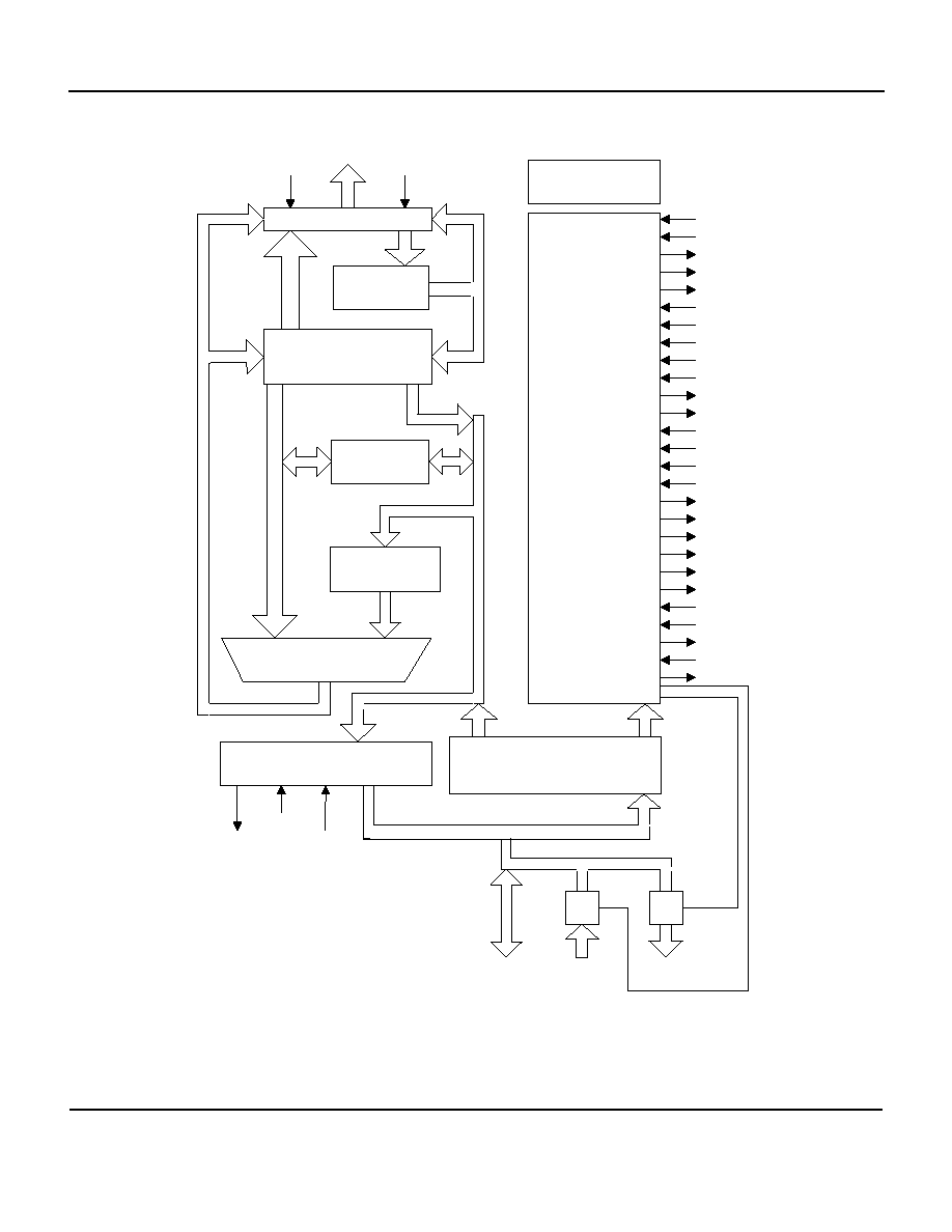
Scan control
Instruction
decoder and
logic control
Instruction pipeline
Read data register
Thumb instruction controller
Write data register
nENOUT
DBE
nENIN
B
bus
32-bit ALU
Barrel shifter
32 x 8
Multiplier
D[31:0]
AL
U
b
u
s
Register bank
(31 x 32-bit registers)
(6 status registers)
A
bus
Address
incrementer
Address register
P
C
bus
A[31:0]
ALE
ABE
I
n
c
r
em
ent
er
bus
DBGRQI
BREAKPTI
DBGACK
ECLK
nEXEC
ISYNC
BL[3:0]
APE
MCLK
nWAIT
nRW
MAS[1:0]
nIRQ
nFIQ
nRESET
ABORT
nTRANS
nMREQ
nOPC
SEQ
LOCK
nCPI
CPA
CPB
nM[4:0]
TBE
TBIT
1
En
DIN[31:0]
DOUT[31:0]
Figure 1 ARM7TDMI core diagram

ARM7TDMI
ARM DVI 0027B
Page 3
© Copyright ARM Limited 2000, 2001. All rights reserved.
Architecture
The ARM7TDMI core is based on the
von Neumann architecture with a
32-bit data bus that carries both
instructions and data. Load, store,
and swap instructions can access
data from memory. Data can be 8-bit,
16-bit, and 32-bit.
Instruction pipeline
The ARM7TDMI core uses a
three-stage pipeline to increase the
flow of instructions to the processor.
This allows multiple simultaneous
operations to take place and
continuous operation of the
processing and memory systems.
The instructions are executed in three
stages:
∑ Fetch
∑ Decode
∑ Execute.
Memory interface
The ARM7TDMI memory interface is
designed to allow optimum
performance potential and minimize
memory usage. Speed critical control
signals are pipelined to allow system
control functions to exploit the fast-
burst access modes supported by
many memory technologies.
The ARM7TDMI has four basic types
of memory cycle:
∑ internal
∑ nonsequential
∑ sequential
∑ coprocessor register transfer.
There is also the option to use either a
single bidirectional data bus or two
separate unidirectional data input and
output buses.
Memory formats
The ARM7TDMI can be configured to
treat stored words in either big-endian
or little-endian format.
Performance, code density
and operating states
The ARM7TDMI core supports two
operating states and instruction sets:
∑ ARM state for 32-bit, word-aligned
instructions
∑ Thumb state for 16-bit,
halfword-aligned instructions.
The ARM instruction set allows a
program to achieve maximum
performance with the minimum
number of instructions.
The simpler Thumb instruction set
offers much increased code density
reducing memory requirement. Code
can switch between the ARM and
Thumb instruction sets on any
procedure call.
The majority of ARM7TDMI
instructions are executed in a single
cycle. These are shown in Table 1 on
page 4.
Operating modes
The ARM7TDMI core has seven
modes of operation:
∑ User mode is the usual program
execution state
∑ Fast interrupt (FIQ) mode supports
data transfer or channel processes
to allow very fast interrupt
processing and to preserve values
across interrupt calls
∑ Interrupt (IRQ) mode is used for
general purpose interrupt handling
∑ Supervisor mode is a protected
mode for the operating system
∑ Abort mode is entered after a data
or instruction prefetch abort
∑ System mode is a privileged user
mode for the operating system
∑ Undefined mode is entered when
an undefined instruction is
executed.
Coprocessors
Up to 16 coprocessors can be
connected to an ARM7TDMI system.
Debug features
The ARM7TDMI processor core
incorporates hardware extensions for
advanced debugging features to
simplify the development of
application software, operating
systems, and hardware. The debug
extensions allow the core to be forced
into debug state.
The internal state of the ARM7TDMI
core can be examined using a JTAG
interface to allow the insertion of
instructions into the core pipeline and
avoid using the external data bus.
A typical debug system comprises:
∑ a debug host (a computer running a
toolkit from ARM or third party)
∑ a protocol converter to serve as the
communications point between the
high-level commands issued by the
debug host and the low-level
commands of the JTAG interface
∑ the target core, ARM7TDMI.
The ARM7TDMI core includes an
internal functional unit known as the
EmbeddedICE Logic. The
EmbeddedICE Logic is configured to
monitor ARM7TDMI core activity for
specific instruction fetches and data
accesses. Execution halts when the
values pre-programmed match the
current values causing a breakpoint or
watchpoint, respectively.
Configuration is done through a
dedicated scan chain via the JTAG
interface.
The ARM7TDMI can also be
connected to an Embedded Trace
Macrocell (ETM). The ETM provides
comprehensive debug and trace
facilities by allowing information on
the processor's state to be captured
before and after a specific event,
whilst the core runs at full speed. A
dedicated, configurable trace port and
FIFO allow the compressed trace data
to be read out by an external Trace
Port Analyser without affecting the
processor.

ARM7TDMI
Page 4
ARM DVI 0027B
© Copyright ARM Limited 2000, 2001. All rights reserved.
Instruction speed
summary
Due to the pipelined architecture of
the CPU, instructions overlap
considerably. In a typical cycle, one
instruction can be using the data path
while the next is being decoded and
the one after that is being fetched. For
this reason Table 1 presents the
incremental number of cycles
required by an instruction, rather than
the total number of cycles for which
the instruction uses part of the
processor. Elapsed time, in cycles, for
a routine can be calculated from the
figures listed in Table 1. These figures
assume that the instruction is actually
executed. Unexecuted instructions
take one sequential cycle.
In Table 1:
∑ n is the number of words
transferred
∑ m is 1 if bits [32:8] of the multiplier
operand are all zero or all one
∑ m is 2 if bits [32:16] of the multiplier
operand are all zero or all one
∑ m is 3 if bits [31:24] of the multiplier
operand are all zero or all one
∑ b is the number of cycles spent in
the coprocessor busy-wait loop
∑ N is a nonsequential memory cycle
∑ S is a sequential memory cycle
∑ I is an internal memory cycle
∑ C is a coprocessor register transfer
memory cycle.
Table 1 ARM instruction speed summary
Instruction
Cycle count
Additional
Data Processing
1S
+ 1I for SHIFT(Rs)
+ 1S + 1N if R15 written
MSR, MRS
1S
-
LDR
1S+1N+1I
+ 1S + 1N if R15 loaded
STR
2N
-
LDM
nS+1N+1I
+ 1S + 1N if R15 loaded
STM
(n-1)S+2N
-
SWP
1S+2N+1I
-
B,BL
2S+1N
-
SWI
2S+1N
-
MUL,MLA
1S+mI
-
MUL
1S+mI
-
MLA
1S+(m+1)I
-
MULL
1S+(m+1)I
-
MLAL
1S+(m+2)I
-
CDP
1S+bI
-
LDC,STC
(n-1)S+2N+bI
-
MCR
1N+bI+1C
-
MRC
1S+(b+1)I+1C
-

ARM7TDMI
ARM DVI 0027B
Page 5
© Copyright ARM Limited 2000, 2001. All rights reserved.
Signals
Table 2 lists and describes all of the
signals used for the ARM7TDMI.
Table 2 Signal Descriptions
Name
Type
Description
A[31:0]
Address bus
Output
This is the 32-bit
address bus. ALE, ABE and APE are used to control when the address bus is
valid.
ABE
Address bus
enable
Input
The address bus drivers are disabled when this is LOW, putting the address bus into a high
impedance state. This also controls the LOCK, MAS[1:0], nRW, nOPC, and nTRANS signals in
the same way. ABE must be tied HIGH if there is no system requirement to disable the address
drivers.
ABORT
Memory abort
Input
The memory system uses this signal to tell the processor that a requested access is not allowed.
ALE
Address latch
enable
Input
This signal is provided for backwards compatibility with older ARM processors; for new designs, if
address re-timing is required, ARM recommends the use of APE, and for ALE to be connected
HIGH.
The address bus, LOCK, MAS[1:0], nRW, nOPC, and nTRANS signals are latched when this is
held LOW. This allows these address signals to be held valid for the complete duration of a
memory access cycle. For example, when interfacing to ROM, the address must be valid until
after the data has been read.
APE
Address timing
pipeline enable
Input
Selects whether the address bus, LOCK, MAS[1:0], nRW, nTRANS, and nOPC signals operate
in pipelined (APE is HIGH) or de-pipelined mode (APE is LOW).
Pipelined mode is particularly useful for DRAM systems, where it is desirable to provide the
address to the memory as early as possible, to allow longer periods for address decoding and the
generation of DRAM control signals. In this mode, the address bus does not remain valid to the
end of the memory cycle.
De-pipelined mode can be useful for SRAM and ROM access. Here the address bus, LOCK,
MAS[1:0], nRW, nTRANS, and nOPC signals must be kept stable throughout the complete
memory cycle. However, this does not provide optimum performance.
BIGEND
Big-endian
configuration
Input
Selects how the processor treats bytes in memory: HIGH for big-endian format; LOW for
little-endian.
BL[3:0]
Byte latch control
Input
The values on the data bus is latched on the falling edge of MCLK when these signals are HIGH.
For most designs these signals should be tied HIGH.
BREAKPT
Breakpoint
Input
A conditional request for the processor to enter debug state is made by placing this signal HIGH.
If the memory access at that time is an instruction fetch, the processor enters debug state only if
the instruction reaches the execution stage of the pipeline.
If the memory access is for data, the processor enters debug state after the current instruction
completes execution. This allows extension of the internal breakpoints provided by the
EmbeddedICE logic.
BUSDIS
Bus disable
Output
When INTEST is selected on scan chain 0, 4, or 8 this is HIGH. It can be used to disable external
logic driving onto the bidirectional data bus during scan testing. This signal changes after the
falling edge of TCK.