 | –≠–ª–µ–∫—Ç—Ä–æ–Ω–Ω—ã–π –∫–æ–º–ø–æ–Ω–µ–Ω—Ç: ARM922T | –°–∫–∞—á–∞—Ç—å:  PDF PDF  ZIP ZIP |
Product Overview
Æ
ARM922TTM with AHB
System-on-Chip Platform OS Processor
ARM DVI 0025B
© Copyright ARM Limited 2001. All rights reserved
Page 1
ARM922T (Rev 1)
Applications
∑
Devices running:
- EPOC
- PalmOS
- Linux
- WindowsCE
- QNX
∑
High-performance
wireless devices
∑
Networking
applications
∑
Digital set-top boxes
∑
Imaging systems
∑
Automotive control
solutions
∑
Audio and video
encode and decode.
Benefits
∑
Designed specifically
for System-on-Chip
integration
∑
Supports the Thumb
Æ
instruction set offering
the same excellent
code density as the
ARM7TDMI cores
∑
High performance lets
system designers
integrate more
functionality into price
and power-sensitive
applications
∑
Cached processor with
an easy-to-use lower
frequency on-chip
system bus interface.
ARM922T characteristics on typical 0.18
µm process
(preliminary figures)
Die area
6.55mm
2
Power (typical)
0.8mW/MHz @ 1.8V
Clock frequency and performance
(worst-case on slow silicon, and 125∞C)
220MIPS @ 200MHz
The ARM922T (Rev 1) with AHB
The ARM922T macrocell is a high-performance 32-bit RISC integer
processor combining an ARM9TDMITM processor core with:
∑
8KB instruction cache and 8KB data cache
∑
instruction and data Memory Management Unit (MMU)
∑
write buffer with 16 data words and 4 addresses
∑
Advanced Microprocessor Bus Architecture (AMBATM) AHB interface
∑
Embedded Trace Macrocell (ETM) interface
∑
EXTEST-compatible boundary scan chain.
High performance
The ARM922T macrocell provides a high-performance processor
solution for open systems requiring full virtual memory management
and sophisticated memory protection. The ARM922T processor core
is capable of running at 200MHz on the TSMC 0.18
µm process.
Low power consumption
The ARM922T custom-designed hard macrocell has a very small die
size and very low power consumption. The integrated cache helps to
significantly reduce memory bandwidth demands, improving
performance and minimizing power consumption.
At 200MHz the ARM922T macrocell typically consumes as little as
180mW, making it ideal for many high-performance battery-powered
consumer applications. This extremely low power consumption is
essential for hand-held products supporting complex MP3, Java and
video decoding, while concurrently executing baseband protocol
software.
High levels of integration on-chip can be achieved because of the very
low power dissipation characteristics.
Page 2
© Copyright ARM Limited 2001. All rights reserved
ARM DVI 0025B
ARM922T (Rev 1)
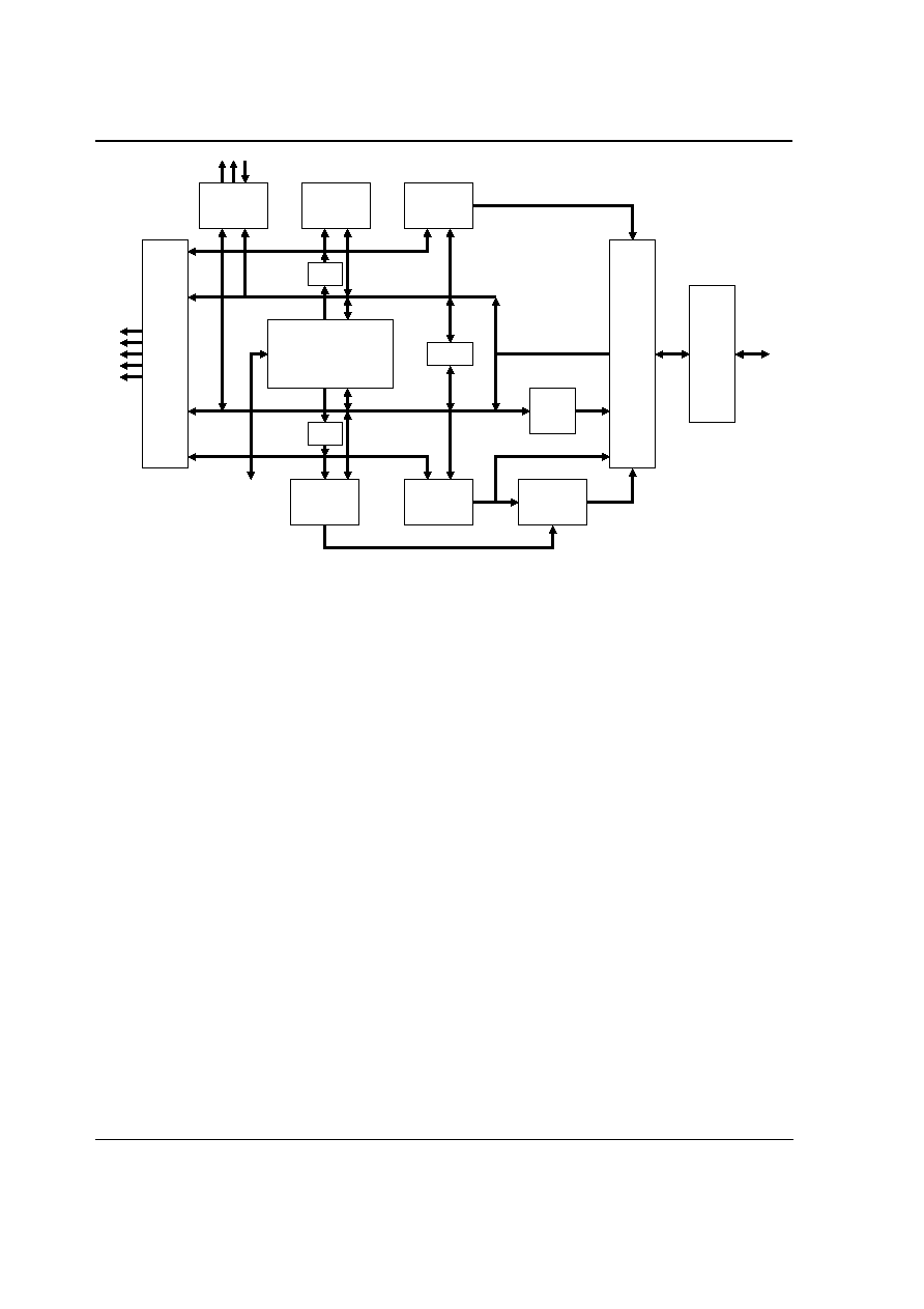
ARM922T with AHB
ARM922T macrocell
The ARM922T macrocell is
based on the ARM9TDMI
Harvard architecture processor
core, with an efficient five-stage
pipeline.
To reduce the effect of main
memory bandwidth and latency
on performance, the ARM922T
macrocell includes separate
caches and MMUs for both
instructions and data. It also has
a write buffer and physical
address TAG RAM.
Caches
Two 8KB caches are
implemented, one for
instructions, the other for data,
both with an 8-word line size.
Separate buses connect each
cache to the ARM9TDMI core
permitting a 32-bit instruction to
be fetched and fed into the
Decode stage of the pipeline at
the same time as a 32-bit data
access for the Memory stage of
the pipeline.
Cache lock-down is provided to
permit critical code sequences to
be locked into the cache to
ensure predictability for real-time
code. The cache replacement
algorithm can be selected by the
operating system as either
pseudo-random or round-robin.
Both caches are 64-way
set-associative. Lock-down
operates on a per-way basis.
Write buffer
The ARM922T macrocell also
incorporates a 16-data,
4-address write buffer to avoid
stalling the processor when
writes to external memory are
performed.
PA TAG RAM
The ARM922T macrocell
implements a Physical Address
Tag RAM (PA TAG RAM) to
perform write-backs from the
data cache.
The physical addresses of all the
lines held in the data cache are
stored by the PA TAG memory,
removing the requirement for
address translation when
evicting a line from the cache.
MMU
The ARM922T macrocell
implements an enhanced
ARMv4 MMU to provide
translation and access
permission checks for the
instruction and data address
ports of the ARM9TDMI core.
External
coprocessor
interface
ARM9TDMI
Processor core
(Integral EmbeddedICE)
Write
buffer
ID[31:0]
IMVA[31:0]
WBPA[31:0]
DPA[31:0]
IPA[31:0]
ASB
Write back
PA TAG RAM
CP15
R13
IVA[31:0]
DVA[31:0]
JTAG
DD[31:0]
Instruction
cache
Instruction
MMU
Data
MMU
Data
cache
R13
DINDEX[5:0]
Trace
interface
port
AMBA
interface
DMVA[31:0]
AHB
wrapper
AHB
Figure 1 ARM922T Functional Diagram

ARM DVI 0025B
© Copyright ARM Limited 2001. All rights reserved
Page 3
ARM922T (Rev 1)
ARM922T with AHB
The MMU features are:
∑
standard ARMv4 MMU mapping
sizes, domains, and access
protection scheme
∑
mapping sizes are 1MB
sections, 64KB large pages,
4KB small pages, and new 1KB
tiny pages
∑
access permissions for sections
∑
access permissions for large
pages and small pages can be
specified separately for each
quarter of the page (subpages)
∑
access permissions for tiny
pages
∑
16 domains implemented in
hardware
∑
64-entry instruction Translation
Lookaside Buffer (TLB) and
64-entry data TLB
∑
hardware page table walks
∑
round-robin replacement
algorithm (also called cyclic).
Control coprocessor
(CP15)
The control coprocessor is
provided for configuration of the
caches, the write buffer, and
other ARM922T options.
Eleven registers are available for
program control:
∑
Register 1 controls system
operation parameters including
endianness, cache, and MMU
enable
∑
Registers 2 and 3 configure and
control MMU functions
∑
Registers 5 and 6 provide MMU
status information
∑
Registers 7 and 9 are used for
cache maintenance operations
∑
Registers 8 and 10 are used for
MMU maintenance operations
∑
Register 13 is used for fast
context switching
∑
Register 15 is used for test.
ARM9TDMI Embedded
Trace Macrocell (ETM9)
interface
The ETM interface permits the
connection of an ETM9 to
provide the capacity to trace
instructions and data accesses
in real time.
Real-time trace is made up of
three elements:
∑
an Embedded Trace Macrocell
(ETM)
∑
a Trace Port Analyzer (TPA)
∑
the Trace Debug Tools (TDT)
extensions to the ARM
Developer Suite.
Debug features
The ARM9TDMI processor core
incorporates an EmbeddedICE
unit and EmbeddedICE-RT logic
permitting both software tasks
and external debug hardware to:
∑
set hardware and software
breakpoints
∑
perform single-stepping
∑
enable access to registers and
memory.
This functionality is implemented
as a coprocessor and is
accessible from hardware
through the JTAG port.
Full-speed, real-time execution
of the processor is maintained
until a breakpoint is hit.
At this point control is passed
either to a software handler or to
JTAG control.
Coprocessors
The ARM9TDMI coprocessor
interface permits full
independent processing of the
ARM execution pipeline and
supports up to 16 independent
coprocessors. Four of these
coprocessors are available for
designer-specified purposes,
such as for floating-point math
operations, and signal
processing.
32-bit data buses
The ARM9TDMI core provides
32-bit data buses:
∑
between the processor core and
the instruction cache
∑
between the processor core and
the data cache
∑
between coprocessors and the
processor core.
This enables the ARM9TDMI
core to achieve very high
performance on many code
sequences, especially those that
require data movement in
parallel with data processing.

The ARMv4T Architecture
Page 4
© Copyright ARM Limited 2001. All rights reserved
ARM DVI 0025B
ARM922T (Rev 1)
The ARM9TDMI core
The ARM9TDMI processor core
implements the ARMv4T
Instruction Set Architecture
(ISA). The ARMv4T ISA is a
superset of the ARMv4 ISA
(implemented by the
StrongARMÆ processor) with
additional support for the Thumb
16-bit compressed instruction
set. The ARMv4T ISA is
implemented by the ARM7TM
Thumb family. This gives full
upward compatibility to the
ARM9TM Thumb family.
Performance and code
density
The ARM9TDMI core executes
two instruction sets:
∑
32-bit ARM instruction set
∑
16-bit Thumb instruction set.
The ARM instruction set is
designed so that a program can
achieve maximum performance
with the minimum number of
instructions. Most ARM9TDMI
instructions are executed in a
single cycle.
The simpler Thumb instruction
set offers much increased code
density reducing code size and
memory requirement.
Code can switch between the
ARM and Thumb instruction sets
on any procedure call.
ARM9TDMI integer
pipeline stages
The integer pipeline consists of
five stages to maximize
instruction throughput in the
ARM9TDMI core:
1.
Fetch
2.
Decode and register read
3.
Execute shift and ALU
operation, or address
calculate, or multiply
4.
Memory access and multiply
5.
Write register.
By using a five-stage pipeline,
the ARM922T delivers a
throughput approaching one
instruction per cycle.
Registers
The ARM9TDMI processor core
consists of a 32-bit datapath and
associated control logic. This
datapath contains 31 general-
purpose registers, coupled to a
full shifter, Arithmetic Logic Unit,
and a multiplier. At any one time
16 registers are visible to the
user. The remainder are mode-
specific replacement registers
(banked registers) used to speed
up exception processing, and to
make nested exceptions
possible.
Register 15 is the Program
Counter (PC) that can be used in
all instructions to reference data
relative to the current instruction.
R14 holds the return address
after a subroutine call. R13 is
used (by software convention) as
a stack pointer.
Exception types/Modes
The ARM9TDMI core supports
five types of exception, and a
privileged processing mode for
each type. The types of
exceptions are:
∑
fast interrupt (FIQ)
∑
normal interrupt (IRQ)
∑
memory aborts (used to
implement memory protection or
virtual memory)
∑
attempted execution of an
undefined instruction
∑
software interrupts (SWIs).
All exceptions have banked
registers for R14 and R13. After
an exception, R14 holds the
return address for exception
processing. This address is used
both to return after the exception
is processed and to address the
instruction that caused the
exception.
R13 is banked across exception
modes to provide each exception
handler with a private stack
pointer. The fast interrupt mode
also banks registers 8 to 12 so
that interrupt processing can
begin without the need to save or
restore these registers.
A seventh processing mode,
System mode, uses the User
mode registers. System mode
runs tasks that require a
privileged processor mode and
enables them to invoke all
classes of exceptions.
Status registers
All other processor states are
held in status registers. The
current operating processor
status is in the Current Program
Status Register (CPSR). The
CPSR holds:
∑
four ALU flags (Negative, Zero,
Carry, and Overflow)
∑
an interrupt disable bit for each
of the IRQ and FIQ interrupts
∑
a bit to indicate ARM or Thumb
execution state
∑
five bits to encode the current
processor mode.
All five exception modes also
have a Saved Program Status
Register (SPSR) that holds the
CPSR of the task immediately
before the exception occurred.

The ARMv4T Architecture
ARM DVI 0025B
© Copyright ARM Limited 2001. All rights reserved
Page 5
ARM922T (Rev 1)
Conditional execution
All ARM instructions can be
executed conditionally and can
optionally update the four
condition code flags (Negative,
Zero, Carry, and Overflow)
according to their result. Fifteen
conditions are implemented.
Classes of instruction
The ARM and Thumb instruction
sets can be divided into four
broad classes of instruction:
∑
data processing instructions
∑
load and store instructions
∑
branch instructions
∑
coprocessor instructions.
Data processing
instructions
The data processing instructions
operate on data held in
general-purpose registers. Of
the two source operands, one is
always a register. The other has
two basic forms:
∑
an immediate value
∑
a register value optionally
shifted.
If the operand is a shifted
register, the shift can be an
immediate value or the value of
another register. Four types of
shift can be specified. Most data
processing instructions can
perform a shift followed by a
logical or arithmetic operation.
There are two classes of multiply
instructions:
∑
normal, 32-bit result
∑
long, 64-bit result variants.
Both types of multiply instruction
can optionally perform an
accumulate operation.
Load and store
instructions
There are two main types of load
and store instructions:
∑
load or store the value of a
single register
∑
load or store multiple register
values.
Load and store single register
instructions can transfer a 32-bit
word, a 16-bit halfword, or an
8-bit byte between memory and
a register. Byte and halfword
loads can be automatically zero
extended or sign extended as
they are loaded. These
instructions have three primary
addressing modes:
∑
offset
∑
pre-indexed
∑
post-indexed.
The address is formed by adding
an immediate, or register- based,
positive, or negative offset to a
base register. Register-based
offsets can also be scaled with
shift operations. Pre-indexed
and post-indexed addressing
modes update the base register
with the base plus offset
calculation.
As the PC is a general-purpose
register, a 32-bit value can be
loaded directly into the PC to
perform a jump to any address in
the 4GB memory space.
Load and store multiple
instructions perform a block
transfer of any number of the
general purpose registers to, or
from, memory. Four addressing
modes are provided:
∑
pre-increment addressing
∑
post-increment addressing
∑
pre-decrement addressing
∑
post-decrement addressing.
The base address is specified by
a register value (that can be
optionally updated after the
transfer). As the subroutine
return address and the PC
values are in general-purpose
registers, very efficient
subroutine calls can be
constructed.
Branch instructions
As well as letting data
processing or load instructions
change control flow (by writing
the PC) a standard branch
instruction is provided with 24-bit
signed offset, providing for
forward and backward branches
of up to 32MB.
A branch with link (BL)
instruction enables efficient
subroutine calls. BL preserves
the address of the instruction
after the branch in R14 (the Link
Register or LR). This lets a move
instruction put the LR in to the
PC and return to the instruction
after the branch.
The branch and exchange (BX)
instruction switches between
ARM and Thumb instruction sets
with the return address optionally
preserving the operating mode of
the calling routine.
Coprocessor
instructions
There are three types of
coprocessor instructions:
∑
coprocessor data processing
instructions
∑
coprocessor register transfer
instructions
∑
coprocessor data transfer
instructions.