
DC-DC CONVERTERS POLA Non-isolated
1
NEW Product
File Name: pth12010.pdf Rev (07): 19 Dec 2005
2 YEAR WARRANTY
All specifications are typical at nominal input, full load at 25 ∞C unless otherwise stated
C
in
= 560 µF, C
out
= 0 µF
SPECIFICATIONS
*Auto-trackTM is a trade mark of
Texas Instruments
The PTH12010 is a next generation series of non-isolated dc-dc converters offering some
of the most advanced POL features available in the industry. The primary new feature
provides for sequencing between multiple modules, a function, which is becoming a
necessity for powering advanced silicon including DSP's, FPGA's and ASIC's requiring
controlled power-up and power-down. Other industry leading features include margin
up/down controls and efficiencies up to 94%. The PTH12010 has an input voltage of
10.8 Vdc to 13.2 Vdc
and offers a wide 1.2 Vdc to 5.5 Vdc output voltage range with up to
12 A output current, which allows for maximum design flexibility and a pathway for future
upgrades.
∑
12 A output current
∑
12 V input voltage
∑
Wide-output voltage adjust
∑
1.2 Vdc to 5.5 Vdc for suffix `W' and
0.8 Vdc to 1.8 Vdc for suffix `L'
∑
Auto-trackTM sequencing*
∑
Margin up/down controls
∑
Efficiencies up to 94%
∑
Output ON/OFF inhibit
∑
Output voltage sense
∑
Point-of-Load-Alliance (POLA) compatible
∑
Available RoHS compliant
PTH12010
1 2 V i n s i n g l e o u t p u t
International Safety Standard Approvals
UL/cUL CAN/CSA-C22.2 No. 60950-1-03/UL 60950-1,
File No. E174104
TÐV Product Service (EN60950) Certificate No. B 04 06 38572 044
CB Report and Certificate to IEC60950, Certificate No.
US/8292/UL
OUTPUT SPECIFICATIONS
Voltage adjustability
Suffix `-W'
1.2-5.5 Vdc
(See Note 4)
Suffix `-L'
0.8-1.8 Vdc
Setpoint accuracy
±2.0% Vo
Line regulation
±10 mV typ.
Load regulation
±12 mV typ.
Total regulation
±3.0% Vo
Minimum load
0 A
Ripple and noise
Suffix `-W'
25 mV pk-pk
20 MHz bandwidth
Suffix `-L'
25 mV pk-pk
Temperature co-efficient
-40 ∫C to +85 ∫C
±0.5% Vo
Transient response
70 µs recovery time
(See Note 5)
Overshoot/undershoot 100 mV
Margin adjustment
±5.0% Vo
INPUT SPECIFICATIONS
Input voltage range
(See Note 3)
10.8-13.2 Vdc
Input current
No load
10 mA typ.
Remote ON/OFF
(See Note 1)
Positive logic
Start-up time
1 V/ms
Undervoltage lockout
9.0-9.5 V typ.
Track input voltage
Pin 8 (See Note 6)
±0.3 Vin
EMC CHARACTERISTICS
Electrostatic discharge
EN61000-4-2, IEC801-2
Conducted immunity
EN61000-4-6
Radiated immunity
EN61000-4-3
GENERAL SPECIFICATIONS
Efficiency
See Tables on page 2
Insulation voltage
Non-isolated
Switching frequency
Suffix `-W'
300 kHz to 400 kHz
Suffix `-L'
200 kHz to 300 kHz
Approvals and
EN60950
standards
UL/cUL60950
Material flammability
UL94V-0
Dimensions
(L x W x H)
34.80 x 15.75 x 9.00 mm
1.370 x 0.620 x 0.354 in
Weight
5 g (0.18 oz)
MTBF
Telcordia SR-332
7,092,000 hours
ENVIRONMENTAL SPECIFICATIONS
Thermal performance
Operating ambient,
-40 ∫C to +85 ∫C
(See Note 2)
temperature
Non-operating
-40 ∫C to +125 ∫C
MSL (`Z' suffix only)
JEDEC J-STD-020C
Level 3
PROTECTION
Short-circuit
Auto reset
20 A typ.

File Name: pth12010.pdf Rev (07): 19 Dec 2005
For the most current data and application support visit www.artesyn.com/powergroup/products.htm
DC-DC CONVERTERS POLA Non-isolated
2
NEW Product
N
No
otte
es
s
1
Remote ON/OFF. Positive Logic
ON:
Pin 3 open; or V > Vin - 0.5 V
OFF:
Pin 3 GND; or V < 0.8 V (min - 0.2 V).
2
See Figures 1, 2 and 3 for safe operating curves for the PTH12010W and
Figures 6 and 7 for PTH12010L.
3
A 560 µF electrolytic input capacitor is required for proper operation. The
capacitor must be rated for a minimum of 800 mA rms of ripple current.
4
An external output capacitor is not required for basic operation. Adding
330 µF of distributed capacitance at the load will improve the transient
response.
5
1 A/µs load step, 50 to 100% I
omax
, C
out
= 330 µF.
6
If utilized Vout will track applied voltage by ±0.3 V (up to Vo set point).
7
Tape and reel packaging only available on the surface-mount versions.
8
To order Pb-free (RoHS compatible) surface-mount parts replace the
mounting option `S' with `Z', e.g. PTH12010WAZ. To order Pb-free
(RoHS compatible) through-hole parts replace the mounting option `H'
with `D', e.g. PTH12010WAD.
9
NOTICE: Some models do not support all options. Please contact your
local Artesyn representative or use the on-line model number search tool at
http://www.artesyn.com/powergroup/products.htm to find a suitable
alternative.
P T H 1 2 0 1 0 W A S T
Part Number System with Options
Product Family
Point of Load Alliance
Compatible
The ultra-wide output voltage trim range offers major advantages to users who
select the PTH12010. It is no longer necessary to purchase a variety of
modules in order to cover different output voltages. The output voltage can be
trimmed in a range of 1.2 V to 5.5 V for suffix `W' and 0.8 Vdc to 1.8 Vdc for
suffix `L'. When the PTH12010 converter leaves the factory the output has
been adjusted to the default voltage of 1.2 V for the PTH12010W and 0.8 V for
PTH12010L.
O
Ou
uttp
pu
utt V
Vo
olltta
ag
ge
e A
Ad
djju
us
sttm
me
en
ntt o
off tth
he
e P
PT
TH
H1
12
20
01
10
0 S
Se
erriie
es
s
Output Current
01 = 12 A
Packaging Options
No Suffix = Trays
T = Tape and Reel
(7)
Input Voltage
12 = 12 V
Mechanical Package
Always 0
Output Voltage Code
W = Wide, L = Low Voltage
Pin Option
A = Through-Hole Std. Pin Length (0.140")
A = Surface-Mount Tin/Lead Solder Ball
PTH12010
1 2 V i n s i n g l e o u t p u t
Mounting Optionl
(8)
D = Horizontal Through-Hole (Matte Sn)
H = Horizontal Through-Hole (Sn/Pb)
S = Surface-Mount (63/37 Sn/Pb
pin solder material)
Z = Surface-Mount (96.5/3.0/0.5 Sn/Ag/Cu
pin solder material)
EFFICIENCY TABLE - PTH12010L (I
O
= 8 A)
OUTPUT VOLTAGE
EFFICIENCY
Vo = 1.8 V
89%
Vo = 1.5 V
88%
Vo = 1.2 V
86%
Vo = 1.0 V
84%
Vo = 0.8 V
82%
EFFICIENCY TABLE - PTH12010W
(I
O
= 8 A)
OUTPUT VOLTAGE
EFFICIENCY
Vo = 5.0 V
94%
Vo = 3.3 V
93%
Vo = 2.5 V
91%
Vo = 2.0 V
90%
Vo = 1.8 V
89%
Vo = 1.5 V
88%
Vo = 1.2 V
86%
OUTPUT
INPUT
OUTPUT
OUTPUT
OUTPUT
EFFICIENCY
REGULATION
MODEL
POWER
VOLTAGE
VOLTAGE
CURRENT
CURRENT
(MAX.)
LINE
LOAD
NUMBER
(8,9)
(MAX.)
(MIN.)
(MAX.)
66 W
10.8-13.2 Vdc
0.8-1.8 Vdc
0 A
12 A
89%
±10 mV
±12 mV
PTH12010L
66 W
10.8-13.2 Vdc
1.2-5.5 Vdc
0 A
12 A
94%
±10 mV
±12 mV
PTH12010W
File Name: pth12010.pdf Rev (07): 19 Dec 2005
For the most current data and application support visit www.artesyn.com/powergroup/products.htm
DC-DC CONVERTERS POLA Non-isolated
3
NEW Product
TEMPERA
TURE (∫C)
Nat conv
100 LFM
200 LFM
400 LFM
OUTPUT CURRENT (A)
20
30
40
50
60
70
80
90
0
2
4
6
8
10
12
TEMPERA
TURE (∫C)
Nat conv
100 LFM
200 LFM
400 LFM
OUTPUT CURRENT (A)
20
30
40
50
60
70
80
90
0
2
4
6
8
10
12
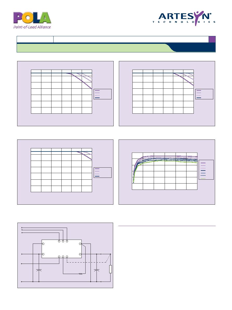
Figure 2 - Safe Operating Area
Vin = 12 V, Output Voltage = 3.3 V (See Note A)
Figure 1 - Safe Operating Area
Vin = 12 V, Output Voltage = 5 V (See Note A)
EFFICIENCY (%)
OUTPUT CURRENT (A)
5.0V
3.3V
2.5V
2.0V
1.8V
1.5V
40
50
60
70
80
90
100
0
2
4
6
8
10
12
1.2V
Vout
Figure 4 - Efficiency vs Load Current
Vin = 12 V (See Note B)
TEMPERA
TURE (∫C)
Nat conv
100 LFM
200 LFM
400 LFM
OUTPUT CURRENT (A)
20
30
40
50
60
70
80
90
0
2
4
6
8
10
12
Figure 3 - Safe Operating Area
Vin = 12 V, Output Voltage 1.8 V (See Note A)
PTH12010
1 2 V i n s i n g l e o u t p u t
N
No
otte
es
s
A
SOA curves represent the conditions at which internal components are
within the Artesyn derating guidelines.
B
Characteristic data has been developed from actual products tested at
25 ∞C. This data is considered typical data for the converter.
PTH12010W Characteristic Data
Track
8
9
10
PTH12010
(Top View)
Margin Up
Margin Down
5
4
3
6
7
2
1
GND
GND
L
O
A
D
C
in
560
µF
(Required)
+
V
in
Inhibit
C
out
330
µF
(Optional)
+
R
SET
1%, 0.1W
(Required)
V
out
V
o
Sense
Figure 5 - Standard Application
For the most current data and application support visit www.artesyn.com/powergroup/products.htm
DC-DC CONVERTERS POLA Non-isolated
4
NEW Product
File Name: pth12010wl.pdf Rev (06): 07 Feb 2005
PTH12010
1 2 V i n s i n g l e o u t p u t
TEMPERA
TURE (∫C)
OUTPUT CURRENT (A)
20
30
40
50
60
70
80
90
0
2
4
6
8
10
Nat conv
100 LFM
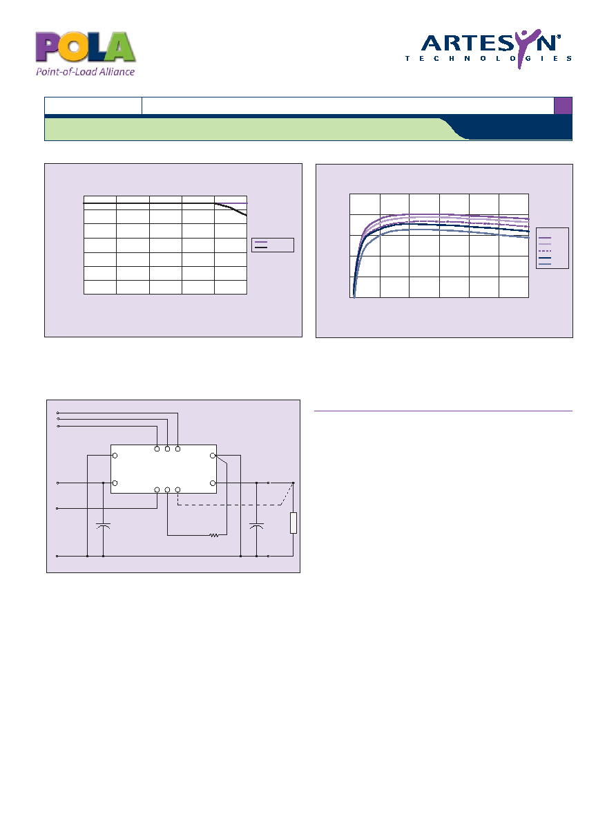
Figure 6 - Safe Operating Area
Vin = 12 V, Output Voltage 1.8 V (See Note A)
N
No
otte
es
s
A
SOA curves represent the conditions at which internal components are
within the Artesyn derating guidelines.
B
Characteristic data has been developed from actual products tested at
25 ∞C. This data is considered typical data for the converter.
EFFICIENCY (%)
OUTPUT CURRENT (A)
1.8V
1.5V
1.2V
1.0V
0.8V
50
60
70
80
90
100
0
2
4
6
8
10
Vout
12
Figure 7 - Efficiency vs Load Current
Vin = 12 V (See Note B)
PTH12010L Characteristic Data
Track
8
9
10
PTH12010
(Top View)
Margin Up
Margin Down
5
4
3
6
7
2
1
GND
GND
L
O
A
D
C
in
560
µF
(Required)
+
V
in
Inhibit
C
out
330
µF
(Optional)
+
R
SET
1%, 0.1W
(Required)
V
out
V
o
Sense
Figure 8 - Standard Application
File Name: pth12010.pdf Rev (07): 19 Dec 2005
Please consult our website for the following items:
Application Note
www.artesyn.com
Datasheet © Artesyn TechnologiesÆ 2005
The information and specifications contained in this datasheet are believed to be correct at time of publication. However, Artesyn Technologies accepts no responsibility for consequences arising
from printing errors or inaccuracies. The information and specifications contained or described herein are subject to change in any manner at any time without notice. No rights under any patent
accompany the sale of any such product(s) or information contained herein.
For the most current data and application support visit www.artesyn.com/powergroup/products.htm
DC-DC CONVERTERS POLA Non-isolated
5
NEW Product
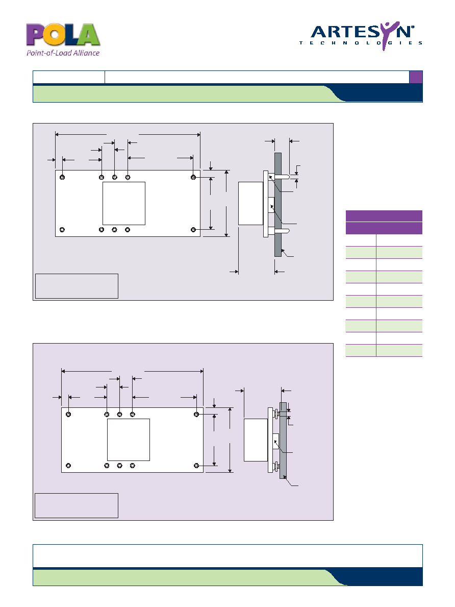
0.070 (1.78)
(Standoff Shoulder)
Lowest Component
0.010 min. (0.25)
Bottom side Clearance
TOP VIEW
SIDE VIEW
1.370 (34.80)
0.620
6
7
3
5
4
10
9
8
1
2
MAX.
0.354 (9.00)
Host Board
(15.75)
¯0.040 (1.02)
5 Places
0.375
(9.52)
0.125 (3.18)
0.625 (15.88)
0.125 (3.18)
(1.52)
0.060
(12.70)
0.500
(1.52)
0.060
(3.55)
0.140
Dimensions in Inches (mm)
Tolerances (unless otherwise specified)
2 Places
±0.030 (±0.76)
3 Places
±0.010 (±0.25)
TOP VIEW
1.370 (34.80)
0.620
6
7
3
5
4
10
9
8
1
2
(15.75)
0.375
(9.52)
0.125 (3.18)
0.625 (15.88)
0.125 (3.18)
(1.52)
0.060
(12.70)
0.500
(1.52)
0.060
Dimensions in Inches (mm)
Tolerances (unless otherwise specified)
2 Places
±0.030 (±0.76)
3 Places
±0.010 (±0.25)
Host Board
Lowest Component
0.010 min. (0.25)
Bottom side Clearance
SIDE VIEW
Solder Ball
¯0.040 (1.02)
10 Places
*After solder reflow
on customer board
0.354 (9.00)
max.*
Figure 9 - Plated Through-Hole Mechanical Drawing
Figure 10 - Surface-Mount Mechanical Drawing
*Denotes negative logic:
Open = Normal operation
Ground = Function active
PIN CONNECTIONS
PIN NO.
FUNCTION
1
Ground
2
Vin
3
Inhibit*
4
Vo adjust
5
Vo sense
6
Vout
7
Ground
8
Track
9
Margin down*
10
Margin up*
PTH12010
1 2 V i n s i n g l e o u t p u t