 | –≠–ª–µ–∫—Ç—Ä–æ–Ω–Ω—ã–π –∫–æ–º–ø–æ–Ω–µ–Ω—Ç: SIL25C | –°–∫–∞—á–∞—Ç—å:  PDF PDF  ZIP ZIP |
Document Outline
- Absolute Maximum Ratings
- Input Characteristics
- Turn On/Off
- Signal Electrical Interface
- Reliability and Service Life
- Other Specifications
- Safety Agency Approvals
- Material Ratings
- Model Numbers
- RoHS Compliance Ordering Information
- SIL25C-12SNEG-VJ
- Input Characteristics
- Electrical Characteristics - O/P
- Electrical Characteristics - O/P
- Protection and Control Features
- Efficiency
- Illustrations
- SIL25C-12SNEG-VJ
- Figure 1: Thermal De-rating Curve
- Figure 2: Efficiency vs Load and Line
- Figure 3: Short Circuit Characteristic
- Figure 4: Transient Response 50-75% - 50%, 1A/µS
- Figure 6: Typical Power Up
- Figure 7: Control On/Off
- Figure 8: Typical Ripple and Noise
- Figure 9: Mechanical Drawing
- Pinout Table
- Notes
Trim range (-4.5 Vdc to -5.5 Vdc)
High power density design means reduced board space requirement
Remote sense
Power good output signal (open collector)
Operating ambient temperature to 80 ∫C with
suitable derating and forced air cooling
Remote ON/OFF (active high)
Overtemperature protection
0 A minimum load
Input undervoltage lockout
Overcurrent and short-circuit protection
Available RoHS compliant
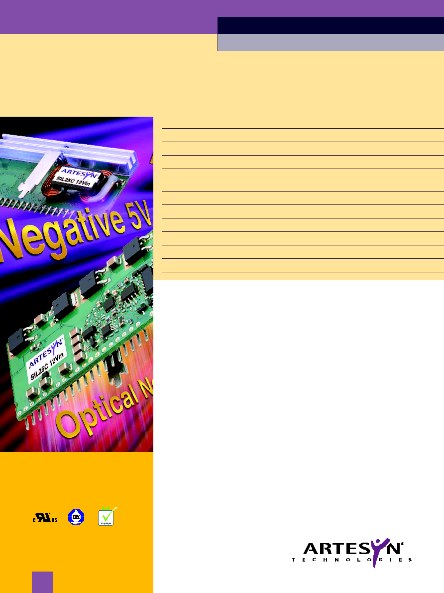
SIL25C SERIES
Single negative output
SIL25C Series | 25 A DC-DC Converter
C Class Non-Isolated
1
[ 2 YEAR WARRANTY ]
The SIL25C is a new high density non-
isolated dc-dc converter. The converter
has a wide input range (10.2 Vdc to
13.8 Vdc) and offers a -4.5 Vdc to -5.5 Vdc
output voltage range with a 25 A load. The
series offers remote ON/OFF, over-
temperature protection and over-current
protection as standard.
The remote sense feature enables the
SIL25C compensate for voltage drops
between the converters output and the load.
With full international safety approvals
including EN60950 and UL/cUL60950 the
SIL25C reduces compliance costs and time
to market.
File Name: lf_sil25c_12_neg.pdf Rev (02): 22 Dec 2005

SIL25C Series | 25 A DC-DC Converter
C Class Non-Isolated
2
Characteristic
Symbol
Min
Typ
Max
Units
Notes and Conditions
Input voltage - turn on
Vin (on)
8.5
10.0
10.2
V DC
Input voltage - turn off
Vin (off)
8.5
9.5
10.0
V DC
Turn on delay - enabled,
Tdelay
30
msec
With the Remote ON/OFF signal
then power applied
(power)
asserted, this is the time from
when the input voltage reaches
the minimum specified operating
voltage until the POWER GOOD
is asserted high
Turn on delay - power
Tdelay
20
msec
Vin = Vin (nom), then Remote
applied, then Remote ON/OFF
(Remote ON/OFF)
ON/OFF asserted. This is the
asserted
time taken until the POWER
GOOD is asserted high
Output to Power Good
Tdelay
20
msec
Output voltage in full regulation
delay
to POWER GOOD asserted high
Rise time
Trise
8
msec
From 10% to 90%; full resistive
load, 2 x 680µF external
capacitance
All specifications are typical at nominal input Vin = 12V, full load under any resistive load combination at 25∞C unless otherwise stated.
Characteristic
Symbol
Min
Typ
Max
Units
Notes and Conditions
Input voltage - operating
Vin (oper)
10.2
12.0
13.8
V DC
Input current - no load
lin
280
400
mADC
Vin (min) - Vin (max), enabled
Input current - Quiescent
lin (off)
30
40
mADC
Converter disabled
Input voltage variation
dv/dt
1.0
V/ms
Input Characteristics
Turn On/Off
Absolute Maximum Ratings
File Name: lf_sil25c_12_neg.pdf Rev (02): 22 Dec 2005
Characteristic
Symbol
Min
Typ
Max
Units
Notes and Conditions
Input voltage - continuous
Vin (cont)
-0.3
13.8
V DC
Vin(+) - Vin(-)
Operating temperature
Top
-40
80
∫C
Measured at thermal reference
points, see Note 1. Higher
ambient operation possible with
forced air cooling. See de-rating
curves
Power Good pull-up voltage
15
V
Storage temperature
Tstorage
-40
125
∫C
Output current
Iout
0
25
A

SIL25C Series | 25 A DC-DC Converter
C Class Non-Isolated
3
www.artesyn.com
Characteristic - Signal Name Symbol
Min
Typ
Max
Units
Notes and Conditions
At remote/control ON/OFF pin
See Notes 2 and 3
Open collector or equivalent
See Application Note 1
48 for
compatible
Remote ON/OFF details
Control pin open circuit voltage
Vih
2.6
4
V
Iih = 0 µA; open circuit voltage
High level input current
Iih
1
µA
Current flowing into control pin
when pin is pulled high
(max. at Vih = 13.8V)
High level input voltage
Vih
2.50
Vin
Converter guaranteed on when
control pin is greater than Vih
(max)
Low level input voltage
ViI
1.20
V
Converter guaranteed off
when control pin is
less than Vil (max)
Low level input current
Iil (max)
1.3
mA
ViI = 0.0 V;
Characteristic
Symbol
Min
Typ
Max
Units
Notes and Conditions
Mean time between failure
MTBF
282,000
Hours
MIL-HDBK-217F,
Vin = Vin (nom); Iout = Iout
(max); ambient 25∫C;
ground benign environment
Mean time between failure
MTBF
3,000,000
Hours
Telcordia SR-332
Issue 3, ground benign,
temp. = 40∫C, Vin = Vin (nom),
Iout = Iout (max)
Signal Electrical Interface
Reliability and Service Life
File Name: lf_sil25c_12_neg.pdf Rev (02): 22 Dec 2005

SIL25C Series | 25 A DC-DC Converter
C Class Non-Isolated
4
Other Specifications
Material Ratings
Characteristic - Signal Name Notes and Conditions
Flammability rating
UL94V-0
Material type
FR4 PCB
Characteristic
Symbol
Min
Typ
Max
Units
Notes and Conditions
Switching frequency
Fsw
250
kHz
Per phase, (2 phase)
Weight
28.3
g
Safety Agency Approvals
Characteristic
UL/cUL 60950 File No.
TBD
TÐV Product Service IEC 60950 Certificate No. TBD
Model Numbers
File Name: lf_sil25c_12_neg.pdf Rev (02): 22 Dec 2005
Model
Input
Output
Output Current
Typical
Max. Load
Number
Voltage
Voltage
(Max.)
Efficiency
Regulation
SIL25C-12SNEG-VJ
12VDC
-4.5V to -5.5V
25A
90%
±1.0%
RoHS Compliance Ordering Information
The `J' at the end of the
part number
indicates that the
part is Pb-free
(RoHS 6/6 compliant). TSE RoHS 5/6
(non Pb-free) compliant versions may
be available on special request, please
contact your local sales representative
for details.

SIL25C Series | 25 A DC-DC Converter
5
www.artesyn.com
C Class Non-Isolated
File Name: lf_sil25c_12_neg.pdf Rev (02): 22 Dec 2005
Input Characteristics
SIL25C-12SNEG-VJ
Electrical Characteristics - O/P
SIL25C-12SNEG-VJ
Characteristic
Symbol
Min
Typ
Max
Units
Notes and Conditions
Nominal set-point voltage
Vo (nom)
-4.85
-5.05
-5.25
V DC
Vin = Vin (nom); Iout = Iout (NL)
Worst case condition over line,
load, temperature and life
Line regulation
±1.0
%
Iout = Vin (min) to Vin (max)
Load regulation
±1.0
%
Vin = Vin (nom); Iout (min) to
Iout (max)
Output current continuous
Iout
0
25
A DC
Output current - short circuit
Isc
23.9
A rms
Continuous, unit auto recovers
from short
Output voltage - noise
Vp-p
100
mV pk-pk Measurement bandwidth 20 MHz
Vrms
50
mV rms
See Application Note 1
48 for
measurement set-up details
Characteristic
Symbol
Min
Typ
Max
Units
Notes and Conditions
Input current - operating
Iin
11.6
A DC
Vin = Vin (nom); Iout = Iout
(max.)
Reflected ripple current
Iin (ripple)
60
mA RMS
Iout = Iout (max.), measured
300
mA pk-pk with external filter. See
Application Note 1
48 for details
Input capacitance - internal
Cinput
18.8
µF
filter
Input capacitance - external
Cbypass
800
µF
Recommended customer
input
added capacitance

SIL25C Series | 25 A DC-DC Converter
C Class Non-Isolated
6
SIL25C-12SNEG-VJ
Efficiency
SIL25C-12SNEG-VJ
Characteristic
Symbol
Min
Typ
Max
Units
Notes and Conditions
Efficiency
89.0
90.4
%
Iout = 100% Iout (max),
Vin = Vin (nom)
Efficiency
90.7
92.7
%
Iout = 50% Iout (max),
Vin = Vin (nom)
SIL25C-12SNEG-VJ
Protection and Control Features
Characteristic
Symbol
Min
Typ
Max
Units
Notes and Conditions
Overcurrent limit inception
Ioc
35
A DC
Vo = 90% of Vo (nom)
Open sense voltage
-5.05
V DC
Sense pins not connected
Electrical Characteristics - O/P
Characteristic
Symbol
Min
Typ
Max
Units
Notes and Conditions
Load transient response -
Vdynamic
75
mV
Peak deviation for 50% to 75%
peak deviation
step load, di/dt = 1A/µs
Load transient response -
Trecovery
150
µsec
Settling time to within 1% of
recovery
output set point voltage for 50%
to 75% step load
External load capacitance
Cext
1360
µF
Maximum capacitor value may
vary with load conditions
File Name: lf_sil25c_12_neg.pdf Rev (02): 22 Dec 2005

SIL25C Series | 25 A DC-DC Converter
C Class Non-Isolated
7
www.artesyn.com
File Name: lf_sil25c_12_neg.pdf Rev (02): 22 Dec 2005
SIL25C-12SNEG-VJ
O
U
T
P
U
T
C
U
R
R
E
N
T
(
A
)
AMBIENT TEMPERATURE (∫C)
5
10
15
20
25
30
0
20
40
60
80
1.0m/s
1.5m/s
2.0m/s
3.0m/s
E
F
F
I
C
I
E
N
C
Y
(
%
)
OUTPUT CURRENT (A)
Low Line
Nom Line
High Line
80
82
84
86
88
90
92
94
0
5
10
15
20
25
Figure 1: Thermal De-rating Curve
Airflow Direction from Pin 24 to Pin 1
Figure 2: Efficiency vs Load and Line
Figure 3: Short Circuit Characteristic
(Channel 4: Output Current at 10A/div,
Channel 2: Output Voltage)
Figure 4: Transient Response 50-75% - 50%, 1A/µS
(Channel 2: Current load step at 5A/div,
Channel 3: Output Voltage deviation)
Figure 6: Typical Power Up
(Channel 2: DC Input, Channel 3: Output Voltage)
File Name: lf_sil25c_12_neg.pdf Rev (02): 22 Dec 2005
Figure 7: Control On/Off
(Channel 2: Remote ON/OFF, Channel 3: Output Voltage
Channel 4: Power Good)

SIL25C Series | 25 A DC-DC Converter
C Class Non-Isolated
8
SIL25C-12SNEG-VJ
Figure 8: Typical Ripple and Noise
File Name: lf_sil25c_12_neg.pdf Rev (02): 22 Dec 2005
SIL25C Series | 25 A DC-DC Converter
C Class Non-Isolated
9
www.artesyn.com
File Name: lf_sil25c_12_neg.pdf Rev (02): 22 Dec 2005
PIN 1
ID LABEL LOCATION
1
.
2
5
0
TYP.
0.100 [2.54]
0
.
1
4
0
[
3
.
5
6
]
2.400 [60.96]
0.470 [11.94]
0.158 [4.02]
0.520 [13.21]
0.260
±0.030
[6.60
±0.760]
0
.
1
4
0
[
3
.
5
6
]
[
3
1
.
7
5
]
3 Places 0.010 (0.250)
Tolerances (unless otherwise specified)
Dimensions in Inches Approx Metric
Third Angle Projections
Equiv in (mm)
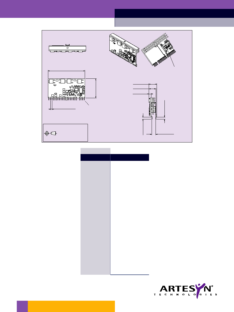
Figure 9: Mechanical Drawing and Pinout Table
Pin Connections
Pin No.
Function
1
TRIM
2
Not Connected
3
Ground
4
POWER GOOD
5
No Pin
6
Not Connected
7
Ground
8
Ground
9
Remote ON/OFF
10
Remote Sense (GND)
11
Remote Sense (O/P)
12
Vin
13
Vin
14
Vin
15
Vout
16
Vout
17
Ground
18
Vout
19
Ground
20
Vout
21
Ground
22
Vout
23
Ground
24
Vout

Note 1
Thermal reference point is defined as the highest temperature
measured at any one of the specified thermal reference points.
Note 2
The control pin is referenced to Vin-
Note 3
The SIL25C is supplied as standard with active High logic.
Control input pulled low: Unit Disabled
Control input left open: Unit Enabled
Note 4
Thermal reference set up: Unit mounted on an edge card test
board 215mm x 115mm. Test board mounted vertically. For test
details and recommended set-up see Application Note 1
48.
Note 5
3-200Hz, sweep at 1/2 octave/min from low to high frequency,
and then from high to low. Thirty minute dwell at all resonant
points.
CAUTION: Hazardous internal voltages and high temperatures.
Ensure that unit is accessible only to trained personnel. The user
must provide the recommended fusing in order to comply with
safety approvals.
SIL25C Series | 25 A DC-DC Converter
C Class Non-Isolated
18
10
www.artesyn.com
File Name: lf_sil25c_12_neg.pdf Rev (02): 22 Dec 2005

File Name: lf_sil25c_12_neg.pdf Rev (02): 22 Dec 2005
Longform Datasheet
© Artesyn TechnologiesÆ 2005
The information and specifications contained in this datasheet are
believed to be correct at time of publication. However, Artesyn
Technologies accepts no responsibility for consequences arising
from printing errors or inaccuracies. Specifications are subject to
change without notice. No rights under any patent accompany the
sale of any such product(s) or information contained herein.
N O R T H A M E R I C A
e-mail: sales.us@artesyn.com
§ 800 769 7274
§+508 628 5600
E U R O P E A N L O C A T I O N S
e-mail: sales.europe@artesyn.com
I R E L A N D
§+353 24 93130
A U S T R I A
§+43 1 80150
F A R E A S T L O C A T I O N S
e-mail: sales.asia@artesyn.com
H O N G K O N G
§+852 2699 2868
11
www.artesyn.com
SIL25C Series | 25 A DC-DC Converter
C Class Non-Isolated