 | ÐлекÑÑоннÑй компоненÑ: AS8E512K8 | СкаÑаÑÑ:  PDF PDF  ZIP ZIP |
Äîêóìåíòàöèÿ è îïèñàíèÿ www.docs.chipfind.ru
AS8E512K8
Rev. 2.0 12/99
Austin Semiconductor, Inc. reserves the right to change products or specifications without notice.
1
EEPROM
AS8E512K8
Austin Semiconductor, Inc.
GENERAL DESCRIPTION
The Austin Semiconductor, Inc. AS8E512K8 is a
4 Megabit CMOS EEPROM Module organized as 512K x 8-bits.
It is built with four 128K x 8 components and a single decoder.
The AS8E512K8 achieves high speed access, low power
consumption and high reliability by employing advanced CMOS
memory technology. Software data protection is implemented
using the JEDEC Optional Standard algorithm.
This military temperature grade product is ideally suited
for military and space applications requiring high reliability.
AVAILABLE AS MILITARY
SPECIFICATIONS
·
SMD 5962-93091
·
MIL-STD-883
FEATURES
·
Access times of 150, 200, 250, and 300 ns
·
JEDEC Compatible Pinout
·
10,000 Write Endurance Cycles
·
10 year Data Retention
·
Organized as 512Kx8
·
Operation with single 5 volt supply
·
Low power CMOS
·
TTL Compatible Inputs and Outputs
OPTIONS
MARKING
·
Packaging
32 pin 600 MIL DIP
CW No. 112
·
Timing
150ns
-150
200ns
-200
250ns
-250
300ns
-300
·
Operating Temperature Range
-Military (-55
o
C to +125
o
C)
XT
-Industrial (-40
o
C to +85
o
C)
IT
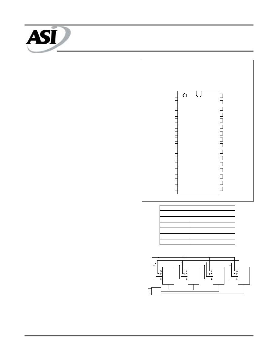
512K x 8 EEPROM
EEPROM Module
PIN ASSIGNMENT
(Top View)
32-Pin DIP & 32-Pin SOJ (CW)
A17
A18
CE\
I/O 0 - I/O 7
OE\
1 of 4
Decoder
U1
U4
U2
U3
I/O 0 - I/O 7
I/O 0 - I/O 7
I/O 0 - I/O 7
I/O 0 - I/O 7
A0 - A16
A0 - A16
A0 - A16
WE\
A0 - A16
WE\
WE\
WE\
OE\
OE\
OE\
CE\
A0 - A16
CE\
CE\
CE\
WE\
OE\
A18
A16
A15
A12
A7
A6
A5
A4
A3
A2
A1
A0
I/O 0
I/O 1
I/O 2
Vss
1
2
3
4
5
6
7
8
9
10
11
12
13
14
15
16
32
31
30
29
28
27
26
25
24
23
22
21
20
19
18
17
Vcc
WE\
A17
A14
A13
A8
A9
A11
OE\
A10
CE\
I/O 7
I/O 6
I/O 5
I/O 4
I/O 3
For more products and information
please visit our web site at
www.austinsemiconductor.com
A0 - A18
Address Inputs
I/O 0 - I/O 7
Data Inputs/Outputs
CE\
Chip Select
OE\
Output Enable
WE\
Write Enable
Vcc
+5.0V Power
PIN DESCRIPTION

AS8E512K8
Rev. 2.0 12/99
Austin Semiconductor, Inc. reserves the right to change products or specifications without notice.
2
EEPROM
AS8E512K8
Austin Semiconductor, Inc.
TOGGLE BIT:
In addition to DATA\ Polling the AS8E512K8 provides another
method for determining the end of a write cycle. During the write
operation, successive attempts to read data from the device will result
in I/O 6 toggling between one and zero. Once the write has completed,
I/O 6 will stop toggling and valid data will be read. Reading the toggle
bit may begin at any time during the write cycle.
DATA PROTECTION:
If precautions are not taken, inadvertent writes may occur during
transitions of the host power supply. The E
2
module has incorpo-
rated both hardware and software features that will protect the memory
against inadvertent writes.
HARDWARE PROTECTION:
Hardware features protect against inadvertent writes to the
AS8E512K8 in the following ways: (a) Vcc sense - if Vcc is below
3.8V (typical) the write function is inhibited; (b) Vcc power-on delay
- once Vcc has reached 3.8V the device will automatically time out
5ms (typical) before allowing a write; (c) write inhibit - holding any
one of OE\ low, CE\ high or WE\ high inhibits write cycles; (d) noise
filter - pulses of less than 15 ns (typical) on the WE\ or CE\ inputs will
not initiate a write cycle.
SOFTWARE DATA PROTECTION:
A software controlled data protection feature has been imple-
mented on theAS8E512K8. When enabled, the software data protec-
tion (SDP), will prevent inadvertent writes. The SDP feature may be
enabled or disabled by the user and is shipped with SDP disabled,
SDP is enabled by the host system issuing a series of three write
commands; three specific bytes of data are written to three specific
addresses (refer to Software Data Protection Algorithm). After
writing the three byte command sequence and after t
WC
the entire
AS8E512K8 will be protected from inadvertent write operations. It
should be noted, that once protected the host may still perform a byte
of page write to the AS8E512K8. This is done by preceding the data
to be written by the same three byte command sequence used to
enable SDP. Once set, SDP will remain active unless the disable
command sequence is issued. Power transitions do not disable SDP
and SDP will protect the AS8E512K8 during power-up and power-
down conditions. All command sequences must conform to the page
write timing specifications. The data in the enable and disable
command sequences is not written to the device and the memory
addresses used in the sequence may be written with data in either a
byte or page write operation.
After setting SDP, any attempt to write to the device without the
three byte command sequence will start the internal write timers. No
data will be written to the device; however, for the duration of t
WC
,
read operations will effectively be polling operations.
DEVICE OPERATION:
The AS8E512K8 is an electricaly erasable and programmable memory
module that is accessed like a Static RAM for the read or write cycle
without the need for external components. The device contains a
128-byte-page register to allow writing of up to 128 bytes of data
simultaneously. During a write cycle, the address and 1 to 128 bytes
of data are internally latched, freeing the address and data bus for other
operations. Following the initiation of a write cycle, the device will
automatically write the latched data using an internal control timer.
The end of a write cycle can be detected by DATA\ polling of I/O7.
Once the end of a write cycle has been detected a new access for a read
or write can begin.
READ:
The AS8E512K8 is accessed like a Static RAM. When C/E\ and
OE\ are low and WE\ is high, the data stored at the memory location
determined by the address pins is asserted on the outputs. The
outputs are put in the high impedance state when either CE\ or OE\ is
high. This dual-line control gives designers flexibility in preventing
bus contention in their system.
BYTE WRITE:
A low pulse on the WE\ or CE\ input with CE\ or WE\ low
(respectively) and OE\ high initiates a write cycle. The address is
latched on the falling edge of CE\ or WE\, whichever occurs last. The
data is latched by the first rising edge of CE\ or WE\. Once a byte,
word or double word write has been started it will automatically time
itself to completion.
PAGE WRITE:
The page write operation of the AS8E512K8 allows 1 to 128
BWDWs of data to be written into the device during a single internal
programming period. Each new BWDW must be written within 150us
(t
BLC
) of the previous BWDW. If the t
BLC
limit is exceeded the
AS8E512K8 will cease accepting data and commence the internal
programming operation. For each WE\ high to low transition during
the page write operation, A7-A18 must be the same.
The A0-A6 inputs are used to specify which bytes within the page
are to be written. The bytes may be loaded in any order and may be
altered within the same load period. Only bytes which are specified
for writing will be written; unnecessary cycling of other bytes within
the page does not occur.
DATA\ POLLING:
The AS8E512K8 features DATA\ Polling to indicate the end of a
write cycle. During a byte or page write cycle an attempted read of
the last byte written will result in the complement of the written data
to be presented on I/O 7. Once the write cycle has been completed,
true data is valid on all outputs, and the next write cycle may begin.
DATA\ Polling may begin at anytime during the write cycle.
AS8E512K8
Rev. 2.0 12/99
Austin Semiconductor, Inc. reserves the right to change products or specifications without notice.
3
EEPROM
AS8E512K8
Austin Semiconductor, Inc.
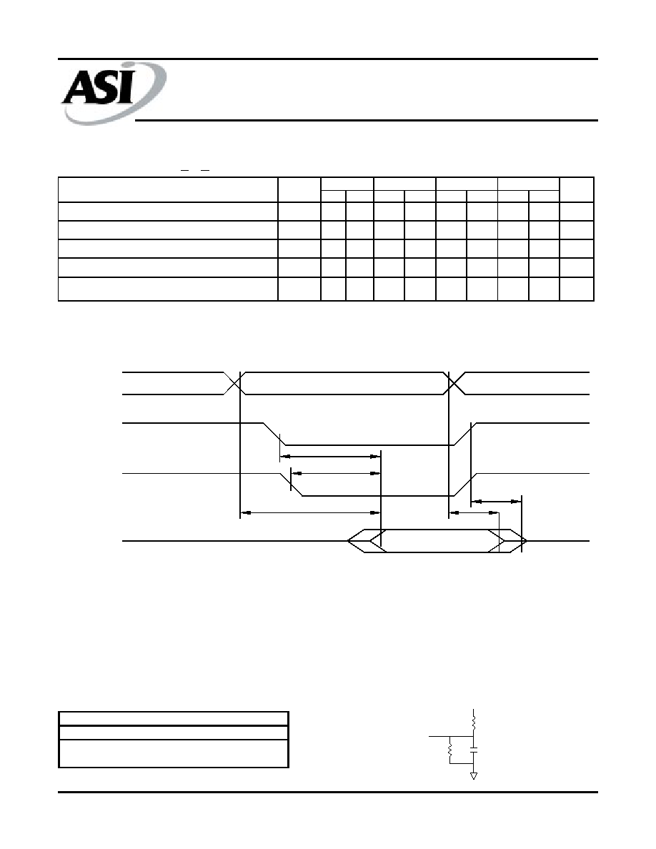
PIN CAPACITANCE (f= 1MHz, T = 25° C)
(1)
ELECTRICAL CHARACTERISTICS AND RECOMMENDED DC OPERATING CONDITIONS
(-55
o
C<T
A
<+125
o
C; Vcc = 5V +10%)
OPERATING MODES
ABSOLUTE MAXIMUM RATINGS*
Voltage on Vcc Supply Relative to Vss
Supply/Input Voltage Range
1
.........................-0.6V to +6.25V DC
Voltage on OE\ and A9....................................-0.6V to +13.5V DC
Voltage on all other pins..................................-0.6V to +6.25V DC
Storage Temperature.............................................-65
°
C to +150
°
C
Operating Temperature, T
A
(Ambient)................-55
o
C to +125
o
C
Lead Temperature (soldering 10 seconds)........................+300
o
C
Maximum Junction Temperature**....................................+165
°
C
NOTE:
1. Including NC pins, with respect to ground.
*Stresses greater than those listed under "Absolute Maximum
Ratings" may cause permanent damage to the device. This is
a stress rating only and functional operation of the device at
these or any other conditions above those indicated in the
operation section of this specification is not implied. Exposure
to absolute maximum rating conditions for extended periods
may affect reliability.
** Junction temperature depends upon package type, cycle
time, loading, ambient temperature and airflow.
NOTE:
1. X can be V
IL
or V
IH.
2. Refer to AC Programming Waveforms.
SYMBOL
CONDITIONS
MAX
UNIT
C
ADD, OE\, WE\
V
IN
= 0V, f = 1MHz
45
pF
C
I/O
V
OUT
= 0V, f = 1MHz
50
pF
C
CE\
V
IN
= 0V, f = 1MHz
10
pF
MODE
CE\
OE\
WE\
I/O
Read
V
IL
V
IL
V
IH
D
OUT
Write
2
V
IL
V
IH
V
IL
D
IN
Standby/Write Inhibit
V
IH
X
1
X
High Z
Write Inhibit
X
X
V
IH
Write Inhibit
X
V
IL
X
Output Disable
X
V
IH
X
High Z
PARAMETER
CONDITION
SYMBOL
MIN
MAX
UNITS
Input Load Current
V
IN
= OV to Vcc + 1V
I
LI
-20
20
µ
Output Leakage Current
V
I/O
= OV to Vcc
I
LO
-20
20
µ
Vcc Standby Current CMOS
CE\ = Vcc -0.2V to Vcc + 1
I
SB1
mA
Vcc Standby Current TTL
CE\ = 2.2V to Vcc + 1
I
SB2
20
mA
Vcc Active Current
F = 5 MHz; I
OUT
= 0 mA
I
CC
120
mA
Input Low Voltage
V
IL
0.8
V
Input High Voltage
V
IH
2
V
Output Low Voltage
I
OL
= 2.1 mA
V
OL
0.45
V
Output High Voltage
I
OH
= -400
µ
A
V
OH1
2.4
V
Output High Voltage CMOS
I
OH
= -100
µ
A; Vcc = 4.5V
V
OH2
4.2
V
AS8E512K8
Rev. 2.0 12/99
Austin Semiconductor, Inc. reserves the right to change products or specifications without notice.
4
EEPROM
AS8E512K8
Austin Semiconductor, Inc.
A.C. READ WAVEFORMS
(1,2,3,4)
NOTES:
1. CE\ may be delayed up to t
ACC
-t
CE
after the address transi-
tion without inpact on t
ACC
.
2. OE\ may be delayed up to t
CE
-t
OE
after the falling edge of
CE\ without inpact on t
CE
or by t
ACC
-t
OE
after an address
change without inpact on t
ACC
.
3. t
DF
is specified from OE\ or CE\ whichever occurs first
(C
L
= 5pF).
4. This parameter is characterized and is not 100% tested.
5. A17 and A18 must remain valid through the WE\ and CE\
low pulse.
ELECTRICAL CHARACTERISTICS AND RECOMMENDED AC READ OPERATING
CONDITIONS (-55
o
C<T
A
<+125
o
C; Vcc = 5V +10%)
INPUT TEST WAVEFORMS AND MEASUREMENT
LEVEL FOR AC TEST CONDITIONS
In p u t P u ls e L e v e ls
0 V to 3 .0 V
In p u t R is e a n d F a ll T im e s
5 n S
In p u t a n d O u tp u t
1 .5 V
T im in g R e fe re n c e L e v e ls
OUTPUT TEST LOAD
100pF
1.8K
1.3K
5.0V
ADDRESS
CE\
OE\
OUTPUT
OUTPUT
HIGH Z
t
OE
t
ACC
t
DF
t
CE
ADDRESS VALID
t
OH
VALID
�
�
�
��
�
��
�
�
�
�
�
�
!" # ""
!
�
�
�
�
�
AS8E512K8
Rev. 2.0 12/99
Austin Semiconductor, Inc. reserves the right to change products or specifications without notice.
5
EEPROM
AS8E512K8
Austin Semiconductor, Inc.
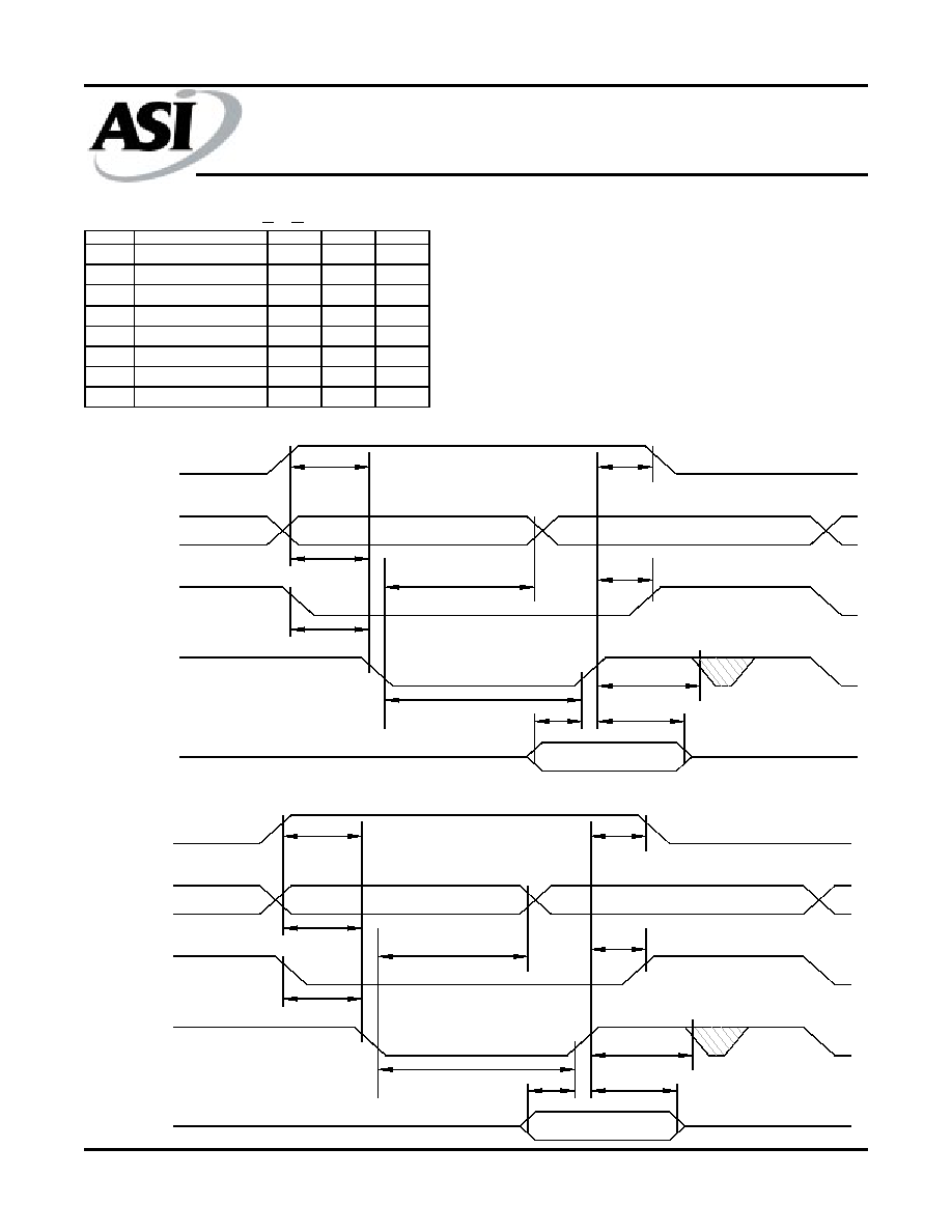
AC WRITE WAVEFORMS - CE\ CONTROLLED
5
AC WRITE WAVEFORMS - WE\ CONTROLLED
5
ELECTRICAL CHARACTERISTICS AND RECOMMENDED AC WRITE OPERATING
CONDITIONS (-55
o
C<T
A
<+125
o
C; Vcc = 5V +10%)
OE\
ADDRESS
CE\
WE\
DATA IN
t
OES
t
AS
5
t
AH
5
t
CS
t
WP
t
DS
t
OEH
t
CH
t
WPH
t
DH
SYMBOL
PARAMETER
MIN
MAX
UNITS
t
WC
Write Cycle Time
10
ms
t
AS
Address Set-up time
10
ns
t
AH
Address Hold Time
5
50
ns
t
DS
Data Set-up Time
50
ns
t
DH
Data Hold Time
0
ns
t
WP
Write Pulse Width
100
ns
t
BLC
Byte Load Cycle Time
150
µ
s
t
WPH
Write Pulse Width High
50
ns
OE\
ADDRESS
DATA IN
t
OES
t
AS
5
t
AH
5
t
CS
t
WP
t
DS
t
OEH
t
CH
t
WPH
t
DH
?WE\
CE\