 | –≠–ª–µ–∫—Ç—Ä–æ–Ω–Ω—ã–π –∫–æ–º–ø–æ–Ω–µ–Ω—Ç: 65554 | –°–∫–∞—á–∞—Ç—å:  PDF PDF  ZIP ZIP |
Document Outline
- Exit
- Front Page
- 65554 Intro/Features
- System Diagrams
- Figure 1: System Diagram - External Interfaces
- Figure 2: System Diagram - Internal Data Flow
- 6555x Software Support Features
- Revision History
- TABLE OF CONTENTS
- TABLE OF FIGURES
- LIST OF TABLES
- Chapter 1 Introduction/Overview
- 1. Introduction / Overview
- 1.1 High Performance
- 1.2 Hardware Multimedia Support
- 1.3 Versatile Panel Support
- 1.4 Low Power Consumption
- 1.5 Software Compatibility / Flexibility
- 1.6 Display Memory Size Requirements
- Figure 1-1: Display Memory Configurations
- Figure 1-2: Display Memory Configurations with an STN-DD Buffer
- Chapter 2 Pin Descriptions
- 2.0 PIN DESCRIPTIONS
- 2.1 Top View: BGA Ball Assignments
- Figure 2-1: Pin Diagram
- 2.2 Bottom View: BGA Ball Assignments
- Figure 2-2: Pin Diagram
- 2.3 PCI BUS INTERFACE
- 2.4 DISPLAY MEMORY INTERFACE
- 2.5 FLAT PANEL DISPLAY INTERFACE
- 2.6 CRT INTERFACE
- 2.7 POWER / GROUND AND STANDBY CONTROL
- 2.8 VIDEO INTERFACE
- 2.9 MISCELLANEOUS
- Chapter 3 I/O and Memory Address Maps
- 3.0 INTRODUCTION
- 3.1 I/O Map
- 3.2 Sub-Addressing Indexes and Data Ports
- 3.3 Memory Map
- 3.4 PCI Configuration Registers
- Chapter 4 Register Summaries
- 4.0 REGISTER SUMMARIES
- 4.1 Sequencer Registers
- 4.2 Graphics Controller Registers
- 4.3 Attribute Controller Registers
- 4.4 VGA Color Palette Registers
- 4.5 CRT Controller Registers
- 4.6 PCI Configuration Registers
- 4.7 BitBLT Registers
- 4.8 Extension Registers
- 4.9 Multimedia Registers
- 4.10 Flat Panel Registers
- Chapter 5 General Control and Status Register Descriptions
- 5.0 GENERAL CONTROL AND STATUS REGISTERS
- ST00 Input Status Register 0
- ST01 Input Status Register 1
- FCR Feature Control Register
- MSR Miscellaneous Output Register
- Chapter 6 Sequencer Registers
- 6.0 SEQUENCER REGISTERS
- SRX Sequencer Index Register
- SR00 Reset Register
- SR01 Clocking Mode Register
- SR02 Plane Mask Register
- SR03 Character Map Select Register
- SR04 Memory Mode Register
- SR07 Horizontal Character Counter Reset
- Chapter 7 Graphics Controller Registers
- 7.0 GRAPHICS CONTROLLER REGISTERS
- GRX Graphics Controller Index Register
- GR00 Set/Reset Register
- GR01 Enable Set/Reset Register
- GR02 Color Compare Register
- GR03 Data Rotate Register
- GR04 Read Plane Select Register
- GR05 Graphics Mode Register
- GR06 Miscellaneous Register
- GR07 Color Donêt Care Register
- GR08 Bit Mask Register
- Chapter 8 Attribute Controller Registers
- 8.0 ATTRIBUTE CONTROLLER REGISTERS
- ARX Attribute Controller Index Register
- AR00-AR0F Palette Registers 0-F
- AR10 Mode Control Register
- AR11 Overscan Color Register
- AR12 Memory Plane Enable Register
- AR13 Horizontal Pixel Panning Register
- AR14 Color Select Register
- Chapter 9 Palette DAC Registers
- 9.0 PALETTE DAC REGISTERS
- DACMASK Pixel Data Mask Register
- DACSTATE DAC State Register
- DACRX Palette Read Index Register
- DACWX Palette Write Index Register
- DACDATA Palette Data Register
- Chapter 10 CRT Controller Registers
- 10 CRT CONTROLLER REGISTERS
- CRX CRT Controller Index Register
- CR00 Horizontal Total Register
- CR01 Horizontal Display Enable End Register
- CR02 Horizontal Blanking Start Register
- CR03 Horizontal Blanking End Register
- CR04 Horizontal Sync Start Register
- CR05 Horizontal Sync End Register
- CR06 Vertical Total Register
- CR07 Overflow Register
- CR08 Preset Row Scan Register
- CR09 Maximum Scan Line Register
- CR0A Text Cursor Start Register
- CR0B Text Cursor End Register
- CR0C Start Address High Register
- CR0D Start Address Low Register
- CR0E Text Cursor Location High Register
- CR0F Text Cursor Location Low Register
- CR10 Vertical Sync Start Register
- CR11 Vertical Sync End Register
- CR12 Vertical Display Enable End Register
- CR13 Offset Register
- CR14 Underline Location Register
- CR15 Vertical Blanking Start Register
- CR16 Vertical Blanking End Register
- CR17 CRT Mode Control
- CR18 Line Compare Register
- CR22 Memory Read Latch Data Register
- CR30 Extended Vertical Total Register
- CR31 Extended Vertical Display End Register
- CR32 Extended Vertical Sync Start Register
- CR33 Extended Vertical Blanking Start Register
- CR40 Extended Start Address Register
- CR41 Extended Offset Register
- CR70 Interlace Control Register
- CR71 NTSC/PAL Video Output Control Register
- CR72 Horizontal Serration 1 Start Register
- CR73 Horizontal Serration 2 Start Register
- CR74 NTSC/PAL Horizontal Pulse Width Register
- Chapter 11 PCI Configuration Registers
- 11.0 PCI CONFIGURATION REGISTERS
- VENDID Vendor ID
- DEVID Device ID
- DEVCTL Device Control
- DEVSTAT Device Status
- REV Revision
- PRG Register-Level Programming Interface
- SUB Sub-Class Code
- BASE Base Class Code
- HDR Header Type
- MBASE Memory Base Address
- RBASE ROM Base Address
- Chapter 12 BitBLT Registers
- 12.0 BITBLT REGISTERS
- BR00 Source and Destination Offset Register
- BR01 Pattern/Source Expansion Background Color Register
- BR02 Pattern/Source Expansion Foreground Color Register
- BR03 Monochrome Source Control Register
- BR04 BitBlt Control Register
- BR05 Pattern Address Register
- BR06 Source Address Register
- BR07 Destination Address Register
- BR08 Destination Width & Height Register
- BR09 Source Expansion Background Color Register
- BR0A Source Expansion Foreground Color Register
- Chapter 13 Extension Registers
- 13.0 EXTENSION REGISTERS
- 13.1 BASIC SYSTEM CONFIGURATION
- XR00 Vendor ID Low
- XR01 Vendor ID High
- XR02 Device ID Low
- XR03 Device ID High
- XR04 Revision ID
- XR05 Linear Base Address Low
- XR06 Linear Base Address High
- XR08 Configuration
- XR09 I/O Control
- XR0A Address Mapping
- XR0B Burst Write mode
- XR0E Page Selector
- 13.2 BitBLT ENGINE CONTROL REGISTER
- XR20 BitBLT Configuration Control
- 13.3 MEMORY CONFIGURATION
- XR40 DRAM Access Control Register
- XR41 DRAM Type Register
- XR42 DRAM Configuration Register
- XR43 DRAM Interface
- XR44 DRAM Timing Register
- 13.4 PIN CONTROL REGISTERS
- XR60 Video Pin Control
- XR61 DDC Sync Select
- XR62 GPIO Control
- XR63 GPIO Data
- XR67 Pin Tri-State Control
- XR70 Configuration Pin 0 Register
- XR71 Configuration Pin 1 Register
- 13.5 PIXEL PIEPLINE CONTROL
- XR80 Pixel Pipeline Configuration 0
- XR81 Pixel Pipeline Configuration 1
- XR82 Pixel Pipeline Configuration 2
- 13.6 HARDWARE CURSOR 1 & 2
- XRA0 Cursor 1 Control Register
- XRA1 Cursor 1 Vertical Extension Register
- XRA2 Cursor 1 Base Address Low Register
- XRA3 Cursor 1 Base Address High Register
- XRA4 Cursor 1 X-Position Low Register
- XRA5 Cursor 1 X-Position High Register
- XRA6 Cursor 1 Y-Position Low Register
- XRA7 Cursor 1 Y-Position High Register
- XRA8 Cursor 2 Control Register
- XRA9 Cursor 2 Vertical Extension Register
- XRAA Cursor 2 Base Address Low Register
- XRAB Cursor 2 Base Address High Register
- XRAC Cursor 2 X-Position Low Register
- XRAD Cursor 2 X-Position High Register
- XRAE Cursor 2 Y-Position Low Register
- XRAF Cursor 2 Y-Position High Register
- 13.7 CLOCK CONTROL
- XRC0 Video Clock 0 VCO M-Divisor
- XRC1 Video Clock 0 VCO N-Divisor
- XRC2 Video Clock 0 VCO M/N-Divisor MSBs
- XRC3 Video Clock 0 Divisor Select
- XRC4 Video Clock 1 VCO M-Divisor
- XRC5 Video Clock 1 VCO N-Divisor
- XRC6 Video Clock 1 VCO M/N-Divisor MSBs
- XRC7 Video Clock 1 Divisor Select
- XRC8 Video Clock 2 VCO M-Divisor
- XRC9 Video Clock 2 VCO N-Divisor
- XRCA Video Clock 2 VCO M/N-Divisor MSBs
- XRCB Video Clock 2 Divisor Select
- XRCC Memory Clock VCO M-Divisor
- XRCD Memory Clock VCO N-Divisor
- XRCE Memory Clock Divisor Select
- XRCF Clock Configuration
- 13.8 POWER MANAGEMENT
- XRD0 Module PowerDown 0
- XRD2 Down Counter
- XRE0ÖXRE7 Software Flags x
- XRF8-XRFC Test Registers
- Chapter 14 Multimedia Registers
- 14.0 MULTIMEDIA REGISTERS
- MR00 Module Capability
- MR01 Secondary Capability
- 14.1 ACQUISITION CONTROL
- MR02 Acquisition Control 1
- MR03 Acquisition Control 2
- MR04 Acquisition Control 3
- MR05 Acquisition Control 4
- MR06 Acquisition Memory Address PTR1
- MR07 Acquisition Memory Address PTR1
- MR08 Acquisition Memory Address PTR1
- MR09 Acquisition Memory Address PTR2
- MR0A Acquisition Memory Address PTR2
- MR0B Acquisition Memory Address PTR2
- MR0C Acquisition Memory Width (Span)
- MR0E Acquisition Window XLEFT
- MR0F Acquisition Window XLEFT
- MR10 Acquisition Window XRIGHT
- MR11 Acquisition Window XRIGHT
- MR12 Acquisition Window Y-TOP
- MR13 Acquisition Window Y-TOP
- MR14 Acquisition AQ Window Y-BOTTOM
- MR15 Acquisition Window Y-BOTTOM
- MR16 H-SCALE
- MR17 V-SCALE
- MR18 Capture Frame Count
- 14.2 PLAYBACK CONTROL
- MR1E Display Control 1
- MR1F Display Control 2
- MR20 Display Control 3
- MR21 Double Buffer Status
- MR22 Playback Memory Address PTR1
- MR23 Playback Window Address PTR1
- MR24 Playback Memory Address PTR1
- MR25 Playback Memory Address PTR2
- MR26 Playback Memory Address PTR2
- MR27 Playback Memory Address PTR2
- MR28 Playback Memory Width (Span)
- MR2A Playback Window XLEFT
- MR2B Playback Window XLEFT
- MR2C Playback Window
- MR2D Playback Window XRIGHT
- MR2E Playback Window Y-TOP
- MR2F Playback Window Y-TOP
- MR30 Playback Window Y-BOTTOM
- MR31 Playback Window Y-BOTTOM
- MR32 H-ZOOM
- MR33 V-ZOOM
- MR3C Color Key Control 1
- MR3D-3F Color Keys
- MR40-42 Color Key Masks
- MR43 Line Count
- MR44 Line Count
- Chapter 15 Flat Panel Registers
- 15.0 FLAT PANEL REGISTERS
- FR00 Feature Register
- FR01 CRT / FP Control
- FR02 FP Mode Control
- FR03 FP Dot Clock Source
- FR04 Panel Power Sequencing Delay
- FR05 Power Down Control 1
- FR06 FP Power Down Control
- FR08 FP Pin Polarity
- FR0A Programmable Output Drive
- FR0B FP Pin Control 1
- FR0C Pin Control 2
- FR0F Activity Timer Control
- FR10 FP Format 0
- FR11 FP Format 1
- FR12 FP Format 2
- FR13 FP Format 3
- FR16 FRC Option Select
- FR17 Polynomial FRC Control
- FR18 FP Text Mode Control
- FR19 Blink Rate Control
- FR1A Frame Buffer Control
- FR1E M (ACDCLK) Control
- FR1F Diagnostic
- FR20 FP Horizontal Panel Display Size LSB
- FR21 FP Horizontal Sync Start LSB
- FR22 FP Horizontal Sync End
- FR23 FP Horizontal Total LSB
- FR24 FP HSync (LP) Delay LSB
- FR25 FP Horizontal Overflow 1
- FR26 FP Horizontal Overflow 2
- FR27 FP HSync (LP) Width and Disable
- FR30 FP Vertical Panel Size LSB
- FR31 FP Vertical Sync Start LSB (FR31)
- FR32 FP Vertical Sync End
- FR33 FP Vertical Total LSB
- FR34 FP VSync (FLM) Delay LSB
- FR35 FP Vertical Overflow 1
- FR36 FP Vertical Overflow 2
- FR37 FP VSync (FLM) Disable
- FR40 Horizontal Compensation Register
- FR41 Horizontal Stretching Register
- FR48 Vertical Compensation Register
- FR49-4C Text Mode Vertical Stretching 0 MSB
- FR4D Vertical Line Replication Register
- FR4E Selective Vertical Stretching Disable Register
- Chapter 16 Electrical Specifications
- 16 ELECTRICAL SPECIFICATIONS
- Table 16-1: 65554 Absolute Maximum Conditions
- Table 16-2: 65554 Normal Operating Conditions
- Table 16-3: 65554 DAC Characteristics:
- Table 16- 4: 65554 DC Characteristics:
- Table 16- 5: 65554 DC Drive Characteristics
- Table 16- 6: 65554 AC Test Conditions:
- Figure 16-1: AC Test Timing
- Table 16- 7: 65554 AC Timing Characteristics - Reference Clock
- Figure 16-2: Reference Clock Timing
- Table 16- 8: 65554 AC Timing Characteristics - Clock Generator
- Table 16- 9: 65554 AC Timing Characteristics - Reset
- Figure 16-3: Reset Timing
- Table 16- 10: 65554 AC Timing Characteristics - PCI Bus Frame (CLK=33MHz)
- Figure 16-4: PCI Bus Frame Timing
- Table 16- 11: 65554 AC Timing Characteristics - PCI Bus Stop (CLK=33MHz)
- Figure 16-5: PCI Bus Stop Timing
- Table 16- 12: 65554 AC Timing Characteristics PC BIOS ROM
- Figure 16-6: PCI BIOS ROM Timing
- Table 16- 13: 65554 AC Timing Characteristics - DRAM Read / Write
- Figure 16-7: DRAM Read Cycle Timing
- Figure 16-8: DRAM Write Cycle Timing
- Table 16-14: 65554 AC Timing Characteristics - CBR Refresh
- Figure 16-9: CAS-Before-RAS (CBR) DRAM Refresh Cycle Timing
- Table 16-15: 65554 AC Timing Characteristics - Self Refresh
- Figure 16-10: çSelf Refresh DRAMé Refresh Cycle Timing
- Table 16- 16: 65554 AC Timing Characteristics - Video Input Port
- Figure 16-11: Video Data Port Timing
- Table 16- 7: 65554 AC Timing Characteristics - Panel Output Timing
- Figure 16-2: Panel Output Timing
- Chapter 17 Mechanical Specifications
- 17 MECHANICAL SPECIFICATIONS
- Appendix A Clock Generation
- A. Clock Generation
- A.1 Clock Synthesizer
- A.2 Dot Clock (DCLK)
- A.3 Memory Clock (MCLK)
- A.4 PLL Parameters
- A.5 Programming the Clock Synthesizer
- A.6 DCLK Programming
- A.7 MCLK Programming
- A.8 Programming Constraints
- A.9 Programming Example
- A.10 Display Memory Bandwidth
- A.11 STN-DD Panel Buffering
- A.12 Horizontal and Vertical Clocking
- Appendix B VGA Standard Modes
- Appendix C Panel Power Sequencing
- C. Panel Power Sequencing
- Appendix D Hardware Curose and Pop Up Window
- D HARDWARE CURSOR AND POP UP WINDOW
- D.1 Cursor Configuration
- D.1.1 Basic Cursor Configuration
- D.1.2 Base Address for Cursor Data
- D.1.3 Cursor Vertical Extension
- D.1.4 Cursor Colors
- D.2. Cursor Modes
- D.2.1 32x32x2bpp & 64x64x2bpp AND/XOR Pixel Plane Modes
- Table D-1: Memory Organization
- Table D-2: Memory Organization
- Table D-3: Pixel Data 32x32x2bpp
- D.2.2 64x64x2bpp 4-Color Mode
- Table D-4: Memory Organization
- Table D-5: Pixel Data
- D.2.3 64x64x2bpp 3-Color and Transparency Mode
- Table D-6: Memory Organization
- Table D-7: Pixel Data
- D.2.4 128x128x1bpp 2-Color Mode
- Table D-8: Memory Organization
- Table D-9: Pixel Data
- D.2.5 The 128x128x1bpp 1-Color and Transparency Mode
- Table D-10: Memory Organization
- Table D-11: Pixel Bit Definitions
- D.3 Cursor Positioning
- Appendix E BitBLT Engine
- E. HiQVideo(tm) Series BitBLT Engine
- E.1 Introduction
- Figure E-1: Block Diagram and Data Paths of the BitBLT Engine
- E.2 Basic BitBLT Functional Considerations
- E.2.1 Color Depth Configuration and Color Expansion
- E.2.2 Graphics Data Size Limitations
- E.2.3 Bit-Wise Operations
- Table E-1: Bit-Wise Operations and 8-bit Codes (00 - 3F)
- Table E-2: Bit-Wise Operations and 8-bit Codes (40 - 7F)
- Table E-3: Bit-Wise Operations and 8-bit Codes (80 - BF)
- Table E-4: Bit-Wise Operations and 8-bit Codes (C0 - FF)
- E.2.4 Per-Pixel Write-Masking Operations
- Figure E-2: Block Diagram and Data Paths of the BitBLT Engine
- E.2.5 When the Source and Destination Locations Overlap
- Figure E-2-1: Source Corruption in BitBLT with Overlapping Source and Destination Locations
- Figure E-2-2: Correctly Performed BitBLT with Overlapping Source and Destination Locations
- Figure E-2-3: Suggested Starting Points for Possible Source and Destination Overlap Situations
- E.3 Basic Graphics Data Considerations
- E.3.1 Contiguous vs. Discontiguous Graphics Data
- Figure E-3-1: Representation of On-Screen Single 6-Pixel Line in the Frame Buffer
- Figure E-3-2: Representation of On-Screen 6x4 Array of Pixels in the Frame Buffer
- E.3.2 Source Data
- E.3.3 Monochrome Source Data
- E.3.4 Pattern Data
- Figure E-3-3: Pattern Data -- Always an 8x8 Array of Pixels
- Figure E-3-4: Monochrome Pattern Data -- Occupies a Single Quadword
- Figure E-3-5: 8bpp Pattern Data -- Occupies 64 Bytes (8 Quadwords)
- Figure E-3-6: 16bpp Pattern Data -- Occupies 128 Bytes (16 Quadwords)
- Figure E-3-7: 24bpp Pattern Data -- Occupies 256 Bytes (32 Quadwords)
- E.3.5 Destination Data
- E.4. BitBLT Programming Examples
- E.4.1 Pattern Fill -- A Very Simple BitBLT
- Figure E-4-1: On-Screen Destination for Example Pattern Fill BitBLT
- Figure E-4-2: Pattern Data for Example Pattern Fill BitBLT
- Figure E-4-3: Results of Example Pattern Fill BitBLT
- E.4.2 Drawing Characters Using a Font Stored in System Memory
- Figure E-4-4: On-Screen Destination for Example Character Drawing BitBLT
- Figure E-4-5: Source Data in System Memory for Example Character Drawing BitBLT
- Figure E-4-6: Results of Example Character Drawing BitBLT
- Appendix F Memory Configurations
- F. Memory Configurations
- F.1 Introduction
- F.2 Memory Interface (32 or 64 Bit) with an External STN-DD Buffer
- F.3 Support for FPM and EDO DRAM Types
- F.4 Support for Dual-CAS or Dual-WE (per Word) DRAMs
- Table F-1 CAS and WE Signal Functions
- Table F-2 CAS and WE Signal Functions
- Table F-3 CAS and WE Signal Functions
- F.5 Memory Configuration Overview
- Table F-4: Depicted Memory Configurations
- F.5.1 1MB, 64-bit Memory Configuration Using Two 128Kx32 DRAMs
- Figure F-1: 1MB, 64-bit Memory Configuration Using Two 128Kx32 DRAMs
- F.5.2 1MB, 32-bit Memory Configuration Using Two 128Kx32 DRAMs
- Figure F-2: 1MB, 32-bit Memory Configuration Using Two 128Kx32 DRAMs
- F.5.3 2MB, 64-bit Memory Configuration Using Four 128Kx32 DRAMs
- Figure F-3: 2MB, 64-bit Memory Configuration Using Four 128Kx32 DRAMs
- F.5.4 1MB, 32-bit Memory Configuration Using Two 256Kx16 DRAMs
- Figure F-4: 1MB, 32-bit Memory Configuration Using Two 256Kx16 DRAMs
- F.5.5 2MB, 64-bit Memory Configuration Using Four 256Kx16 DRAMs
- Figure F-5: 2MB, 64-bit Memory Configuration Using 256Kx16 DRAMs
- F.5.6 4MB, 64-bit Memory Configuration Using Eight 256Kx16 DRAMs
- Figure F-6: 4MB, 64-bit Memory Configuration Using Eight 256Kx16 DRAMs
- F.5.7 2MB, 32-bit Memory Configuration Using a Single 512Kx32 DRAM
- Figure F-7: 2MB, 32-bit Memory Configuration Using a Single 512Kx32 DRAM
- F.5.8: 4MB, 64-bit Memory Configuration Using Two 512Kx32 DRAMs
- Figure F-8: 4MB, 64-bit Memory Configuration Using Two 512Kx32 DRAMs
- Back Page

65554
High Performance Flat Panel/
CRT GUI Accelerator
Data Sheet
Revision 1.5
October 1997
&+,36
Æ

Copyright Notice
Copyright
©
1997 Chips and Technologies, Inc. ALL RIGHTS RESERVED.
This manual is copyrighted by Chips and Technologies, Inc. You may not reproduce,
transmit, transcribe, store in a retrieval system, or translate into any language or computer
language, in any form or by any means - electronic, mechanical, magnetic, optical,
chemical, manual, or otherwise - any part of this publication without the express written
permission of Chips and Technologies, Inc.
Restricted Rights Legend
Use, duplication, or disclosure by the Government is subject to restrictions set forth in
subparagraph (c)(1)(ii) of the Rights in Technical Data and Computer Software clause at
252.277-7013.
Trademark Acknowledgment
CHIPS Logo, PEAK, PRINTGINE, SCAT, and WINGINE are registered trademarks of
Chips and Technologies, Inc.
HiQVideo, HiQV32, HiQV64, HiQV64P, HiQVPro, HiQVDual, HiQVDualP, HiQV-
MPEG, HiQV-3D, and "Solutions for a Changing World" are trademarks of Chips and
Technologies, Inc.
Brooktree and RAMDAC are trademarks of Brooktree Corporation.
Hercules is a trademark of Hercules Computer Technology.
Inmos is a trademark of Inmos Corporation.
386SX, i387, 486, i486, and Pentium are trademarks of Intel Corporation.
IBM, AT, PS/2, and Personal System/2 are registered trademarks of International Business
Machines Corporation. XT is a trademark of International Business Machines Corporation.
Microsoft is a registered trademark of Microsoft Corporation. MS-DOS and Windows are
trademarks of Microsoft Corporation.
TRI-STATE is a registered trademark of National Semiconductor Corporation.
MultiSync is a trademark of Nippon Electric Company (NEC).
PanelLink technology is licensed by Chips and Technologies, Inc. from Silicon Image, Inc.
Of Palo Alto, CA. PanelLink is a trademark of Silicon Image, Inc.
VESA is a registered trademark of Video Electronics Standards Association.
VL-Bus is a trademark of Video Electronics Standards Association.
Weitek is a registered trademark of Weitek Inc.
All other trademarks are the property of their respective holders.
Disclaimer
This document provides general information for the customer. Chips and Technologies, Inc., reserves the
right to modify the information contained herein as necessary and the customer should ensure that it has the
most recent revision of the document. CHIPS makes no warranty for the use of its products and bears no
responsibility for any errors which may appear in this document. The customer should be on notice that
many different parties hold patents on products, components, and processes within the personal computer
industry. Customers should ensure that their use of the products does not infringe upon any patents. CHIPS
respects the patent rights of third parties and shall not participate in direct or indirect patent infringement.

&+,36
Æ
I
NTRODUCTION
/ O
VERVIEW
R
EVISION
1.5
10/16/97
65554
S
UBJECT TO CHANGE WITHOUT NOTICE
65554 (HiQV64
TM
TM
)
High Performance MultiMedia Flat Panel / CRT
GUI Accelerator
s Highly integrated design Flat Panel and CRT GUI
Accelerator & Multimedia Engine, Palette/DAC,
and Clock Synthesizer
s Hardware Windows Acceleration
∑ 64-bit Graphics Engine
- System-to-Screen and
Screen-to-Screen BitBLT
- 3-Operand Raster-Ops
- 8/16/24 Color Expansion
∑ Transparent BLT
- Optimized for WindowsTM
BitBLT format
s PCI Bus with Burst Mode capability and BIOS
ROM support
s Flexible Memory Configurations
∑ 64-Bit memory interface
∑ Two, four, or eight 256Kx16 DRAMs
(1MB, 2MB, or 4MB)
∑ One or two 512Kx32 DRAMs (2MB or 4MB)
∑ Two 128Kx32 DRAMs (1MB)
∑ Four 128Kx16 DRAMs (1MB)
s High Performance:
∑ Deep write buffers
∑ EDO DRAM Support
-55 MHz @ 3.3V
s Hardware Multimedia Support
∑ Zoom Video port
∑ YUV input from System Bus or Video Port
∑ YUV-RGB Conversion
∑ Capture / Scaling
∑ Zoom up to 8x
∑ Interpolation
∑ Double Buffered Video
s Display centering and stretching features for
optimal fit of VGA graphics and text on 800x600
and 1024x768 panels
s Simultaneous Hardware Cursor and Pop-up Window
∑ 64x64 pixels by 4 colors
∑ 128x128 pixels by 2 colors
s Game Acceleration
∑ Source Transparent BLT
∑ Destination Transparent BLT
∑ Double buffer support for YUV and 15/16Bpp
Overlay Engine
∑ Instant Full Screen Page Flip
∑ Read back of CRT Scan line counters
s Optimized for High Performance Flat Panel
Display at 3.3V
∑ 640x480 x 24bpp
∑ 800x600 x 24bpp
∑ 1024x768 x 16bpp
s CRT Support
∑ 94.5 MHz @ 3.3V
s Direct interface to Color and Monochrome, Single
Drive (SS), and Dual Drive (DD), STN & TFT
panels
s Flexible On-chip Activity Timer facilitates ordered
shut-down of the display system
s Advanced Power Management feature minimizes
power usage in:
∑ Normal operation
∑ Standby (Sleep) modes
∑ Panel-Off Power-Saving Mode
s VESA Standards supported
∑ VAFC Port for display of "Live" Video
∑ DPMS for CRT power-down (required for
support of EPA Energy-Star program)
∑ DDC for CRT Plug-Play & Display Control
s Composite NTSC / PAL Support
s Power Sequencing control outputs regulate
application of Bias voltage, +5V to the panel and
+12V to the inverter for backlight operation
s 3.3V core and 3.3/5.0V I/O Operation
s Fully Compatible with IBM
Æ
VGA

&+,36
Æ
I
NTRODUCTION
/ O
VERVIEW
R
EVISION
1.5
10/16/97
65554
S
UBJECT TO CHANGE WITHOUT NOTICE
ii
This page intentionally left blank.
&+,36
Æ
I
NTRODUCTION
/ O
VERVIEW
R
EVISION
1.5
10/16/97
65554
S
UBJECT TO CHANGE WITHOUT NOTICE
iii
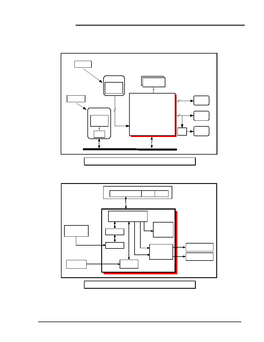
System Diagrams
The 65554 system configurations appear below. Figure 1 shows the connections to external hardware.
NTSC/PAL
Video Input
NTSC/PAL
Video Input
Video Input
Module
Video
Decoder
w/ Scaling
Video
Decoder
w/ Scaling
PCI Bus
Master
Video Input
Module
16-bit
32-bit
32-bit
HiQV64
TM
&+,36
Æ
CRT
Monitor
TV
Monitor
RGB to
NTSC
RGB
24
16-bit
64-bit
System Bus
2 Meg Shared
Frame Buffer
Color
STN/TFT
Figure 1: System Diagram - External Interfaces
Figure 2 shows the data flow within the chip.
Memory
YUVa YUVb
64-bit
RGB
YUV
Memory
Controller
Scaling
Capture
64-bit
Graphics
Engine
YUV to RGB
Color Key Zoom
Bus
Interface
HiQV64
TM
TM
PCI Bus
Digital RGB
RGB
Video
Capture Port
Analog RGB
Figure 2: System Diagram - Internal Data Flow