 | –≠–ª–µ–∫—Ç—Ä–æ–Ω–Ω—ã–π –∫–æ–º–ø–æ–Ω–µ–Ω—Ç: 69000 | –°–∫–∞—á–∞—Ç—å:  PDF PDF  ZIP ZIP |

69000
69000 HiQVideo
TM
Accelerator with
Integrated Memory
Data Sheet
Revision 1.3
August 1998
P
R
E
L
I
M
I
N
A
R
Y

&+,36
Æ
69000 Databook
Subject to Change Without Notice
Preliminary Rev. 1.3 8/31/98
Copyright Notice
Copyright
©
1997-98 Chips and Technologies, Inc., a subsidiary of Intel Corporation. ALL RIGHTS RESERVED.
This manual is copyrighted by Chips and Technologies, Inc., a subsidiary of Intel Corporation. You may not reproduce, transmit,
transcribe, store in a retrieval system, or translate into any language or computer language, in any form or by any means - elec-
tronic, mechanical, magnetic, optical, chemical, manual, or otherwise - any part of this publication without the express written
permission of Chips and Technologies, Inc., a subsidiary of Intel Corporation.
Restricted Rights Legend
Use, duplication, or disclosure by the Government is subject to restrictions set forth in subparagraph (c)(1)(ii) of the Rights in
Technical Data and Computer Software clause at 252.277-7013.
Trademark Acknowledgment
CHIPS Logo is a registered trademark of Chips and Technologies, Inc., a subsidiary of Intel Corporation.
HiQVideo, is a trademark of Chips and Technologies, Inc., a subsidiary of Intel Corporation.
All other trademarks are the property of their respective holders.
Disclaimer
This document provides general information for the customer. Chips and Technologies, Inc., a subsidiary of Intel Corporation,
reserves the right to modify the information contained herein as necessary and the customer should ensure that it has the most
recent revision of the document. CHIPS makes no warranty for the use of its products and bears no responsibility for any errors
which may appear in this document. The customer should be on notice that many different parties hold patents on products,
components, and processes within the personal computer industry. Customers should ensure that their use of the products
does not infringe upon any patents. CHIPS respects the patent rights of third parties and shall not participate in direct or indirect
patent infringement.

&+,36
Æ
69000 Databook
Subject to Change Without Notice
Revision 1.3 8/31/98
T
Highly integrated Flat Panel and CRT GUI
Accelerator & Multimedia Engine,
Palette/DAC, Clock Synthesizer, and
integrated frame buffer
T
Integrated High Performance SDRAM
memory
∑ 2MB integrated memory
∑ 83 MHz SDRAM operation
T
HiQColor
TM
Technology implemented with
TMED (Temporal Modulated Energy
Distribution)
∑ Enables 16.7 Million colors on STN panel
without
dither
∑ Brighter and Crisper STN Image
∑ No shimmer or Mach bands on STN
∑ No crawling images on STN
∑ 256 gray shades per primary color
∑ Panel Tuning NOT required
T
Hardware
Windows
Acceleration
∑ Single Cycle 64-bit Graphics Engine
∑ System-to-Screen and
∑ Screen-to-Screen BitBLT
∑ 3-Operand Raster-Ops
∑ 8/16/24 Color Expansion
∑ Transparent BLT
- Optimized for Windows
TM
BitBLT format
∑ Acceleration in ALL color modes
T
Integrated composite NTSC / PAL Support
∑ Flicker Reduction Circuitry
T
Hardware Multimedia Support
∑ Zoom Video port
∑ YUV input from System Bus or Video Port
∑ YUV-RGB Conversion
∑ Capture / Scaling
∑ Video Zoom up to 8x
∑ Vertical interpolation of video data up to
720 pixels wide.
∑ Double Buffered Video
∑ Horizontal Interpolation
∑ Image Mirroring
T
Display centering and stretching features for
optimal fit of VGA graphics and text on
800x600 and 1024x768 panels
T
Simultaneous Hardware Cursor and Pop-up
Window
∑ 64x64 pixels by 4 colors
∑ 128x128 pixels by 2 colors
T
PCI/Frame AGP Bus with Burst Mode
capability and BIOS ROM support
T
Power Sequencing control outputs regulate
application of bias voltage, +5V to the
panel and +12V to the inverter for
backlight operation.
T
3.3V Operation, 5.0V tolerant I/O
T
Game Acceleration
∑ Source Transparent BLT
∑ Destination Transparent BLT
∑ Double buffer support for YUV and 15/
16Bpp Overlay Engine
∑ Instant Full Screen Page Flip
∑ Read back of CRT Scan line counters
T
High-Performance Flat Panel Display
resolutions and color depth at 3.3V
∑ 640x480 x 24bpp
∑ 800x600 x 24bpp
∑ 1024x768 x 16bpp
∑ 1280x1024 x 8bpp
T
CRT
Support
∑ Integrated high performance triple 8-bit,
RAMDAC
T
Flexible Panel Support
∑ Support for a wide variety of monochrome
and color panels
∑ Single-Panel, Single-Drive (SS)
∑ Dual-Panel, Dual Drive (DD) passive STN
∑ Active matrix TFT/MIM LCD
∑ EL panels
∑ Plasma panels
T
36-bit direct interface to color and
monochrome, single drive (SS), and dual
drive (DD), STN & TFT panels
T
Support for 16:9 aspect ratio panels
T
Flexible On-chip Activity Timer facilitates
ordered shut-down of the display system
T
Advanced Power Management feature
minimizes power usage in:
∑ Normal operation
∑ Standby (Sleep) modes
∑ Panel-Off Power-Saving Mode
T
VESA Standards supported
∑ VAFC Port for display of "Live" Video
∑ DPMS for CRT power-down
∑ DDC for CRT Plug-Play & Display Control
T
Fully Compatible with IBM
Æ
VGA
T
Packages supported
∑ 272 PBGA
∑ 256 mBGA
69000 High Performance Flat Panel / CRT
HiQVideo
TM
Accelerator with
Integrated Memory

&+,36
Æ
69000 Databook
Subject to Change Without Notice
Revision 1.3 8/31/98
T
Drivers Features
∑
High Performance Accelerated drivers
∑
Compatible across HiQVideo family
∑
Auto Panning Support
∑
LCD/CRT/Simultaneous Mode Support
∑
Auto Resolution Change
∑
HW Stretching/Scaling
∑
Double Buffering
∑
Internationalization
∑
ChipsCPL (Control Panel Applet)
∑
Direct Draw support
∑
Games SDK support
∑
Dynamic Resolution Switching
∑
VGA Graphics applications in
Windows
TM
∑
VESA DDC extensions
∑
VESA DPMS extensions
∑
Property Sheet to change Refresh/
Display
∑
Seamless Windows Support
∑
Boot time resolution adjustment
∑
DIVE, EnDIVE
∑
DCAF
T
Multimedia Software
∑
Video Port Manager for ZV Port
∑
PCVideo DLL plus Tuner with DK
Board
T
Software Utilities
∑
DebugVGA
∑
Auto testing of all video modes
∑
ChipsVGA
∑
ChipsEXT
T
Software Documentation
∑
BIOS OEM Reference Guide
∑
Display Driver User's Guide
∑
Utilities User's Guide
∑
Release Notes for BIOS, Drivers, and
Utilities
T
Software Support
∑
Dedicated Software Applications
Engineer
∑
BBS Support for Software Updates
T
BIOS Features
∑
VGA Compatible BIOS
∑
PnP Support
∑
VESA VBE 2.0 (incl. DPMS)
∑
DDC 1, DDC 2AB
∑
Text and Graphics Expansion
∑
Auto Centering
∑
44 (40) K BIOS
∑
CRT, LCD, Simultaneous display
modes
∑
Auto Resolution Switch
∑
Multiple Refresh Rates
∑
NTSC/PAL support
∑
Extended Modes
∑
Extended BIOS Functions
∑
1024x768 TFT, DSTN Color Panels
∑
Multiple Panel Support (8 panels built-
in)
∑
Get Panel Type Function
∑
HW Popup Interface
∑
Monitor Detect
∑
Pop Up Support
∑
SMI and Hot Key support
T
System BIOS Hooks
∑
Set Active Display Type
∑
Save/Restore Video State
∑
Setup Memory for Save/Restore
∑
SMI Entry Point
∑
Int 15 Calls after POST, Set Mode
T
BIOS Modify Program (BMP)
∑
Clocks
∑
Mode support
∑
Panel Tables
∑
Int 15 Hooks
∑
Monitor Sensing
T
Driver Support
∑
Windows 95
∑
Windows NT 4.0, NT 3.1
∑
Windows 98
∑
Win 31
69000 Software Support Features

iii
&+,36
Æ
69000 Databook
Subject to Change Without Notice
Revision 1.3 8/31/98
Revision History
Revision
Date
By
Comments
0.1
2/28/97
TE/lc/bjb
First Draft- Official Release
0.2
4/3/97
AS/bjb
Change MCLK from 110MHz to 83MHz
Added HiQColor(features)
Updated Pin Descriptions
Updated Extension Registers
Update Multimedia Registers
Updated Electrical Specifications
Updated Appendix A
1.0
8/18/97
AS/bjb
Remove NDA requirements and API status
1.1
10/10/97
BB/lnc
Reorganized chapters
Added Wide Extension Register chapter
Updated Flat Panel Registers
Updated CRT Controller Registers
Added Subsystem and Subvendor ID support
1.2
3/9/98
BB/lnc
Improved Status Register Descriptions
Improved Palette Register Chapter
Improved Extension Register Descriptions
Improved Flat Panel Register Descriptions
Improved Multimedia Register Descriptions
Improved BitBLT Engine Register Descriptions
Updated Specifications chapter
1.3
7/1/98
BB/bjb
Added bullet-item for Frame-Based AGP Support
Added mBGA package pinout and pin numbering
Added Frame-Based AGP Interface timings
Added mBGA package mechanical specifications
Add differences between PCI-66/Frame-Based AGP

iv
&+,36
Æ
69000 Databook
Subject to Change Without Notice
Revision 1.3 8/31/98

v
&+,36
Æ
69000 Databook
Subject to Change Without Notice
Revision 1.3 8/31/98
List Of Figures
.................................................................................................................................. xv
List of Tables
................................................................................................................................... xvii
Chapter 1
Introduction / Overview
High Performance Integrated Memory ...................................................................................... 1-1
Frame-Based AGP Compatibility .............................................................................................. 1-1
HiQColor
TM
Technology ........................................................................................................... 1-1
Versatile Panel Support ........................................................................................................... 1-1
Acceleration for All Panels and All Modes ................................................................................ 1-1
Television NTSC/PAL Flicker Free Output................................................................................ 1-1
HiQVideo
TM
Multimedia Support............................................................................................... 1-3
Low Power Consumption .......................................................................................................... 1-3
Software Compatibility/Flexibility............................................................................................... 1-3
Display Modes Supported ......................................................................................................... 1-4
Chapter 2
Pin Descriptions
Pin Diagram, Top View, Ball Grid Array ................................................................................... 2-1
Pin Diagram, Bottom View, Ball Grid Array............................................................................... 2-2
Pin Diagram, Top View, Mini Ball Grid Array ............................................................................ 2-3
Pin Diagram, Bottom View, Mini Ball Grid Array ....................................................................... 2-4
PCI/AGP Bus Interface ............................................................................................................ 2-5
Configuration Pins and ROM Interface .................................................................................... 2-8
Flat Panel Display Interface ...................................................................................................... 2-9
CRT Interface ......................................................................................................................... 2-12
Video Interface ....................................................................................................................... 2-13
Miscellaneous ........................................................................................................................ 2-14
Power and Ground ................................................................................................................. 2-15
Reserved and No Connect ..................................................................................................... 2-17
Chapter 3
Electrical Specifications
Absolute Maximum Conditions.................................................................................................. 3-1
Normal Operating Conditions.................................................................................................... 3-1
DAC Characteristics.................................................................................................................. 3-1
DC Characteristics .................................................................................................................... 3-2
DC Drive Characteristics........................................................................................................... 3-2
AC Test Conditions ................................................................................................................... 3-3
AC Timing Characteristics - Reference Clock........................................................................... 3-4
AC Timing Characteristics - Clock Generator ........................................................................... 3-4
AC Timing Characteristics - Reset ............................................................................................ 3-5
AC Timing Characteristics - PCI Bus Frame (CLK = 33MHz) ................................................... 3-6
AC Timing Characteristics - PCI Bus Stop (CLK = 33MHz) ...................................................... 3-7
AC Timing Characteristics - BIOS ROM ................................................................................... 3-8
AC Timing Characteristics - Video Data Port ............................................................................ 3-9
AC Timing Characteristics - Panel Output Timing................................................................... 3-10
AC Timing Characteristics - A.G.P. 1x AC Timing Parameters............................................... 3-11
Chapter 4
Mechanical Specifications
......................................................................................................... 4-1

vi
&+,36
Æ
69000 Databook
Subject to Change Without Notice
Revision 1.3 8/31/98
Chapter 5
I/O and Memory Address Maps
I/O and Memory Address Map ................................................................................................. 5-1
VGA-Compatible Address Map ................................................................................................. 5-1
Address Maps for Going Beyond VGA...................................................................................... 5-2
PCI Configurations Registers ................................................................................................... 5-3
I/O and Sub-Addressed Register Map ..................................................................................... 5-4
Sub-Addressing Indexes and Data Ports .................................................................................. 5-5
Lower Memory Map .................................................................................................................. 5-6
Upper Memory Map .................................................................................................................. 5-7
Chapter 6
Register Summaries
PCI Configuration Registers ..................................................................................................... 6-1
General Control & Status Registers .......................................................................................... 6-1
CRT Controller Registers .......................................................................................................... 6-2
Sequencer Registers................................................................................................................. 6-3
Graphics Controller Registers ................................................................................................... 6-3
Attribute Controller Registers .................................................................................................... 6-3
Palette Registers....................................................................................................................... 6-3
Extension Registers .................................................................................................................. 6-4
Flat Panel Registers.................................................................................................................. 6-6
Multimedia Registers................................................................................................................. 6-7
BitBLT Registers ....................................................................................................................... 6-8
Memory Mapped Wide Extension Registers ............................................................................ 6-8
Chapter 7
PCI Configuration Registers
VENDID Vendor ID Register .................................................................................................... 7-2
DEVID Device ID Register ....................................................................................................... 7-2
DEVCTL Device Control Register ............................................................................................ 7-3
DEVSTAT Device Status Register ........................................................................................... 7-5
REV Revision ID Register ........................................................................................................ 7-7
PRG Register-Level Programming Interface Register ............................................................. 7-7
SUB Sub-Class Code Register ................................................................................................ 7-8
BASE Base Class Code Register ............................................................................................ 7-8
HDR Header Type Register ..................................................................................................... 7-9
MBASE Memory Base Address Register ............................................................................... 7-10
SUBVENDID Subsystem Vendor ID Register ........................................................................ 7-11
SUBDEVDID Subsystem Device ID Register ......................................................................... 7-11
INTLINE Interrupt Line Register.............................................................................................. 7-12
INTPIN Interrupt Pin Register ................................................................................................. 7-12
RBASE ROM Base Address Register..................................................................................... 7-13
SUBVENDSET Subsystem Vendor ID Set Register ............................................................... 7-14
SUBDEVSET Subsystem Device ID Set Register .................................................................. 7-14
Chapter 8
General Control and Status Registers
ST00 Input Status Register 0 ................................................................................................... 8-2
ST01 Input Status Register 1 .................................................................................................. 8-3
FCR Feature Control Register ................................................................................................. 8-4
MSR Miscellaneous Output Register ....................................................................................... 8-5

vii
&+,36
Æ
69000 Databook
Subject to Change Without Notice
Revision 1.3 8/31/98
Chapter 9
CRT Controller Registers
CRX CRT Controller Index Register .................................................................................. 9-2
CR00 Horizontal Total Register ........................................................................................... 9-3
CR01 Horizontal Display Enable End Register .................................................................... 9-3
CR02 Horizontal Blanking Start Register ............................................................................. 9-3
CR03 Horizontal Blanking End Register .............................................................................. 9-4
CR04 Horizontal Sync Start Register ................................................................................... 9-5
CR05 Horizontal Sync End Register .................................................................................... 9-6
CR06 Vertical Total Register ................................................................................................ 9-7
CR07 Overflow Register ...................................................................................................... 9-8
CR08 Preset Row Scan Register ....................................................................................... 9-12
CR09 Maximum Scanline Register .................................................................................... 9-13
CR0A Text Cursor Start Register ....................................................................................... 9-15
CR0B Text Cursor End Register ........................................................................................ 9-16
CR0C Start Address High Register .................................................................................... 9-17
CR0D Start Address Low Register ..................................................................................... 9-18
CR0E Text Cursor Location High Register ........................................................................ 9-19
CR0F Text Cursor Location Low Register ......................................................................... 9-19
CR10 Vertical Sync Start Register ..................................................................................... 9-20
CR11 Vertical Sync End Register ...................................................................................... 9-21
CR12 Vertical Display Enable End Register ...................................................................... 9-22
CR13 Offset Register ......................................................................................................... 9-22
CR14 Underline Location Register ..................................................................................... 9-23
CR15 Vertical Blanking Start Register ............................................................................... 9-24
CR16 Vertical Blanking End Register ................................................................................ 9-24
CR17 CRT Mode Control ................................................................................................... 9-25
CR18 Line Compare Register ............................................................................................ 9-28
CR22 Memory Read Latch Data Register .......................................................................... 9-28
CR30 Extended Vertical Total Register ............................................................................. 9-29
CR31 Extended Vertical Display End Register .................................................................. 9-29
CR32 Extended Vertical Sync Start Register ..................................................................... 9-30
CR33 Extended Vertical Blanking Start Register ............................................................... 9-31
CR38 Extended Horizontal Total Register ......................................................................... 9-32
CR3C Extended Horizontal Blanking End Register ............................................................. 9-33
CR40 Extended Start Address Register.............................................................................. 9-34
CR41 Extended Offset Register ......................................................................................... 9-35
CR70 Interlace Control Register ........................................................................................ 9-35
CR71 NTSC/PAL Video Output Control Register .............................................................. 9-36
CR72 NTSC/PAL Horizontal Serration 1 Start Register ..................................................... 9-37
CR73 NTSC/PAL Horizontal Serration 2 Start Register ..................................................... 9-37
CR74 NTSC/PAL Horizontal Pulse Width Register ............................................................ 9-38
CR75 NTSC/PAL Filtering Burst Read Length Register .................................................... 9-39
CR76 NTSC/PAL Filtering Burst Read Quantity Register .................................................. 9-39
CR77 NTSC/PAL Filtering Control Register ....................................................................... 9-40
CR78 NTSC/PAL Vertical Reduction Register.................................................................... 9-41
CR79 NTSC/PAL Horizontal Total Fine Adjust Register..................................................... 9-42

viii
&+,36
Æ
69000 Databook
Subject to Change Without Notice
Revision 1.3 8/31/98
Chapter 10
Sequencer Registers
SRX Sequencer Index Register ....................................................................................... 10-2
SR00 Reset Register ......................................................................................................... 10-2
SR01 Clocking Mode Register ........................................................................................... 10-3
SR02 Plane Mask Register ................................................................................................ 10-4
SR03 Character Map Select Register ................................................................................ 10-5
SR04 Memory Mode Register ............................................................................................ 10-6
SR07 Horizontal Character Counter Reset Register .......................................................... 10-7
Chapter 11
Graphics Controller Registers
GRX Graphics Controller Index Register ......................................................................... 11-2
GR00 Set/Reset Register ................................................................................................... 11-2
GR01 Enable Set/Reset Register ...................................................................................... 11-3
GR02 Color Compare Register .......................................................................................... 11-3
GR03 Data Rotate Register ............................................................................................... 11-4
GR04 Read Plane Select Register ..................................................................................... 11-5
GR05 Graphics Mode Register .......................................................................................... 11-6
GR06 Miscellaneous Register ............................................................................................ 11-9
GR07 Color Don't Care Register ...................................................................................... 11-10
GR08 Bit Mask Register ................................................................................................... 11-10
Chapter 12
Attribute Controller Registers
ARX Attribute Controller Index Register ........................................................................... 12-2
AR00-AR0F Palette Registers 0-F ..................................................................................... 12-2
AR10 Mode Control Register ............................................................................................. 12-3
AR11 Overscan Color Register .......................................................................................... 12-4
AR12 Memory Plane Enable Register ............................................................................... 12-5
AR13 Horizontal Pixel Panning Register ............................................................................ 12-6
AR14 Color Select Register ............................................................................................... 12-7
Chapter 13
Palette Registers
PALMASK Palette Data Mask Register .............................................................................. 13-3
PALSTATE Palette State Register ....................................................................................... 13-3
PALRX Palette Read Index Register ............................................................................ 13-4
PALWX Palette Write Index Register ............................................................................. 13-4
PALDATA Palette Data Register ........................................................................................ 13-5
Chapter 14
Extension Registers
XRX Extension Register Index Register .......................................................................... 14-3
XR00 Vendor ID Low Register ........................................................................................... 14-3
XR01 Vendor ID High Register .......................................................................................... 14-4
XR02 Device ID Low Register ............................................................................................ 14-4
XR03 Device ID High Register ........................................................................................... 14-5
XR04 Revision ID Register ................................................................................................ 14-5
XR05 Linear Base Address Low Register .......................................................................... 14-6
XR06 Linear Base Address High Register ......................................................................... 14-6
XR08 Host Bus Configuration Register .............................................................................. 14-7
XR09 I/O Control Register .................................................................................................. 14-8

ix
&+,36
Æ
69000 Databook
Subject to Change Without Notice
Revision 1.3 8/31/98
XR0A Frame Buffer Mapping Register ............................................................................... 14-9
XR0B PCI Burst Write Support Register .......................................................................... 14-12
XR0E Frame Buffer Page Select Register ....................................................................... 14-12
XR20 BitBLT Configuration Register ................................................................................ 14-13
XR40 Memory Access Control Register ........................................................................... 14-14
XR41-XR4F Memory Configuration Registers ................................................................. 14-14
XR60 Video Pin Control Register ..................................................................................... 14-15
XR61 DPMS Sync Control Register ................................................................................. 14-16
XR62 GPIO Pin Control Register ..................................................................................... 14-17
XR63 GPIO Pin Data Register ......................................................................................... 14-18
XR67 Pin Tri-State Control Register ................................................................................ 14-19
XR70 Configuration Pins 0 Register ................................................................................ 14-20
XR71 Configuration Pins 1 Register ................................................................................ 14-22
XR80 Pixel Pipeline Configuration 0 Register .................................................................. 14-23
XR81 Pixel Pipeline Configuration 1 Register .................................................................. 14-25
XR82 Pixel Pipeline Configuration 2 Register .................................................................. 14-26
XRA0 Cursor 1 Control Register ...................................................................................... 14-27
XRA1 Cursor 1 Vertical Extension Register ..................................................................... 14-28
XRA2 Cursor 1 Base Address Low Register .................................................................... 14-28
XRA3 Cursor 1 Base Address High Register ................................................................... 14-29
XRA4 Cursor 1 X-Position Low Register .......................................................................... 14-29
XRA5 Cursor 1 X-Position High Register ......................................................................... 14-30
XRA6 Cursor 1 Y-Position Low Register .......................................................................... 14-30
XRA7 Cursor 1 Y-Position High Register ......................................................................... 14-31
XRA8 Cursor 2 Control Register ...................................................................................... 14-32
XRA9 Cursor 2 Vertical Extension Register ..................................................................... 14-33
XRAA Cursor 2 Base Address Low Register ................................................................... 14-33
XRAB Cursor 2 Base Address High Register .................................................................. 14-34
XRAC Cursor 2 X-Position Low Register ......................................................................... 14-34
XRAD Cursor 2 X-Position High Register ........................................................................ 14-35
XRAE Cursor 2 Y-Position Low Register ......................................................................... 14-35
XRAF Cursor 2 Y-Position High Register ......................................................................... 14-36
XRC0 Dot Clock 0 VCO M-Divisor Register ..................................................................... 14-36
XRC1 Dot Clock 0 VCO N-Divisor Register ..................................................................... 14-37
XRC3 Dot Clock 0 Divisor Select Register ....................................................................... 14-38
XRC4 Dot Clock 1 VCO M-Divisor Register ..................................................................... 14-39
XRC5 Dot Clock 1 VCO N-Divisor Register ..................................................................... 14-39
XRC7 Dot Clock 1 Divisor Select Register ....................................................................... 14-40
XRC8 Dot Clock 2 VCO M-Divisor Register ..................................................................... 14-41
XRC9 Dot Clock 2 VCO N-Divisor Register ..................................................................... 14-41
XRCB Dot Clock 2 Divisor Select Register ...................................................................... 14-42
XRCC Memory Clock VCO M-Divisor Register ................................................................ 14-43
XRCD Memory Clock VCO N-Divisor Register ................................................................. 14-43
XRCE Memory Clock Divisor Select Register .................................................................. 14-44
XRCF Clock Configuration Register ................................................................................. 14-45
XRD0 Powerdown Control Register ................................................................................. 14-46
XRD1 Power Conservation Control Register ................................................................... 14-47
XRD2 2KHz Down Counter Register ............................................................................... 14-47
XRE0-XREB Software Flag Registers 0 to B ................................................................... 14-48
XRF8-XRFC Test Registers ............................................................................................. 14-48
Chapter 15
Flat Panel Registers
FR00 Feature Register ....................................................................................................... 15-2
FR01 CRT / FP Control Register ....................................................................................... 15-2

x
&+,36
Æ
69000 Databook
Subject to Change Without Notice
Revision 1.3 8/31/98
FR03 FP Dot Clock Source Register ................................................................................. 15-3
FR04 Panel Power Sequencing Delay Register ................................................................ 15-4
FR05 Power Down Control 1 Register ............................................................................... 15-5
FR06 FP Power Down Control Register ............................................................................ 15-6
FR08 FP Pin Polarity Register ........................................................................................... 15-7
FR0A Programmable Output Drive Register ...................................................................... 15-8
FR0B FP Pin Control 1 Register ......................................................................................... 15-9
FR0C Pin Control 2 Register ............................................................................................ 15-10
FR0F Activity Timer Control Register ............................................................................... 15-11
FR10 FP Format 0 Register ............................................................................................. 15-12
FR11 FP Format 1 Register ............................................................................................. 15-14
FR12 FP Format 2 Register ............................................................................................ 15-16
FR13 FP Format 3 Register ............................................................................................ 15-18
FR16 FRC Option Select Register .................................................................................. 15-19
FR17 Polynomial FRC Control Register .......................................................................... 15-20
FR18 FP Text Mode Control Register .............................................................................. 15-20
FR19 Blink Rate Control Register .................................................................................... 15-21
FR1A STN-DD Buffering Control Register ....................................................................... 15-22
FR1E M (ACDCLK) Control Register ............................................................................... 15-22
FR1F Diagnostic Register ................................................................................................ 15-23
FR20 FP Horizontal Panel Display Size LSB Register .................................................... 15-24
FR21 FP Horizontal Sync Start LSB Register .................................................................. 15-24
FR22 FP Horizontal Sync End Register ........................................................................... 15-25
FR23 FP Horizontal Total LSB Register .......................................................................... 15-25
FR24 FP HSync (LP) Delay LSB Register ....................................................................... 15-26
FR25 FP Horizontal Overflow 1 Register ......................................................................... 15-26
FR26 FP Horizontal Overflow 2 Register ......................................................................... 15-27
FR27 FP HSync (LP) Width and Disable Register ........................................................... 15-27
FR30 FP Vertical Panel Size LSB Register ..................................................................... 15-28
FR31 FP Vertical Sync Start LSB (FR31) Register .......................................................... 15-28
FR32 FP Vertical Sync End Register ............................................................................... 15-29
FR33 FP Vertical Total Register ...................................................................................... 15-29
FR34 FP VSync (FLM) Delay Register ............................................................................ 15-30
FR35 FP Vertical Overflow 1 Register ............................................................................. 15-30
FR36 FP Vertical Overflow 2 Register ............................................................................. 15-31
FR37 FP VSync (FLM) Disable ........................................................................................ 15-31
FR40 Horizontal Compensation Register ......................................................................... 15-32
FR41 Horizontal Stretching Register ................................................................................ 15-34
FR48 Vertical Compensation Register ............................................................................. 15-35
FR49-4C Text Mode Vertical Stretching Register ............................................................ 15-36
FR4D Vertical Line Replication Register .......................................................................... 15-36
FR4E Selective Vertical Stretching Disable Register ....................................................... 15-37
FR70 TMED Red Seed Register ...................................................................................... 15-38
FR71 TMED Green Seed Register .................................................................................. 15-38
FR72 TMED Blue Seed Register ..................................................................................... 15-38
FR73 TMED Control Register .......................................................................................... 15-39
FR74 TMED2 Control Register ......................................................................................... 15-40
Chapter 16
Multimedia Registers
MR00 Module Capability Register ...................................................................................... 16-2
MR01 Secondary Capability Register ................................................................................ 16-2
MR02 Capture Control 1 Register ...................................................................................... 16-3
MR03 Capture Control 2 Register ...................................................................................... 16-4
MR04 Capture Control 3 Register ...................................................................................... 16-5

xi
&+,36
Æ
69000 Databook
Subject to Change Without Notice
Revision 1.3 8/31/98
MR05 Capture Control 4 Register ...................................................................................... 16-6
MR06 Capture Memory Address PTR1 Low Register ....................................................... 16-7
MR07 Capture Memory Address PTR1 Mid Register ........................................................ 16-7
MR08 Capture Memory Address PTR1 High Register ....................................................... 16-7
MR09 Capture Memory Address PTR2 Low Register ....................................................... 16-8
MR0A Capture Memory Address PTR2 Mid Register ........................................................ 16-8
MR0B Capture Memory Address PTR2 High Register ...................................................... 16-8
MR0C Capture Line Memory Storage Width Register ....................................................... 16-9
MR0E Capture Window X-LEFT Low Register .................................................................. 16-9
MR0F Capture Window X-LEFT High Register .................................................................. 16-9
MR10 Capture Window X-RIGHT Low Register .............................................................. 16-10
MR11 Capture Window X-RIGHT High Register ............................................................. 16-10
MR12 Capture Window Y-TOP Low Register .................................................................. 16-11
MR13 Capture Window Y-TOP High Register ................................................................. 16-11
MR14 Capture Window Y-BOTTOM Low Register .......................................................... 16-12
MR15 Capture Window Y-BOTTOM High Register ......................................................... 16-12
MR16 H-SCALE Register ................................................................................................. 16-13
MR17 V-SCALE Register ................................................................................................. 16-13
MR18 Capture Frame/Field Count Register .................................................................... 16-13
MR1E Playback Control 1 Register .................................................................................. 16-14
MR1F Playback Control 2 Register .................................................................................. 16-15
MR20 Playback Control 3 Register .................................................................................. 16-16
MR21 Double Buffer Status Register ............................................................................... 16-17
MR22 Playback Memory Address PTR1 Low Register .................................................... 16-18
MR23 Playback Memory Address PTR1 Mid Register .................................................... 16-18
MR24 Playback Memory Address PTR1 High Register ................................................... 16-18
MR25 Playback Memory Address PTR2 Low Register .................................................... 16-19
MR26 Playback Memory Address PTR2 Mid Register .................................................... 16-19
MR27 Playback Memory Address PTR2 High Register ................................................... 16-19
MR28 Playback Line Memory Fetch Width Register ........................................................ 16-20
MR2A Playback Window X-LEFT Low Register .............................................................. 16-20
MR2B Playback Window X-LEFT High Register .............................................................. 16-20
MR2C Playback Window X-RIGHT Low Register ............................................................ 16-21
MR2D Playback Window X-RIGHT High Register ........................................................... 16-21
MR2E Playback Window Y-TOP Low Register ................................................................ 16-22
MR2F Playback Window Y-TOP High Register ............................................................... 16-22
MR30 Playback Window Y-BOTTOM Low Register ........................................................ 16-23
MR31 Playback Window Y-BOTTOM High Register ....................................................... 16-23
MR32 H-ZOOM Register .................................................................................................. 16-24
MR33 V-ZOOM Register .................................................................................................. 16-24
MR34 Playback Line Display Width Register ................................................................... 16-25
MR3C Color Key Control 1 Register ................................................................................ 16-25
MR3D-3F Color Key Registers ......................................................................................... 16-26
MR40-42 Color Key Mask Registers ................................................................................ 16-26
MR43 Line Count Low Register ....................................................................................... 16-27
MR44 Line Count High Register ...................................................................................... 16-27
Chapter 17
BitBLT Registers
BR00 Source and Destination Span Register .................................................................... 17-2
BR01 Pattern/Source Expansion Background Color & Transparency Key Register .......... 17-3
BR02 Pattern/Source Expansion Foreground Color Register ............................................ 17-4
BR03 Monochrome Source Control Register ..................................................................... 17-5
BR04 BitBLT Control Register ........................................................................................... 17-7
BR05 Pattern Address Register ....................................................................................... 17-11
BR06 Source Address Register ....................................................................................... 17-12

xii
&+,36
Æ
69000 Databook
Subject to Change Without Notice
Revision 1.3 8/31/98
BR07 Destination Address Register ................................................................................. 17-13
BR08 Destination Width & Height Register ...................................................................... 17-14
BR09 Source Expansion Background Color & Transparency Key Register .................... 17-15
BR0A Source Expansion Foreground Color Register ...................................................... 17-16
Chapter 18
Memory-Mapped Wide Extension Registers
ER00 Central Interrupt Control Register ............................................................................ 18-2
ER01 Central Interrupt Status/Acknowledge Register ....................................................... 18-3
ER03 Miscellaneous Function Register ............................................................................. 18-4
Appendix A
Display Modes
.................................................................................................................................A-1
CRT-Only Display Modes .........................................................................................................A-2
Standard VGA CRT-Only Display Modes .................................................................................A-2
Chips Extended VGA CRT-Only Display Modes.......................................................................A-3
Display Modes...........................................................................................................................A-6
Flat Panel-Only and Simultaneous 640x480 (VGA) Display Modes .........................................A-6
Flat Panel-Only and Simultaneous 800x600 (SVGA) Display Modes.......................................A-7
Flat Panel-Only and Simultaneous 1024x768 Display Modes ..................................................A-8
Flat Panel-Only and Simultaneous 1280x1024 Display Modes ................................................A-9
Appendix B
Clock Generation
...........................................................................................................................B-1
Clock Synthesizer ....................................................................................................................B-1
Dot Clock (DCLK) .....................................................................................................................B-1
Memory Clock (MCLK) .............................................................................................................B-1
PLL Parameters .......................................................................................................................B-2
Programming the Clock Synthesizer.........................................................................................B-3
DCLK Programming ..................................................................................................................B-3
MCLK Programming..................................................................................................................B-3
Programming Constraints .........................................................................................................B-4
Programming Example .............................................................................................................B-4
PCB Layout Considerations .....................................................................................................B-5
Display Memory Bandwidth ......................................................................................................B-7
STN-DD Panel Buffering ..........................................................................................................B-8
Horizontal and Vertical Clocking ..............................................................................................B-9
Appendix C
Panel Power Sequencing
........................................................................................................... C-1
Appendix D
Hardware Cursor and Pop Up Window
................................................................................ D-1
Basic Cursor Configuration ..................................................................................................... D-1
Base Address for Cursor Data ................................................................................................ D-2
Cursor Vertical Extension ........................................................................................................ D-2
Cursor Colors .......................................................................................................................... D-2
Cursor Positioning ................................................................................................................... D-3
Cursor Modes .......................................................................................................................... D-3
32x32x2bpp & 64x64x2bpp AND/XOR Pixel Plane Modes .................................................... D-4
64x64x2bpp 4-Color Mode ...................................................................................................... D-6
64x64x2bpp 3-Color and Transparency Mode ........................................................................ D-7
128x128x1bpp 2-Color Mode .................................................................................................. D-8
128x128x1bpp 1-Color and Transparency Mode .................................................................... D-9

xiii
&+,36
Æ
69000 Databook
Subject to Change Without Notice
Revision 1.3 8/31/98
Appendix E
BitBLT Operation
.......................................................................................................................... E-1
Introduction ............................................................................................................................. E-1
Color Depth Configuration and Color Expansion .................................................................... E-2
Graphics Data Size Limitations ............................................................................................... E-3
Bit-Wise Operations ................................................................................................................ E-3
Per-Pixel Write-Masking Operations ....................................................................................... E-7
When the Source and Destination Locations Overlap ............................................................ E-8
Contiguous vs. Discontiguous Graphics Data ....................................................................... E-12
Source Data .......................................................................................................................... E-13
Monochrome Source Data .................................................................................................... E-14
Pattern Data .......................................................................................................................... E-14
Destination Data .................................................................................................................... E-17
BitBLT Programming Examples Pattern Fill -- A Very Simple BitBLT ................................... E-18
Drawing Characters Using a Font Stored in System Memory ............................................... E-20

xiv
&+,36
Æ
69000 Databook
Subject to Change Without Notice
Revision 1.3 8/31/98

xv
&+,36
Æ
69000 Databook
Subject to Change Without Notice
Revision 1.3 8/31/98
List Of Figures
Figure 1-1: Pixel Averaging Circuit .......................................................................................... 1-2
Figure 1-3: Data Pipeline After MMUX, 2 Clocking .................................................................. 1-4
Figure 2-1: Pin Diagram, Top View, Ball Grid Array................................................................. 2-1
Figure 2-2: Pin Diagram, Bottom View, Ball Grid Array ........................................................... 2-2
Figure 2-3: Pin Diagram, Top View, Mini Ball Grid Array ......................................................... 2-3
Figure 2-4: Pin Diagram, Bottom View, Mini Ball Grid Array .................................................... 2-4
Figure 3-1: AC Test Timing ..................................................................................................... 3-3
Figure 3-2: Reference Clock Timing ....................................................................................... 3-4
Figure 3-3: Reset Timing ......................................................................................................... 3-5
Figure 3-4: PCI Bus Frame Timing ......................................................................................... 3-6
Figure 3-5: PCI Bus Stop Timing ............................................................................................ 3-7
Figure 3-6: BIOS ROM Timing ................................................................................................ 3-8
Figure 3-7: Video Data Port Timing ......................................................................................... 3-9
Figure 3-8: Panel Output Timing ........................................................................................... 3-10
Figure 4-1: 256+16 - Contact Ball Grid Array ......................................................................... 4-1
Figure 4-2: 256 Ball - mini Ball Grid Array................................................................................ 4-2
Figure B-1: PLL Elements ....................................................................................................... B-2
Figure E-1: Block Diagram and Data Paths of the BitBLT Engine ......................................... E-1
Figure E-2: Block Diagram and Data Paths of the BitBLT Engine ......................................... E-7
Figure E-3: Source Corruption in BitBLT with Overlapping Source and Destination ............ E-8
Figure E-4: Correctly Performed BitBLT with Overlapping Source and Destination ........... E-10
Figure E-5: Suggested Starting Points for Source and Destination Overlap Situations ....... E-11
Figure E-6: On-Screen Single 6-Pixel Line in the Frame Buffer .......................................... E-12
Figure E-7: On-Screen 6x4 Array of Pixels in the Frame Buffer .......................................... E-13
Figure E- 8: Pattern Data ..................................................................................................... E-15
Figure E-9: Monochrome Pattern Data -- Occupies a Single Quadword ............................. E-15
Figure E-10: 8bpp Pattern Data -- Occupies 64 Bytes (8 Quadwords) ................................ E-15
Figure E-11: 16bpp Pattern Data -- Occupies 128 Bytes (16 Quadwords) .......................... E-16
Figure E-12: 24bpp Pattern Data -- Occupies 256 Bytes (32 Quadwords) .......................... E-16
Figure E-13: On-Screen Destination for Example Pattern Fill BitBLT .................................. E-18
Figure E-14: Pattern Data for Example Pattern Fill BitBLT .................................................. E-19
Figure E-15: Results of Example Pattern Fill BitBLT ........................................................... E-20
Figure E-16: On-Screen Destination for Example Character Drawing BitBLT ..................... E-21
Figure E- 17: Source Data in System Memory for Example Character Drawing BitBLT ...... E-21
Figure E-18: Results of Example Character Drawing BitBLT ............................................... E-23

xvi
&+,36
Æ
69000 Databook
Subject to Change Without Notice
Revision 1.3 8/31/98

xvii
&+,36
Æ
69000 Databook
Subject to Change Without Notice
Revision 1.3 8/31/98
List of Tables
Table 1-1: 69000 Mode Support .............................................................................................. 1-4
Table 3-1: Absolute Maximum Conditions .............................................................................. 3-1
Table 3-2: Normal Operating Conditions ................................................................................. 3-1
Table 3-3: DAC Characteristics ...............................................................................................3-1
Table 3-4: DC Characteristics ................................................................................................. 3-2
Table 3-5: DC Drive Characteristics ........................................................................................ 3-2
Table 3-6: AC Test Conditions ................................................................................................ 3-3
Table 3-7: AC Timing Characteristics - Reference Clock ........................................................ 3-4
Table 3-8: AC Timing Characteristics - Clock Generator ........................................................ 3-4
Table 3-9: AC Timing Characteristics - Reset ......................................................................... 3-5
Table 3-10: AC Timing Characteristics - PCI Bus Frame (CLK = 33MHz) ............................... 3-6
Table 3-11: AC Timing Characteristics - PCI Bus Stop (CLK = 33MHz) .................................. 3-7
Table 3-12: AC Timing Characteristics - BIOS ROM ............................................................... 3-8
Table 3-13: AC Timing Characteristics - Video Data Port ........................................................ 3-9
Table 3-14: AC Timing Characteristics - Panel Output Timing .............................................. 3-10
Table 3-15: AC Timing Characteristics - A.G.P. 1x AC Timing Parameters ........................... 3-11
Table 6-1: PCI Configuration Registers ................................................................................. 6-1
Table 6-2: General Control & Status Registers ....................................................................... 6-1
Table 6-3: CRT Controller Registers ....................................................................................... 6-2
Table 6-4: Sequencer Registers ............................................................................................. 6-3
Table 6-5: Graphics Controller Registers ................................................................................ 6-3
Table 6-6: Attribute Controller Registers ................................................................................. 6-3
Table 6-7: Palette Registers ..................................................................................................... 6-3
Table 6-8: Extension Registers ............................................................................................... 6-4
Table 6-9: Flat Panel Registers ............................................................................................... 6-6
Table 6-10: Multimedia Registers ............................................................................................ 6-7
Table 6-11: BitBLT Registers .................................................................................................. 6-8
Table 6-12: Memory Mapped Wide Extension Registers ........................................................ 6-8
Table 7-1: PCI Configuration Registers .................................................................................. 7-1
Table 15-1: Flat Panel Registers ........................................................................................... 15-1
Table 16-1: Multimedia Registers ......................................................................................... 16-1
Table 16-2: Color Key Bit Assignments ............................................................................... 16-26
Table A-1: Standard VGA CRT-Only Display Modes ............................................................. A-2
Table A-2: Extended VGA CRT-Only Display Modes ............................................................. A-3
Table A-3: Flat Panel-Only and Simultaneous 640x480 (VGA) Display Modes...................... A-6
Table A-4: Flat Panel-Only and Simultaneous Display Modes for 800x600 Panels ............... A-7
Table A-5: Flat Panel-Only and Simultaneous Display Modes for 1024x768 Flat Panels ...... A-8
Table A-6: Flat Panel-Only and Simultaneous Display Modes for 1280x1024 Flat Panel ...... A-9
Table D-1: Memory Organization 32x32x2bpp AND/XOR Pixel Plane Mode ........................ D-4
Table D-2: Memory Organization 64x64x2bpp AND/XOR Pixel Plane Mode ......................... D-5
Table D-3: Pixel Data 32x32x2bpp and 64x64x2bpp AND/XOR Pixel Plane Modes ............. D-5
Table D-4: Memory Organization 64x64x2bpp 4-Color Mode ................................................ D-6
Table D- 5: Pixel Data 64x64x2bpp 4-Color Mode .................................................................. D-6
Table D-6: Memory Organization 64x64x2bpp 3-Color & Transparency Mode ..................... D-7
Table D-7: Pixel Data 64x64x2bpp 3-Color & Transparency Mode ...................................... D-7
Table D-8: Memory Organization 128x128x1bpp 2-Color Mode ............................................ D-8
Table D-9: Pixel Data 128x128x1bpp 2-Color Mode .............................................................. D-8
Table D-10: Memory Organization 128x128x1bpp 1-Color & Transparency Mode ............... D-9
Table D-11: Pixel Bit Definitions 128x128x1bpp 1-Color & Transparency Mode ................... D-9
Table E-1: Bit-Wise Operations and 8-bit Codes (00 - 5F) .................................................... E-4
Table E-2: Bit-Wise Operations and 8-bit Codes (60 - BF) .................................................... E-5
Table E-3: Bit-Wise Operations and 8-bit Codes (C0 - FF) .................................................... E-6

xviii
&+,36
Æ
69000 Databook
Subject to Change Without Notice
Revision 1.3 8/31/98

Introduction / Overview
1-1
&+,36
Æ
69000 Databook
Subject to Change Without Notice
Revision 1.3 8/31/98
Chapter 1
Introduction / Overview
The 69000 is the first product in the CHIPS family of portable graphics accelerator product line that
integrates high performance memory technology for the graphics frame buffer. Based on the proven
HiQVideo
TM
graphics accelerator core, the 69000 combines state-of-the-art flat panel controller capabilities
with low power, high performance integrated memory. The result is the start of a high performance, low
power, highly integrated solution for the premier family of portable graphics products.
High Performance Integrated Memory
The 69000 is the first member of the HiQVideo
TM
family to provide integrated high performance
synchronous DRAM (SDRAM) memory technology. Targeted at the mainstream notebook market, the
69000 incorporates 2MB of proprietary integrated SDRAM for the graphics/video frame buffer. The
integrated SDRAM memory can support up to 83MHz operation, thus increasing the available memory
bandwidth for the graphics subsystem. The result is support for additional high color / high resolution
graphics modes combined with real-time video acceleration. This additional bandwidth also allows more
flexibility in the other graphics functions intensely used in Graphical User Interfaces (GUIs) such as
Microsoft
TM
Windows
TM.
Frame-Based AGP Compatibility
The 69000 graphics is designed to be used with either 33MHz PCI, or with AGP as a frame-based AGP
device, allowing it to be used with the AGP interface provided by the latest core logic chipsets.
HiQColor
TM
Technology
The 69000 integrates CHIPS breakthrough HiQColor
TM
technology. Based on the CHIPS proprietary
TMED
TM
(Temporal Modulated Energy Distribution) algorithm, HiQColor technology is a unique process that
allows the display of 16.7 million true colors on STN panels without using Frame Rate Control (FRC) or
dithering. In addition, TMED also reduces the need for the panel tuning associated with current FRC-based
algorithms. Independent of panel response, the TMED algorithm eliminates all of the flaws (such as
shimmer, Mach banding, and other motion artifacts) normally associated with dithering and FRC. Combined
with the new fast response, high-contrast, and low-crosstalk technology found in new STN panels, HiQColor
technology enables the best display quality and color fidelity previously only available with TFT technology.
Versatile Panel Support
The HiQVideo
TM
family supports a wide variety of monochrome and color Single-Panel, Single-Drive (SS)
and Dual-Panel, Dual Drive (DD), standard and high-resolution, passive STN and active matrix TFT/MIM
LCD, and EL panels. With HiQColor
TM
technology, up to 256 gray scales are supported on passive STN
LCDs. Up to 16.7M different colors can be displayed on passive STN LCDs and up to 16.7M colors on 24-
bit active matrix LCDs.
The 69000 offers a variety of programmable features to optimize display quality. Vertical centering and
stretching are provided for handling modes with less than 480 lines on 480-line panels. Horizontal and
vertical stretching capabilities are also available for both text and graphics modes for optimal display of VGA
text and graphics modes on 800x600, 1024x768 and 1280x1024 panels.
Television NTSC/PAL Flicker Free Output
The 69000 uses a flicker reduction process which makes text of all fonts and sizes readable by reducing the
flicker and jumping lines on the display. To accomplish this, the 69000 uses a line buffer and digital filters
to average adjacent vertical lines for odd/even display. The chip also uses both horizontal and vertical
interpolation to make both graphics and text appear "smooth" on the television. This process reduces the
effect of flicker in the NTSC mode.

1-2
Introduction / Overview
&+,36
Æ
69000 Databook
Subject to Change Without Notice
Revision 1.3 8/31/98
Flicker reduction can be accomplished by averaging the contents of successive horizontal and vertical lines.
See Figure 1-1. The flicker reduction circuit is in pixel data path, with the vertical averaging circuit followed
by the horizontal averaging circuit. Both have bypass controls (Vertical filter enable and Horizontal filter
enable). This flicker averaging circuit is placed before the DAC and before the flat panel pick off. The flat
panel pins can be used for test verification of correct filter operation.
Figure 1-1: Pixel Averaging Circuit
For the non-flicker reduction mode, the display line data is stored sequentially in the FIFO buffer. For the
flicker reduction mode the FIFO buffer data is written in strips of
segments
because the vertical filter
averages the current and next line pixels. Each segment is written to alternate locations in the FIFO buffer.
See Fig. 1-2.
The write pointer is modified to skip through the FIFO buffer. A current/next line flag is carried through the
display pipeline to keep track of which line the pixel comes from. This is needed for the color key logic and
the vertical filter averaging circuitry to align to the correct segment of pixels. The MMUX color key is formed
on the "current" pixel pair.
Flicker reduced NTSC is supported in the following extended graphics modes:
NTSC:
640x480, 60 Hz Interlaced
PAL:
800x600, 50 Hz, Interlaced
Color Depths:
8 bit indexed
15 bit RGB
16 bit RGB
24 bit RGB
NO RM A L
VE RT ICA L A V E RA G ING
VE RT ICA L A N D H O R IZ O NT A L
AV ER AG IN G
FIG . 1
HO RIZ O N T AL A V E R A G IN G
F U L L B L AC K
3 /4 B LA C K
1 /2 B LA C K
1 /4 B LA C K
1 /8 B LA C K
W H ITE

Introduction / Overview
1-3
&+,36
Æ
69000 Databook
Subject to Change Without Notice
Revision 1.3 8/31/98
The television output circuitry supports both NTSC and PAL standard formats, and scales images
appropriately for both television formats and
panels.
HiQVideo
TM
Multimedia Support
The 69000 uses independent multimedia capture and display systems on-chip. The capture system places
data in display memory (usually off screen) and the display system places the data in a window on the
screen.
The capture system can receive data from either the system bus or from the ZV enabled video port in either
RGB or YUV format. The input data can also be scaled down before storage in display memory. Capture
of input data may also be double buffered for smoothing and to prevent image tearing. To better support
MPEG2 (DVD) video decompression, the 69000 includes a line buffer to directly support the native format
of MPEG2 data of 720 pixels wide.
The capture engine also supports image mirroring and rotation for camera support. This feature is important
for applications such as video teleconferencing because it allows the image movements to appear on the
display as it actually occurs. The image and movement is not a mirror image of what is actually taking place.
The display system can independently place either RGB or YUV data from anywhere in display memory into
an on-screen window which can be any size and located at any pixel boundary (YUV data is converted to
RGB "on-the-fly" on output). This is important for the 69000 since the video must be stored in the integrated
2MB frame buffer and thus optimized to require very little space. Storing data in the native YUV format uses
less memory for video while providing excellent playback display quality.
Non-rectangular windows are supported via color keying. The data can be fractionally zoomed on output
up to 8x to fit the on-screen window and can be horizontally and vertically interpolated. Interlaced and non-
interlaced data are both supported in the capture and display systems.
Low Power Consumption
The 69000 uses a variety of advanced power management features to reduce power consumption of the
display sub-system and to extend battery life. Optimized for 3.3V operation, the 69000 internal logic, bus
and panel interfaces operate at 3.3V but can tolerate 5V operation.
Software Compatibility / Flexibility
The HiQVideo controllers are fully compatible with the VGA standard at both the register and BIOS levels.
CHIPS and third-party vendors supply a fully VGA compatible BIOS, end-user utilities and drivers for
common application programs.
Acceleration for All Panels and All Modes
The 69000 graphics engine is designed to support high performance graphics and video acceleration for all
supported display resolutions, display types, and color modes. There is no compromise in performance
operating in 8, 16, or 24 bpp color modes allowing true acceleration while displaying up to 16.7M colors.
1-4
Introduction / Overview
&+,36
Æ
69000 Databook
Subject to Change Without Notice
Revision 1.3 8/31/98
Display Modes Supported
The 69000 supports the modes which appear in the table below.
Table 1-1: 69000 Mode Support
Resolution
Color (bpp)
Refresh Rates (Hz)
640x480
8
60, 75, 85
640x480
16
60, 75, 85
640x480
24
60, 75, 85
800x600
8
60, 75, 85
800x600
16
60, 75, 85
800x600
24
60, 75, 85
1024x768
8
60, 75, 85
1024x768
16
60, 75, 85
1280x1024
8
60

Pin Descriptions
2-1
&+,36
Æ
69000 Databook
Subject to Change Without Notice
Revision 1.3 8/31/98
Chapter 2
Pin Descriptions
Pin Diagram, Top View
Figure 2-1: Pin Diagram, Ball Grid Array
A
B
C
D
E
F
G
H
J
K
L
M
N
P
R
T
U
V
W
Y
20
CFG4
CFG2
N/C
N/C
N/C
N/C
N/C
N/C
N/C
N/C
RMA17
N/C
N/C
N/C
N/C
N/C
VP1
VP6
VP10
RSVD
20
19
CFG6
CFG5
CFG1
N/C
N/C
N/C
N/C
N/C
N/C
N/C
RMA16
N/C
N/C
N/C
N/C
VP2
VP5
VP9
VP11
VP14
19
18
N/C
CFG7
CFG3
CFG0
N/C
N/C
N/C
N/C
N/C
N/C
N/C
N/C
N/C
N/C
VP0
VP4
VP8
VP13
VP15
VCLK
18
17
RMA2
N/C
CFG8
TMD0
N/C
N/C
MEMGND MEMVCC
N/C
N/C
N/C
N/C
MEMVCC MEMGND
VP3
VP7
VP12
PCLK
HREF
P33
17
16
RMA4
RMA1
N/C
CFG9
GPIO4
VREF
P34
P31
16
15
RMA7
RMA5
RMA3
RMA0
P35
P32
P30
P28
15
14
RMA10
RMA8
RMA6
MEMGND
GND
P29
P27
P25
14
13
RMA14
RMA11
RMA9
MEMVCC
IOVCC
P26
P24
P21
13
12
TMD1
RMA15
RMA13
RMA12
12
GND
GND
GND
RGND
P23
P22
CORVCC
P20
12
11
N/C
N/C
N/C
N/C
11
GND
GND
GND
RGND
P16
P19
P18
P17
11
10
N/C
CFG10
CFG11
N/C
10
GND
GND
GND
RGND
P15
P12
P13
P14
10
9
CFG12
CFG13
CFG15
CORVCC
9
GND
GND
GND
RGND
P7
P8
P10
P11
9
8
CFG14
RMD0
RMD2
RSVD
J
K
L
M
IOVCC
P4
P6
P9
8
7
RMD1
RMD3
RMD5
GND
GND
P1
P3
P5
7
6
RMD4
RMD6
ROMOE#
GPIO7
ENABKL
M
P0
P2
6
5
RMD7
RSVD
RSVD
DCKVCC
DACVCC
ENAVDD
FLM
SHFCLK
5
4
INT#
DCKGND
DCKVCC
RSVD
STNDBY
AD30
GND
IOVCC
AD20
TRDY#
DEVSEL
AD13
IOVCC
GND
AD2
GPIO1
DDC
CLK
GRN
ENAVEE
LP
4
3
DCKGND MCKVCC
REFCLK
RSVD
AD31
AD27
AD24
AD23
AD19
C/BE2#
SERR#
AD14
AD10
C/BE0#
AD5
AD1
HSYNC
DDC
DATA
BLUE
RED
3
2
MCKGND
DCLKIN
RSVD
BUSCLK
AD29
AD25
IDSEL
AD21
AD17
FRAME#
PERR#
C/BE1
AD12
AD9
AD7
AD3
AD0
VSYNC
RSET
DACGND
2
1
RSVD
MCLKIN
RESET#
AD28
AD26
C/BE#
AD22
AD18
AD16
IRDY#
STOP#
PAR
AD15
AD11
AD8
AD6
AD4
GPIO0
IOVCC
RGND
1
A
B
C
D
E
F
G
H
J
K
L
M
N
P
R
T
U
V
W
Y
2-2
Pin Descriptions
&+,36
Æ
69000 Databook
Subject to Change Without Notice
Revision 1.3 8/31/98
Pin Diagram, Bottom View
Figure 2-2: Pin Diagram, Ball Grid Array
Y
W
V
U
T
R
P
N
M
L
K
J
H
G
F
E
D
C
B
A
20
RSVD
VP10
VP6
VP1
N/C
N/C
N/C
N/C
N/C
RMA17
N/C
N/C
N/C
N/C
N/C
N/C
N/C
N/C
CFG2
CFG4
20
19
VP14
VP11
VP9
VP5
VP2
N/C
N/C
N/C
N/C
RMA16
N/C
N/C
N/C
N/C
N/C
N/C
N/C
CFG1
CFG5
CFG6
19
18
VCLK
VP15
VP13
VP8
VP4
VP0
N/C
N/C
N/C
N/C
N/C
N/C
N/C
N/C
N/C
N/C
CFG0
CFG3
CFG7
N/C
18
17
P33
HREF
PCLK
VP12
VP7
VP3
MEMGND MEMVCC
N/C
N/C
N/C
N/C
MEMVCC MEMGND
N/C
N/C
TMD0
CFG8
N/C
RMA2
17
16
P31
P34
VREF
GPIO4
CFG9
N/C
RMA1
RMA4
16
15
P28
P30
P32
P35
RMA0
RMA3
RMA5
RMA7
15
14
P25
P27
P29
GND
MEMGND
RMA6
RMA8
RMA10
14
13
P21
P24
P26
IOVCC
MEMVCC
RMA9
RMA11
RMA14
13
12
P20
CORVCC
P22
P23
12
RGND
GND
GND
GND
RMA12
RMA13
RMA15
TMD1
12
11
P17
P18
P19
P16
11
RGND
GND
GND
GND
N/C
N/C
N/C
N/C
11
10
P14
P13
P12
P15
10
RGND
GND
GND
GND
N/C
CFG11
CFG10
N/C
10
9
P11
P10
P8
P7
9
RGND
GND
GND
GND
CORVCC
CFG15
CFG13
CFG12
9
8
P9
P6
P4
IOVCC
M
L
K
J
RSVD
RMD2
RMD0
CFG14
8
7
P5
P3
P1
GND
GND
RMD5
RMD3
RMD1
7
6
P2
P0
M
ENABKL
GPIO7
ROMOE#
RMD6
RMD4
6
5
SHFCLK
FLM
ENAVDD
DACVCC
DCKVCC
RSVD
RSVD
RMD7
5
4
LP
ENAVEE
GRN
DDC
CLK
GPIO1
AD2
GND
IOVCC
AD13
DEVSEL
TRDY#
AD20
IOVCC
GND
AD30
STNDBY
RSVD
DCKVCC
DCKGND
INT#
4
3
RED
BLUE
DDC
DATA
HSYNC
AD1
AD5
C/BE0#
AD10
AD14
SERR#
C/BE2#
AD19
AD23
AD24
AD27
AD31
RSVD
REFCLK
MCKVCC DCKGND
3
2
DACGND
RSET
VSYNC
AD0
AD3
AD7
AD9
AD12
C/BE1
PERR#
FRAME#
AD17
AD21
IDSEL
AD25
AD29
BUSCLK
RSVD
DCLKIN
MCKGND
2
1
RGND
IOVCC
GPIO0
AD4
AD6
AD8
AD11
AD15
PAR
STOP#
IRDY#
AD16
AD18
AD22
C/BE3#
AD26
AD28
RESET#
MCLKIN
RSVD
1
Y
W
V
U
T
R
P
N
M
L
K
J
H
G
F
E
D
C
B
A

Pin Descriptions
2-3
&+,36
Æ
69000 Databook
Subject to Change Without Notice
Revision 1.3 8/31/98
Pin Diagram, Top View
Figure 2-3: Pin Diagram, Mini Ball Grid Array
1
2
3
4
5
6
7
8
9
10
11
12
13
14
15
16
A
DCLKIN
MCK
GND
DCK
GND
ROMOE#
GPIO7
RMD1
CFG14
RMA15
CFG10
RMA12
RMA6
RMA3
CFG8
CFG3
CFG0
TMD0
N/C
N/C
A
B
RSVD
N/C
REF
CLK
DCK
VCC
INT#
RMD6
RMD2
CFG15
TMD1
RMA14
CFG12
RMA9
RMA4
CFG9
CFG4
N/C
N/C
N/C
B
C
BUS
CLK
AD30
STND
BY
N/C
DCK
GND
RMD4
COR
VCC
N/C
RMA10
RMA5
RMA0
CFG5
N/C
N/C
N/C
N/C
C
D
AD26
AD24
AD31
MCK
VCC
N/C
RMD7
RMD3
COR
VCC
RMA11
RMA7
RMA1
CFG6
N/C
MEM
GND
N/C
N/C
D
E
IDSEL
AD22
AD27
RESET# MCLKIN
DCK
VCC
RMD5
RMD0
CFG13
RMA13
CFG11
RMA8
RMA2
CFG1
N/C
MEM
GND
N/C
N/C
E
F
AD20
AD18
C/BE3#
AD25
AD29
GND
GND
GND
GND
MEM
VCC
CFG7
CFG2
N/C
MEM
GND
N/C
N/C
F
G
AD16
C/BE2#
AD19
AD21
AD28
GND
IOVCC
IOVCC
GND
MEM
VCC
MEM
VCC
MEM
VCC
MEM
VCC
MEM
VCC
MEM
GND
N/C
G
H
IRDY#
TRDY# FRAME#
AD17
AD23
GND
IOVCC
GND
GND
GND
GND
GND
GND
GND
MEM
GND
N/C
H
J
STOP#
PAR
PERR#
SERR#
DEV
SEL#
C/BE1#
COR
VCC
IOVCC
GND
MEM
GND
GND
GND
GND
GND
MEM
GND
N/C
J
K
AD15
AD13
AD12
AD14
AD10
RED
HSYNC
IOVCC
P15
P21
IOVCC
IOVCC
IOVCC
GND
MEM
VCC
N/C
K
L
AD11
AD9
AD8
AD7
AD5
IOVCC
FLM
P9
MEM
VCC
P22
IOVCC
IOVCC
VP15
VP7
GND
N/C
L
M
C/BE0#
AD6
AD3
AD1
DAC
GND
M
P4
P11
P20
P24
P28
P32
HREF
VP13
VP6
VP3
M
N
AD4
AD2
GPIO0
ACTI
DDCK
ENA
VDD
P1
P6
P13
IOVCC
P26
P33
PCLK
VP11
VP4
VP0
N/C
N
P
AD0
GPIO1
32KHZ
RGND
GREEN
LP
P2
P8
COR
VCC
P19
P25
P31
P35
GPIO4
VP10
VP5
VP2
P
R
VSYNC
DDC
DATA
DAC
VCC
ENA
BKL
P0
P5
P10
P14
P17
P23
P29
P34
VCLK
VP12
VP8
RMA17
R
T
RSET
BLUE
ENA
VEE
SHF
CLK
P3
P7
P12
P16
P18
P27
P30
VREF
VP14
VP9
VP1
RMA16
T
1
2
3
4
5
6
7
8
9
10
11
12
13
14
15
16

2-4
Pin Descriptions
&+,36
Æ
69000 Databook
Subject to Change Without Notice
Revision 1.3 8/31/98
Pin Diagram, Bottom View
Figure 2-4: Pin Diagram, Mini Ball Grid Array
16
15
14
13
12
11
10
9
8
7
6
5
4
3
2
1
A
N/C
N/C
TMD0
CFG0
CFG3
CFG8
RMA3
RMA6
RMA12
RMA15
CFG10
RMD1
CFG14
GPIO7
ROMOE#
DCK
GND
MCK
GND
DCLKIN
A
B
N/C
N/C
N/C
CFG4
CFG9
RMA4
RMA9
RMA14
CFG12
TMD1
RMD2
CFG15
RMD6
INT#
DCK
VCC
REF
CLK
N/C
RSVD
B
C
N/C
N/C
N/C
N/C
CFG5
RMA0
RMA5
RMA10
N/C
COR
VCC
RMD4
DCK
GND
N/C
STND
BY
AD30
BUS
CLK
C
D
N/C
N/C
MEM
GND
N/C
CFG6
RMA1
RMA7
RMA11
COR
VCC
RMD3
RMD7
N/C
MCK
VCC
AD31
AD24
AD26
D
E
N/C
N/C
MEM
GND
N/C
CFG1
RMA2
RMA8
RMA13
CFG11
RMD0
CFG13
RMD5
DCK
VCC
MCLKIN RESET#
AD27
AD22
IDSEL
E
F
N/C
N/C
MEM
GND
N/C
CFG2
CFG7
MEM
VCC
GND
GND
GND
GND
AD29
AD25
C/BE3#
AD18
AD20
F
G
N/C
MEM
GND
MEM
VCC
MEM
VCC
MEM
VCC
MEM
VCC
MEM
VCC
GND
IOVCC
IOVCC
GND
AD28
AD21
AD19
C/BE2#
AD16
G
H
N/C
MEM
GND
GND
GND
GND
GND
GND
GND
GND
IOVCC
GND
AD23
AD17
FRAME# TRDY#
IRDY#
H
J
N/C
MEM
GND
GND
GND
GND
GND
MEM
GND
GND
IOVCC
COR
VCC
C/BE1#
DEV
SEL#
SERR#
PERR#
PAR
STOP#
J
K
N/C
MEM
VCC
GND
IOVCC
IOVCC
IOVCC
P21
P15
IOVCC
HSYNC
RED
AD10
AD14
AD12
AD13
AD15
K
L
N/C
GND
VP7
VP15
IOVCC
IOVCC
P22
MEM
VCC
P9
FLM
IOVCC
AD5
AD7
AD8
AD9
AD11
L
M
VP3
VP6
VP13
HREF
P32
P28
P24
P20
P11
P4
M
DAC
GND
AD1
AD3
AD6
C/BE0#
M
N
N/C
VP0
VP4
VP11
PCLK
P33
P26
IOVCC
P13
P6
P1
ENA
VDD
DDCK
GPIO0
ACTI
AD2
AD4
N
P
VP2
VP5
VP10
GPIO4
P35
P31
P25
P19
COR
VCC
P8
P2
LP
GREEN
RGND
GPIO1
32KHZ
AD0
P
R
RMA17
VP8
VP12
VCLK
P34
P29
P23
P17
P14
P10
P5
P0
ENA
BKL
DAC
VCC
DDC
DATA
VSYNC
R
T
RMA16
VP1
VP9
VP14
VREF
P30
P27
P18
P16
P12
P7
P3
SHF
CLK
ENA
VEE
BLUE
RSET
T
16
15
14
13
12
11
10
9
8
7
6
5
4
3
2
1

Pin Descriptions
2-5
&+,36
Æ
69000 Databook
Subject to Change Without Notice
Revision 1.3 8/31/98
PCI/AGP Bus Interface
Note:
S/TS stands for "Sustained Tri-state". These signals are driven by only one device at a time, are
driven high for one clock before released, and are not driven for at least one cycle after being released by
the previous device. A pull-up provided by the bus controller is used to maintain an inactive level between
transactions.
BGA mBGA
PIN PIN
Pin Name
Type
Active
Powered Description
C1 E4
RESET#
In
Low
IOVCC
& GND
Reset. This input sets all signals and registers in
the chip to a known state. All outputs from the chip
are tri-stated or driven to an inactive state. This pin
is ignored during Standby mode (STNDBY# pin
low). The remainder of the system (therefore
the system bus) may be powered down if
desired (all bus output pins are tri-stated in
Standby mode).
D2 C1
BUSCLK
In
High
IOVCC
& GND
Bus Clock. This input provides the timing reference
for all PCI and AGP bus transactions. All bus inputs
except RESET# are sampled on the rising edge of
BCLK. BCLK may be any frequency from DC up to
33MHz for PCI, or up to 66MHz for AGP.
M1 J2
PAR
I/O
High
IOVCC
& GND
Parity. This signal is used to maintain even parity
across AD0-31 and C/BE0-3#. PAR is stable and
valid one clock after the address phase. For data
phases PAR is stable and valid one clock after
either IRDY# is asserted on a write transaction or
TRDY# is asserted on a read transaction. Once
PAR is valid, it remains valid until one clock after the
completion of the current data phase (i.e., PAR has
the same timing as AD0-31 but delayed by one
clock). The bus master drives PAR for address and
write data phases; the target drives PAR for read
data phases.
K2 H3
FRAME#
In
Low
IOVCC
& GND
Cycle Frame. Driven by the current master to
indicate the beginning and duration of an access.
Assertion indicates a bus transaction is beginning
(while asserted, data transfers continue); de-
assertion indicates the transaction is in the final
data phase
K1 H1
IRDY#
In
Low
IOVCC
& GND
Initiator Ready. Indicates the bus master's ability to
complete the current data phase of the transaction.
During a write, IRDY# indicates valid data is present
on AD0-31; during a read it indicates the master is
prepared to accept data. A data phase is completed
on any clock when both IRDY# and TRDY# are
sampled then asserted (wait cycles are inserted
until this occurs).
K4 H2
TRDY#
S/TS
Low
IOVCC
& GND
Target Ready. Indicates the target's ability to
complete the current data phase of the transaction.
During a read, TRDY# indicates that valid data is
present on AD0-31; during a write it indicates the
target is prepared to accept data. A data phase is
completed on any clock when both IRDY# and
TRDY# are sampled then asserted (wait cycles are
inserted until this occurs).
L1 J1
STOP#
S/TS
Low
IOVCC
& GND
Stop. Indicates the current target is requesting the
master to stop the current transaction.

2-6
Pin Descriptions
&+,36
Æ
69000 Databook
Subject to Change Without Notice
Revision 1.3 8/31/98
PCI/AGP Bus Interface (continued)
Note:
S/TS stands for "Sustained Tri-state". These signals are driven by only one device at a time, are
driven high for one clock before released, and are not driven for at least one cycle after being released by
the previous device. A pull-up provided by the bus controller is used to maintain an inactive level between
transactions.
BGA mBGA
PIN PIN
Pin Name
Type
Active
Powered Description
L4 J5 DEVSEL#
S/TS
Low
IOVCC
& GND
Device Select. Indicates the current target has
decoded its address as the target of the current
access
L2 J3
PERR#
S/TS
Low
IOVCC
& GND
Parity Error. This signal reports data parity errors
(except for Special Cycles where SERR# is used).
The PERR# pin is Sustained Tri-state. The receiving
agent will drive PERR# active two clocks after
detecting a data parity error. PERR# will be driven
high for one clock before being tri-stated as with all
sustained tri-state signals. PERR# will not report
status until the chip has claimed the access by
asserting DEVSEL# and completing the data phase.
L3 J4
SERR#
OD
Low
IOVCC
& GND
System Error. Used to report system errors where
the result will be catastrophic (address parity error,
data parity errors for Special Cycle commands, etc.).
This output is actively driven for a single PCI/AGP
clock cycle synchronous to BCLK and meets the
same setup and hold time requirements as all other
bused signals. SERR# is not driven high by the chip
after being asserted, but is pulled high only by a weak
pull-up provided by the system. Thus, SERR# on the
PCI/AGP bus may take two or three clock periods to
fully return to an inactive state.
A4 B5
INT#
OD
Low
IOVCC
& GND
Interrupt request pin.

Pin Descriptions
2-7
&+,36
Æ
69000 Databook
Subject to Change Without Notice
Revision 1.3 8/31/98
PCI/AGP Bus Interface (continued)
BGA mBGA
PIN PIN
Pin
Name
Type
Active
Powered
Description
U2 P1
T3 M4
R4 N2
T2 M3
U1 N1
R3 L5
T1 M2
R2 L4
R1 L3
P2 L2
N3 K5
P1 L1
N2 K3
M4 K2
M3 K4
N1 K1
J1 G1
J2 H4
H1 F2
J3 G3
J4 F1
H2 G4
G1 E2
H3 H5
G3 D2
F2 F4
E1 D1
F3 E3
D1 G5
E2 F5
F4 C2
E3 D3
AD0
AD1
AD2
AD3
AD4
AD5
AD6
AD7
AD8
AD9
AD10
AD11
AD12
AD13
AD14
AD15
AD16
AD17
AD18
AD19
AD20
AD21
AD22
AD23
AD24
AD25
AD26
AD27
AD28
AD29
AD30
AD31
I/O
I/O
I/O
I/O
I/O
I/O
I/O
I/O
I/O
I/O
I/O
I/O
I/O
I/O
I/O
I/O
I/O
I/O
I/O
I/O
I/O
I/O
I/O
I/O
I/O
I/O
I/O
I/O
I/O
I/O
I/O
I/O
High
High
High
High
High
High
High
High
High
High
High
High
High
High
High
High
High
High
High
High
High
High
High
High
High
High
High
High
High
High
High
High
IOVCC
& GND
PCI/AGP Address/Data Bus
Address and data are multiplexed on the same pins. A
bus transaction consists of an address phase followed
by one or more data phases (both read and write
bursts are allowed by the bus definition).
The address phase is the clock cycle in which
FRAME# is asserted (AD0-31 contain a 32-bit physical
address). For I/O, the address is a byte address. For
memory and configuration, the address is a DWORD
address. During data phases AD0-7 contain the LSB
and 24-31 contain the MSB. Write data is stable and
valid when IRDY# is asserted; read data is stable and
valid when TRDY# is asserted. Data transfers only
during those clocks when both IRDY# and TRDY# are
asserted.
C/BE3-0 Command Type Supported
0000
Interrupt Acknowledge
0001
Special Cycle
0010
I/O Read
Y
0011
I/O Write
Y
0100
-reserved-
0101
-reserved-
0110
Memory Read
Y
0111
Memory Write
Y
1000
-reserved-
1001
-reserved-
1010
Configuration Read
Y
1011
Configuration Write
Y
1100
Memory Read Multiple
1101
Dual Address Cycle
1110
Memory Read Line
1111
Memory Read & Invalidate
P3 M1
M2 J6
K3 G2
F1 F3
C/BE0#
C/BE1#
C/BE2#
C/BE3#
In
In
In
In
Low
Low
Low
Low
IOVCC
& GND
Bus Command/Byte Enables. During the address
phase of a bus transaction, these pins define the bus
command (see list above). During the data phase,
these pins are byte enables that determine which byte
lanes carry meaningful data: byte 0 corresponds to
AD0-7, byte 1 to 8-15, byte 2 to 16-23, and byte 3 to
24-31.
G2 E1
IDSEL
In
High
IOVCC
& GND
Initialization Device Select. Used as a chip select dur-
ing configuration read and write transactions

2-8
Pin Descriptions
&+,36
Æ
69000 Databook
Subject to Change Without Notice
Revision 1.3 8/31/98
Configuration Pins and ROM Interface
BGA mBGA
PIN PIN
Pin Name
Type
Active
Powered
Description
D18 A13
C19 E12
B20 F12
C18 A12
A20 B13
B19 C12
A19 D12
B18 F11
C17 A11
D16 B12
B10 A7
C10 E9
A9 B9
B9 E8
A8 A6
C9 B7
CFG0
CFG1
CFG2
CFG3
CFG4
CFG5
CFG6
CFG7
CFG8
CFG9
CFG10
CFG11
CFG12
CFG13
CFG14
CFG15
In
In
In
In
In
In
In
In
In
In
In
In
In
In
In
In
n/a
n/a
n/a
n/a
n/a
n/a
n/a
n/a
n/a
n/a
n/a
n/a
n/a
n/a
n/a
n/a
IOVCC
& GND
CFG0 through CFG15 are latched into
registers XR70 and XR71 on reset for use as
configuration inputs. Please see register
descriptions for XR70 and XR71 for complete
details on the configuration options.
B8 E8
A7 A6
C8 B7
B7 D7
A6 C6
C7 E7
B6 B6
A5 D6
RMD0
RMD1
RMD2
RMD3
RMD4
RMD5
RMD6
RMD7
IN
IN
IN
IN
IN
IN
IN
IN
High
High
High
High
High
High
High
High
IOVCC
& GND
RMD0 through RMD7 are used as BIOS ROM
data inputs during system startup (i.e., before
the system enables the graphics controller
memory interface).
C6 A4
ROMOE#
(MCLKOUT)
Out
Low
IOVCC
& GND
BIOS ROM Output Enable.
May be configured as MCLK output in test
mode.
D15 C11
B16 D11
A17 E11
C15 A10
A16 B11
B15 C10
C14 A9
A15 D10
B14 E10
C13 B10
A14 C9
B13 D9
D12 A8
C12 E9
A13 B9
B12 A7
L19 T16
L20 R16
RMA0
RMA1
RMA2
RMA3
RMA4
RMA5
RMA6
RMA7
RMA8
RMA9
RMA10
RMA11
RMA12
RMA13
RMA14
RMA15
RMA16
RMA17
Out
Out
Out
Out
Out
Out
Out
Out
Out
Out
Out
Out
Out
Out
Out
Out
Out
Out
n/a
n/a
n/a
n/a
n/a
n/a
n/a
n/a
n/a
n/a
n/a
n/a
n/a
n/a
n/a
n/a
n/a
n/a
IOVCC
& GND
These pins are BIOS ROM address outputs
RMA0-17.
BIOS ROMs are not normally required in
portable computer designs (the graphics
system BIOS code is normally included in the
system BIOS ROM). However, the 69000
provides BIOS ROM interface capability for
development systems and add-in card flat
panel graphics controllers.
Since the PCI/AGP Bus specifications require
only one load on the bus for the entire
graphics subsystem, the BIOS ROM interface
is "through the chip".

Pin Descriptions
2-9
&+,36
Æ
69000 Databook
Subject to Change Without Notice
Revision 1.3 8/31/98
Flat Panel Display Interface
BGA mBGA
PIN PIN
Pin
Name
Type
Active
Powered
Description
W6 R5
V7 N6
Y6 P6
W7 T5
V8 M7
Y7 R6
W8 N7
U9 T6
V9 P7
Y8 L8
W9 R7
Y9 M8
V10 T7
W10 N8
Y10 R8
U10 K9
U11 T8
Y11 R9
W11 T9
V11 P9
Y12 M9
Y13 K10
V12 L10
U12 R10
W13 M10
Y14 P10
V13 N10
W14 T10
Y15 M11
V14 R11
W15 T11
Y16 P11
V15 M12
Y17 N11
W16 R12
U15 P12
P0
P1
P2
P3
P4
P5
P6
P7
P8
P9
P10
P11
P12
P13
P14
P15
P16
P17
P18
P19
P20
P21
P22
P23
P24
P25
P26
P27
P28
P29
P30
P31
P32
P33
P34
P35
Out
Out
Out
Out
Out
Out
Out
Out
Out
Out
Out
Out
Out
Out
Out
Out
Out
Out
Out
Out
Out
Out
Out
Out
Out
Out
Out
Out
Out
Out
Out
Out
Out
Out
Out
Out
High
High
High
High
High
High
High
High
High
High
High
High
High
High
High
High
High
High
High
High
High
High
High
High
High
High
High
High
High
High
High
High
High
High
High
High
IOVCC
& GND
Flat panel data bus of up to 36-bits.

2-10
Pin Descriptions
&+,36
Æ
69000 Databook
Subject to Change Without Notice
Revision 1.3 8/31/98
Flat Panel Display Interface (continued)
Notes:
To accommodate a wide variety of panel types, the graphics controller has been designed to output its data
in any of a number of formats. These formats include different data widths for the colors belonging to each
pixel, and the ability to accommodate different pixel data transfer timing requirements.
For STN-DD panels, pins P0 through P35 are organized into groups corresponding to the upper and lower
parts of the panel. The names of the signals for the upper and lower parts follow a naming convention of
Uxx and Lxx, respectively.
For panels that require a pair of adjacent pixels be sent with every shift clock, pins P0 through P35 are
organized into groups corresponding to the first and second (from right to left) pixels of each pair of pixels
being sent. The names of the signals for the first and second pixels of each such pair follow a naming
convention of Fxx and Sxx, respectively.
Panels that transfer data on both edges of SHFCLK are also supported. See the description for register
FR12 for more details.
BGA mBGA
PIN PIN
Pin Name
Type
Active
Powered Description
Y5 T4
SHFCLK
OUT
High
IOVCC
& GND
Shift Clock. Pixel clock for flat panel data.
W5 L7
FLM
OUT
High
IOVCC
& GND
First Line Marker. Flat Panel equivalent of VSYNC.
Y4 P5
LP (CL1)(DE)
(BLANK#)
OUT
High
IOVCC
& GND
Latch Pulse. Flat Panel equivalent of HSYNC. May
also be configured as Displa Enable (DE) or
BLANK#. Some panels use the signal name of CL1.
V6 M6
M (DE)
(BLANK#)
OUT
High
IOVCC
& GND
M signal for panel AC drive control (may also be
called ACDCLK). May also be configured as
BLANK# or as Display Enable (DE) for TFT Panels.
V5 N5
W4 T3
U6 R4
ENAVDD
ENAVEE
(ENABKL)
ENABKL
I/O
I/O
I/O
High
High
High
IOVCC
& GND
Power sequencing control for panel driver
electronics voltage VDD.
Power sequencing control for panel bias voltage
VEE. May also be configured as ENABKL.
Power sequencing control for enabling the backlight.

Pin Descriptions
2-11
&+,36
Æ
69000 Databook
Subject to Change Without Notice
Revision 1.3 8/31/98
Flat Panel Display Interface (continued)
See the notes for this table on the previous page.
Mono
Mono
Mono
Color
Color
Color
Color
Color
Color
Color
Color
Color
SS
DD
DD
TFT
TFT
TFT
TFT-HR
STN-SS
STN-SS
STN-DD
STN-DD
STN-DD
Pin
Name
8-bit
8-bit
16 bit
9/12/16
bit
18/24
bit
36-bit
18/24
bit
8-bit
(4bP)
16-bit
(4bP)
8-bit
(4bP)
16-bit
(4bP)
24-bit
P0
D0
UD3
UD7
B0
B0
FB0
FB0
R1
R1
UR1
UR0
UR0
P1
D1
UD2
UD6
B1
B1
FB1
FB1
B1
G1
UG1
UG0
UG0
P2
D2
UD1
UD5
B2
B2
FB2
FB2
G2
B1
UB1
UB0
UB0
P3
D3
UD0
UD4
B3
B3
FB3
FB3
R3
R2
UR2
UR1
LR0
P4
D4
LD3
UD3
B4
B4
FB4
SB0
B3
G2
LR1
LR0
LG0
P5
D5
LD2
UD2
G0
B5
FB5
SB1
G4
B2
LG1
LG0
LB0
P6
D6
LD1
UD1
G1
B6
SB0
SB2
R5
R3
LB1
LB0
UR1
P7
D7
LD0
UD0
G2
B7
SB1
SB3
B5
G3
LR2
LR1
UG1
P8
LD7
G3
G0
SB2
FG0
B3
UG1
UB1
P9
LD6
G4
G1
SB3
FG1
R4
UB1
LR1
P10
LD5
G5
G2
SB4
FG2
G4
UR2
LG1
P11
LD4
R0
G3
SB5
FG3
B4
UG2
LB1
P12
LD3
R1
G4
FG0
SG0
R5
LG1
UR2
P13
LD2
R2
G5
FG1
SG1
G5
LB1
UG2
P14
LD1
R3
G6
FG2
SG2
B5
LR2
UB2
P15
LD0
R4
G7
FG3
SG3
R6
LG2
LR2
P16
R0
FG4
FR0
LG2
P17
R1
FG5
FR1
LB2
P18
R2
SG0
FR2
UR3
P19
R3
SG1
FR3
UG3
P20
R4
SG2
SR0
UB3
P21
R5
SG3
SR1
LR3
P22
R6
SG4
SR2
LG3
P23
R7
SG5
SR3
LB3
P24
FR0
P25
FR1
P26
FR2
P27
FR3
P28
FR4
P29
FR5
P30
SR0
P31
SR1
P32
SR2
P33
SR3
P34
SR4
P35
SR5
SHFCLK SHFCLK SHFCLK SHFCLK SHFCLK SHFCLK SHFCLK SHFCLK
SHFCLK
SHFCLK
SHFCLK
SHFCLK
SHFCLK
Pixels/
Clock:
8
8
16
1
1
2
2
2-2/3
5-1/3
2-2/3
5-1/3
8

2-12
Pin Descriptions
&+,36
Æ
69000 Databook
Subject to Change Without Notice
Revision 1.3 8/31/98
CRT Interface
BGA mBGA
PIN PIN
Pin Name
Type
Active
Powered
Description
U3 K7
HSYNC
(CSYNC)
Out
Both
IOVCC
& GND
CRT Horizontal Sync (polarity is programmable)
or "Composite Sync" for support of various
external NTSC/PAL encoder chips.
V2 R1
VSYNC
Out
Both
IOVCC
& GND
CRT Vertical Sync (polarity is programmable).
Y3 K6
V4 P4
W3 T2
RED
GREEN
BLUE
Out
Out
Out
Analog
Analog
Analog
DACVCC
& DACGND
CRT analog video outputs from the internal color
palette DAC.
The DAC is designed for a 37.5
equivalent load
on each pin (e.g. 75
resistor on the board, in
parallel with the 75
CRT load)
W2 T1
RSET
In
N/A
DACVCC
& DACGND
Set point resistor for the internal color palette
DAC. A 528
1% resistor is required between
RSET and DACGND.
V3 R2
DDC DATA
(GPIO2)
I/O
High
IOVCC
& GND
General purpose I/O, suitable for use as DDC
Data.
U4 N4
DDC CLK
(GPIO3)
I/O
High
IOVCC
& GND
General purpose I/O, suitable for use as DDC
Clock.
These two pins are functionally suitable for a DDC
interface between the graphics controller chip and
a CRT monitor.

Pin Descriptions
2-13
&+,36
Æ
69000 Databook
Subject to Change Without Notice
Revision 1.3 8/31/98
Video Interface
BGA mBGA
PIN PIN
Pin Name
Type
Active
Powered
Description
V16 T12
VREF
I/O
High
IOVCC
& GND
Vertical Reference Input.
W17 M13
HREF
In
High
IOVCC
& GND
Horizontal Reference Input
Y18 R13
VCLK
In
High
IOVCC
& GND
Video Input Clock
V17 N12
PCLK
(VCLKOUT)
Out
High
IOVCC
& GND
Video in port PCLK out. May also be configured as the
VCLK output in test mode.
R18 N15
U20 T15
T19 P16
R17 M16
T18 N14
U19 P15
V20 M15
T17 L14
U18 R15
V19 T14
W20 P14
W19 N13
U17 R14
V18 M14
Y19 T13
W18 L13
VP0
VP1
VP2
VP3
VP4
VP5
VP6
VP7
VP8
VP9
VP10
VP11
VP12
VP13
VP14
VP15
In
In
In
In
In
In
In
In
In
In
In
In
In
In
In
In
High
High
High
High
High
High
High
High
High
High
High
High
High
High
High
High
IOVCC
& GND
Video data port data bus.
In ZV mode, VP0-7 correspond to Y0-7, and VP8-15
correspond to UV0-7.

2-14
Pin Descriptions
&+,36
Æ
69000 Databook
Subject to Change Without Notice
Revision 1.3 8/31/98
Miscellaneous
BGA mBGA
PIN PIN
Pin Name
Type
Active
Powered Description
E4 C3
STNDBY#
In
Low
IOVCC
& GND
Standby Control Pin. Pull this pin low to place the chip in
Standby Mode. A low-to-high transition on the pin will
cause change to exit standby mode, host standby mode,
and panel off mode.
C3 B3
REFCLK
(MCLKIN)
In
High
IOVCC
& GND
Reference Clock Input. This pin serves as the input for
an external reference oscillator (usually 14.31818MHz).
All internal timings are derived from this primary clock
input source. Alternatively, this can be configured to be
used as an alternate input for an externally provided
MCLK through a strapping option and register
programming. However, during normal operation, an
external MCLK should be provided through the MCLKIN
pin. See the descriptions for registers XR70 and XRCF
for complete details.
B2 A1
DCLKIN
In
High
IOVCC
& GND
Optional input for an externally provided DCLK. Enabled
via strapping option and register programming. See the
descriptions for registers XR70 and XRCF for complete
details.
B1 E5
MCLKIN
In
High
IOVCC
& GND
Optional primary input for an externally provided MCLK
(the REFCLK(MCKLIN) pin can be used as an alterrnate
input for MCLK). This pin is enabled via strapping option
and register programming. See the descriptions for reg-
isters XR70 and XRCF for complete details.
V1 N3
GPIO0 (ACTI)
I/O
High
IOVCC
& GND
General Purpose I/O pin #0. Can also be used as the
ACTI output (Activity Indicator).
T4 P2
GPIO1
(32KHz)
I/O
High
IOVCC
& GND
General Purpose I/O pin #1. Can also be used as a
32KHz clock input for panel power sequencing.
U16 P13
GPIO4
I/O
High
IOVCC
& GND
General purpose I/O pin #4.
D6 A5
GPIO7
I/O
High
IOVCC
& GND
General purpose I/O pin #7.
D17 A14
A12 B8
TMD0
TMD1
n/a
n/a
n/a
n/a
These two pins are for internal use only and should be left
open.

Pin Descriptions
2-15
&+,36
Æ
69000 Databook
Subject to Change Without Notice
Revision 1.3 8/31/98
Power and Ground
BGA mBGA
PIN PIN
Pin Name
Description
U5 R3
DACVCC
Analog power for the internal RAMDAC.
DACVCC should be isolated from all other
VCCs, and should not be greater than
CORVCC.
Y2 M5
DACGND
Analog ground for the internal RAMDAC.
DACGND should be common with digital
ground but must be tightly coupled to
DACVCC.
B3 D4
A2 A2
C4 B4
D5 E6
A3 A3
B4 C5
MCKVCC
MCKGND
DCKVCC
DCKGND
Analog power and ground pins for the internal
memory clock synthesizer (MCLK).
Analog power and ground pins for the internal
dot clock synthesizer (DCLK).
MCKVCC and DCKVCC must be at the
same voltage level as CORVCC.
Each of the MCKVCC/MCKGND and
DCKVCC/DCKGND pairs must be
INDIVIDUALLY decoupled.
Balls D5 and C4 (DCKVCC) may be
jumpered together. Balls B4 and A3
(DCKGND) may be jumpered together
Refer to the section on clock generation for
suggested clock power and ground PCB
layout.
D7 F6
G4 G6
P4 H6
U14 F7
U7 F8
J9 H8
J10 F9
J11 G9
J12 H9
K9 J9
K10 H10
K11 H11
K12 J11
L9 H12
L10 J12
L11 H13
L12 J13
H14
J14
K14
L15
GND
Digital ground.
D9 D8
W12 J7
C7
P8
CORVCC
Digital power for the graphics controller internal logic (a.k.a., the "core" VCC).
D14 J10
G17 D14
P17 E14
F14
G15
H15
J15
MEMGND
Embedded memory ground.

2-16
Pin Descriptions
&+,36
Æ
69000 Databook
Subject to Change Without Notice
Revision 1.3 8/31/98
M9 P3
M10
M11
M12
Y1
RGND
Internal reference GND, should be tied to GND.
H4 G7
N4 G8
U8 H7
U13 J8
W1 K8
K11
K12
K13
L11
L12
N9
L6
IOVCC
I/O Power.
D13 F10
H17 G10
N17 G11
G12
G13
G14
K15
L9
MEMVCC
Power for embedded memory.

Pin Descriptions
2-17
&+,36
Æ
69000 Databook
Subject to Change Without Notice
Revision 1.3 8/31/98
Reserved and No Connect
BGA mBGA
PIN PIN
Pin Name
A1 B1
B5
C2
C5
D3
D4
D8
Y20
Reserved
A10 C8
A11 C13
A18 D13
B11 E13
B17 F13
C11 B14
C16 C14
C20 A15
D10 B15
D11 C15
D19 D15
D20 E15
E17 F15
E18 A16
E19 B16
E20 C16
F17 D16
F18 E16
F19 F16
F20 G16
G18 H16
G19 J16
G20 K16
H18 L16
H19 N16
H20 B2
J17 C4
J18 D5
J19
J20
K17
K18
K19
K20
L17
L18
M17
M18
M19
M20
N18
N19
N20
P18
P19
P20
R19
R20
T20
No Connect

2-18
Pin Descriptions
&+,36
Æ
69000 Databook
Subject to Change Without Notice
Revision 1.3 8/31/98

Electrical Specifications
3-1
&+,36
Æ
69000 Databook
Subject to Change Without Notice
Revision 1.3 8/31/98
Chapter 3
Electrical Specifications
Table 3-1: Absolute Maximum Conditions
Note:
Permanent device damage may occur if Absolute Maximum Rating are exceeded.
Operation must be restricted to the conditions under Normal Operating Conditions.
Table 3-2: Normal Operating Conditions
Table 3-3: DAC Characteristics
Note:
These values apply under normal operating conditions unless otherwise noted.
Symbol
Parameter
Min
Max
Units
V
CC
Supply Voltage
-0.5
5.0
V
V
I
Input Voltage
-0.5
5.5
V
T
STG
Storage Temperature
-40
125
∞C
Symbol
Parameter
Min
Typical
Max
Units
V
CC
Supply Voltage
3.0
3.3
3.6
V
T
A
Ambient Temperature
0
--
70
∞C
Symbol
Parameter
Notes
Min
Typical
Max
Units
I
O
Full Scale Output Current
R
SET
=528
and 37.5
Load
≠
18.6
≠
mA
Full Scale Error
≠
≠
± 5
%
DAC to DAC Correlation
≠
1.27
≠
%
DAC Linearity
±2
≠
≠
LSB

3-2
Electrical Specifications
&+,36
Æ
69000 Databook
Subject to Change Without Notice
Revision 1.3 8/31/98
Table 3-4: DC Characteristics.
Notes: These values apply under normal operating conditions unless otherwise noted.
For power configuration data, please refer to an appropriate application note.
Table 3-5: DC Drive Characteristics
Note:
These values apply under normal operating conditions unless otherwise noted.
Symbol Parameter
Notes
Min
Max
Units
P
D
Power Dissipation
All VCCs at 3.3V
MCLK=83MHz, DCLK=135MHz
≠
1.0
W
I
IL
Input Leakage Current
≠100
+100
µA
I
OZ
Output Leakage Current
High Impedance
≠100
+100
µA
V
IL
Input Low Voltage
All input pins
≠0.5
0.8
V
V
IH
Input High Voltage
All input pins
0.6xVcc
5.5
V
V
OL
Output Low Voltage
Under max load per table 16-5 (3.3V)
≠
0.5
V
V
OH
Output High Voltage
Under max load per table 16-5 (3.3V)
0.7xVcc
≠
V
Symbol
Parameter
Output Pins
DC Test Conditions
Min
Units
I
OL
Output Low
Current
H/VSYNC, P0-P35, SHFCLK, M
V
OUT
V
OL
and
V
CC
=3.3V
12
mA
DEVSEL#, PAR, PERR#, SERR#,
STOP#, TRDY#
ACTI, AD0-AD31, ENABKL,
ENAVDD, ENAVEE, FLM, LP
8
mA
All other outputs
2
mA
I
OH
Output High
Current
H/VSYNC, P0-P35, SHFCLK, M
V
OUT
V
OL
and
V
CC
=3.3V
12
mA
DEVSEL#, PAR, PERR#, SERR#,
STOP#, TRDY#
ACTI, AD0-AD31, ENABKL,
ENAVDD, ENAVEE, FLM, LP
8
mA
All other outputs
2
mA

Electrical Specifications
3-3
&+,36
Æ
69000 Databook
Subject to Change Without Notice
Revision 1.3 8/31/98
Table 3-6: AC Test Conditions:
Figure 3-1: AC Test Timing
Symbol Parameter
Minimum
Maximum
Units
V
CC
Supply Voltage
3.1
3.6
V
V
TEST
All AC parameters
0.4 V
CC
1.5
V
V
IL
Input low voltage (10% of V
CC
)
0.1 V
CC
0.1 V
CC
V
V
IH
Input high voltage (90% of V
CC
)
V
CC
- 0.1
V
CC
- 0.1
V
T
R
Maximum input rise time (3.3/5V)
3
3
ns
T
F
Maximum input fall time (3.3/5V)
2
2
ns
Tester
O utputs
V
IL
Tester
Inputs
V
T E S T
V
C C
V
IH
0
V
C C
V
IH
V
IL
0
T
F
T
R
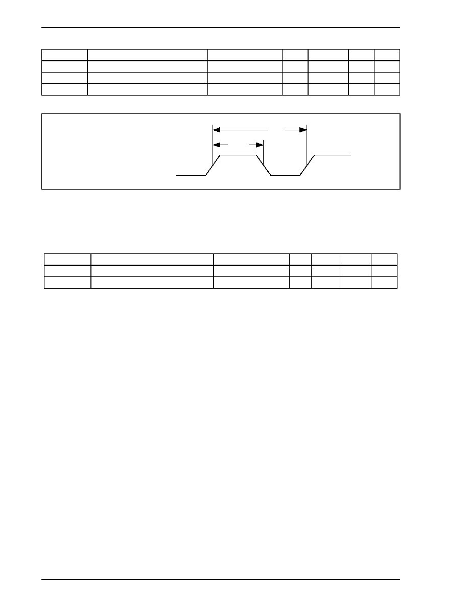
3-4
Electrical Specifications
&+,36
Æ
69000 Databook
Subject to Change Without Notice
Revision 1.3 8/31/98
Table 3-7: AC Timing Characteristics - Reference Clock
Figure 3-2: Reference Clock Timing
Table 3-8: AC Timing Characteristics - Clock Generator
Symbol
Parameter
Notes
Min
Typical
Max
Units
F
REF
Reference Frequency
1
14.31818
60
MHz
T
REF
Reference Clock Period
16.6
69.84128
1000
ns
T
HI
/T
REF
Reference Clock Duty Cycle
40
≠
60
%
Symbol
Parameter
Notes
Min
Typical
Max
Units
F
DCLK
DCLK Frequency
≠
≠
135
MHz
F
MCLK
MCLK Frequency
≠
≠
83
MHz
R eference C lo ck Inp ut
T
H I
T
R E F

Electrical Specifications
3-5
&+,36
Æ
69000 Databook
Subject to Change Without Notice
Revision 1.3 8/31/98
Table 3-9: AC Timing Characteristics - Reset
Note 1: This parameter includes time for internal voltage stabilization of all sections of the chip, startup and
stabilization of the internal clock synthesizer, and setting of all internal logic to a known state.
Note 2: This parameter includes time for the internal clock synthesizer to reset to its default frequency and
time to set all internal logic to a known state. It assumes power is stable and the internal clock
synthesizer is already operating at some stable frequency.
Note 3: This parameter specifies the setup time to latch reliably the state of the configuration bits. Changes
in some configuration bits may take longer to stabilize inside the chip (such as internal clock
synthesizer-related bits 4 and 5). The recommended configuration bit setup time is T
RES
to insure
that the chip is in a completely stable state when Reset goes inactive.
Figure 3-3: Reset Timing
Symbol Parameter
Notes
Min
Max
Units
T
IPR
Reset Inactive from Power Stable
See Note 1
1
≠
ms
T
ORS
Reset Inactive from Ext. Osc. Stable
0
≠
ms
T
RES
Minimum Reset Pulse Width
See Note 2
1
≠
ms
T
STR
Reset Inactive from Standby Inactive
RESET# is ignored in Standby Mode
2
≠
ms
T
RSR
Reset Rise Time
measured 0.1Vcc to 0.9Vcc
≠
20
ns
T
RSO
Reset Active to Output Float Delay
≠
40
ns
T
CSU
Configuration Setup Time
See Note 3
20
≠
ns
T
CHD
Configuration Hold Time
5
≠
ns
C o n fig u ra tio n
In p u ts C F G 0 -1 5
T
R SR
T
R SR
T
R SO
T
C HD
T
R ES
S TA B LE
T
O RS
T
IP R
T
S TR
T
C SU
T
C SU
T
C HD
S T N D B Y #
1 4 .3 1 8 M H z
V
C C
R E S E T #
B u s O u tp u t P in s
Initial Po wer-Up R eset
Reset w ith Chip O perating
and Po wer Stable

3-6
Electrical Specifications
&+,36
Æ
69000 Databook
Subject to Change Without Notice
Revision 1.3 8/31/98
Table 3-10: AC Timing Characteristics - PCI Bus Frame (CLK=33MHz)
Figure 3-4: PCI Bus Frame Timing
Symbol
Parameter
Notes
Min
Max
Units
T
FRS
FRAME# Setup to CLK
7
≠
ns
T
CMS
C/BE#[3:0] (Bus CMD) Setup to CLK
7
≠
ns
T
CMH
C/BE#[3:0] (Bus CMD) Hold from CLK
0
≠
ns
T
BES
C/BE#[3:0] (Byte Enable) Setup to CLK
7
≠
ns
T
BEH
C/BE#[3:0] (Byte Enable) Hold from CLK
0
≠
ns
T
ADS
AD[31:0] (Address) Setup to CLK
7
≠
ns
T
ADH
AD[31:0] (Address) Hold from CLK
0
≠
ns
T
DAS
AD[31:0] (Data) Setup to CLK
7
≠
ns
T
DAH
AD[31:0] (Data) Hold from CLK
0
≠
ns
T
DAD
AD[31:0] (Data) Valid from CLK
2
11
ns
T
TZH
TRDY# High Z to High from CLK
2
11
ns
T
THL
TRDY# Active from CLK
2
11
ns
T
TLH
TRDY# Inactive from CLK
2
11
ns
T
THZ
TRDY# High before High Z
1
≠
CLK
T
DZL
DEVSEL# Active from CLK
2
11
ns
T
DLH
DEVSEL# Inactive from CLK
2
11
ns
T
DHZ
DEVSEL# High before High Z
1
≠
CLK
T
ISC
IRDY# Setup to CLK
7
≠
ns
T
IHC
IRDY# Hold from CLK
0
≠
ns
C L K
F R A M E #
C /B E # [3 :0 ]
R e a d
A D [3 1 : 0 ]
W r ite
A D [3 1 : 0 ]
T R D Y #
IR D Y #
D E V S E L #
H i - Z
H i - Z
H i - Z
H i - Z
H i - Z
H i - Z
H i - Z
1
2
3
4
T
F R S
T
C M S
T
C M H
T
B E S
T
A D S
T
A D H
T
A D S
T
A D H
B u s
T u r n a r o u n d
B u s
T u r n a r o u n d
B u s
T u r n a r o u n d
T
T Z H
T
D Z L
R e a d
T u r n a r o u n d
B y te E n a b le s
B y te E n a b le s
T
B E H
T
D A D
T
D A S
T
D A H
T
T H L
T
T L H
T
T H Z
T
IS C
T
IH C
T
D L H
T
D H Z
B u s
T u r n a r o u n d
B u s
T u r n a r o u n d
B u s
T u r n a r o u n d
B u s
T u r n a r o u n d
H i - Z
H i - Z
H i - Z
H i - Z
H i - Z
H i - Z
H i - Z
R e a d D a ta
W r ite D a ta
W r ite D a ta
T
D A H
A d d r e s s
C o m m a n d
A d d r e s s
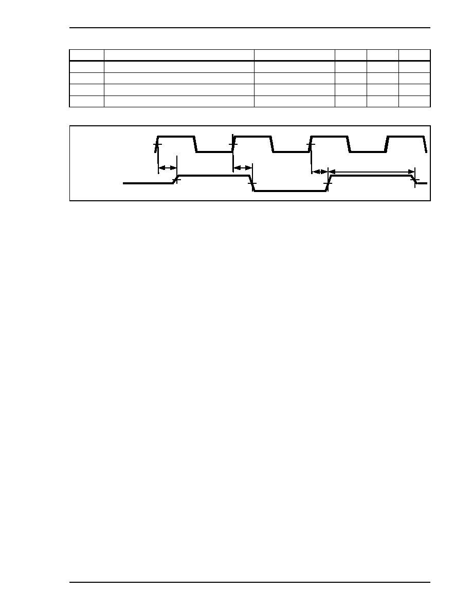
Electrical Specifications
3-7
&+,36
Æ
69000 Databook
Subject to Change Without Notice
Revision 1.3 8/31/98
Table 3-11: AC Timing Characteristics - PCI Bus Stop (CLK=33MHz)
Figure 3-5: PCI Bus Stop Timing
Symbol
Parameter
Notes
Min
Max
Units
T
SZH
STOP# High Z to High from CLK
2
11
ns
T
SHL
STOP# Active from CLK
2
11
ns
T
SLH
STOP# Inactive from CLK
2
11
ns
T
SHZ
STOP# High before High Z
1
≠
CLK
H ig h Z
C LK
S T O P #
T
S Z H
T
S H L
T
S LH
T
S H Z

3-8
Electrical Specifications
&+,36
Æ
69000 Databook
Subject to Change Without Notice
Revision 1.3 8/31/98
Table 3-12: AC Timing Characteristics BIOS ROM
Note:
PCI BIOS ROM timing is derived from the 33 MHz PCI bus clock. AGP BIOS ROM timing is derived
from the 66 MHz AGP bus clock. Timing sequences are fixed assuming the use of widely-available,
low-cost, typical industry-standard EPROMs. Timing specifications and performance of BIOS ROM
memory accesses are non-critical since PCI/AGP BIOS ROM data is always shadowed into high-
speed system memory prior to execution of BIOS code.
Figure 3-6: BIOS ROM Timing
PCI:
AGP:
Symbol
Parameter
Min
Max
Min
Max
Units
T
ROE
ROMOE# Active from CLK
≠
40
≠
20
ns
T
ROM
Slowest Permissible BIOS ROM Access Speed
≠
150
≠
75
ns
C L K
F R A M E #
A D
R O M O E #
R O M A
T R D Y #
R O M A ddr
T
R O E
Byte 0 Add r
Byte 1 Add r
Byte 2 Add r
Byte 3 Add r
D ata Valid

Electrical Specifications
3-9
&+,36
Æ
69000 Databook
Subject to Change Without Notice
Revision 1.3 8/31/98
Table 3-13: AC Timing Characteristics - Video Data Port
Figure 3-7: Video Data Port Timing
Symbol
Parameter
Notes
Min
Max
Units
T
VPS
VP0 - VP15 (Incoming Data) Setup
5
≠
ns
T
VPH
VP0 - VP15 (Incoming Data) Hold
3
≠
ns
T
HRS
HREF (Incoming HS) Setup
5
≠
ns
T
HRH
HREF (Incoming HS) Hold
In ZV-Port Mode
3
≠
ns
T
VRS
VREF (Incoming VS) Setup
5
≠
ns
T
VRH
VREF (Incoming VS) Hold
3
≠
ns
F
VCLK
VCLK Frequency (T
VCLK
is VCLK period)
10
33
MHz
VCLK Duty Cycle
40
60
%
V C LK
V P 0 -V P 1 5
H R E F
V R E F
T
V C L K
T
V P S
T
H R S
T
V R S
T
V P H
T
H R H
T
V R H

3-10
Electrical Specifications
&+,36
Æ
69000 Databook
Subject to Change Without Notice
Revision 1.3 8/31/98
Table 3-14: AC Timing Characteristics - Panel Output Timing
Note:
AC Timing is valid when max output loading=25pF.
Figure 3-8: Panel Output Timing
Symbol
Parameter
Signaling
Min
Max
Units
T
SCLK
SHFCLK cycle time
15
≠
ns
T
DOVD
DE and P[35:0] Output Valid Delay
Measured
-3
4
ns
T
COVD
LP and FLM Output Valid Delay
at 0.4V
CC
-3
3
ns
SHFCLK Duty Cycle
40
60
%
T
S L K
T
D O V D
T
C O V D
S H F C L K
D E , P [2 3 ..0 ]
L P , F L M

Electrical Specifications
3-11
&+,36
Æ
69000 Databook
Subject to Change Without Notice
Revision 1.3 8/31/98
Table 3-15: AC Timing Characteristics - A.G.P. 1x AC Timing Parameters
Note:
1 - AC Timing is valid when max output loading = 10 pF per the Intel Accelerated Graphics Port
Interface Specification Revision 2.0, however, actual test load capacitance may vary from the max
output loading of 10 pF.
Symbol
Parameter Output Timing
Min
Max
Notes
T
DAD
AD[31:0] (Data) Valid from CLK
1ns
6ns
1
T
TZH
TRDY# High Z to High from CLK
1ns
6ns
1
T
THL
TRDY# Active from CLK
1ns
5.5ns
1
T
TLH
TRDY# Inactive from CLK
1ns
5.5ns
1
T
THZ
TRDY High before High Z
-
14ns
T
DZL
DEVSEL# Active from CLK
1ns
5.5ns
1
T
DLH
DEVSEL# Inactive from CLK
1ns
5.5ns
1
T
DHZ
DEVSEL# High before High Z
-
14ns
T
SZH
STOP# High Z to High from CLK
1ns
6ns
1
T
SHL
STOP# Active from CLK
1ns
5.5ns
1
T
SLH
STOP# Inactive from CLK
1ns
5.5ns
1
T
SHZ
STOP# High before High Z
-
14ns
Address/Read/Write Cycle Input Timing
T
ADS
Address Setup to CLK
6ns
-
T
ADH
Address Hold from CLK
0ns
-

3-12
Electrical Specifications
&+,36
Æ
69000 Databook
Subject to Change Without Notice
Revision 1.3 8/31/98

Mechanical Specifications
4-1
&+,36
Æ
69000
Databook
Subject to Change Without Notice
Revision 1.3 8/31/98
Chapter 4
Mechanical Specifications
Figure 4-1: 256+16-Contact Ball Grid Array
1.27mm
(0.0500")
BSC
1.435mm
(0.0565")
1.53mm
(0.0602")
max
27
±
0.
1 m
m
(
1
.
0
6
3
±
0.
00
4")
Bottom View
Diameter:
0.760 ± 0.16
(0.0299 ± 0.0023)
256 +16 places
27 ± 0.1 mm (1.063 ± 0.004")
Y W V U T R P N M L K J H G F E D C B A
20
19
18
17
16
15
14
13
12
11
10
9
8
7
6
5
4
3
2
1
1.27mm
(0.0500")
BSC
1.435mm
(0.0565")
2.2mm max
(0.087")
27
±
0.
1 m
m
(
1
.
0
6
3
±
0.
00
4")
Top View
27 ± 0.1 mm (1.063 ± 0.004")
20
19
18
17
16
15
14
13
12
11
10
9
8
7
6
5
4
3
2
1
A B C D E F G H J K L M N P R T U V W Y
Diameter:
0.760 ± 0.16
(0.0299 ± 0.0023)
256 +16 places

4-2
Mechanical Specifications
&+,36
Æ
69000
Databook
Subject to Change Without Notice
Revision 1.3 8/31/98
Figure 4-2: 256 Ball - Mini Ball Grid Array
A
B
C
D
E
F
G
H
J
K
L
M
N
P
R
T
1 7.00 +/- .20 m m
16 15 1 4 1 3 12 11 1 0 9 8 7 6 5 4 3 2 1
1 .0 0 +/-
0 .1 0m m
1 5.0 B S C
1 .0 0 +/-
0 .1 0m m
1 5.0 B S C
1 7.00 +/- .20 m m
1 .4 5 + /- .1 0m m
0 .4 0 + /- .0 5m m

I/O and Memory Address Maps
5-1
&+,36
Æ
69000 Databook
Subject to Change Without Notice
Revision 1.3 8/31/98
Chapter 5
I/O and Memory Address Maps
An extensive set of registers normally controls the graphics system. These registers are a combination of
registers defined by IBM when the Video Graphics Array (VGA) was first introduced, and others that have
been added to support graphics modes that have color depths, resolutions, and hardware acceleration
features that go well beyond the original VGA standard. This chapter provides an overview of the address
locations and sub-addressing mechanisms used to access the various registers and the frame buffer of this
graphics controller.
Some of the registers are directly accessible at various I/O addresses. They may be read-only or write-only,
and some must be read from and written to at different I/O addresses. Most of the other registers are
accessed through a sub-addressing arrangement. The index of the desired register is written to an index
register, and then the desired register may be read from or written to through a data port. Almost all of these
sub-addressed registers are both readable and writable. Still other registers are directly accessible at
various memory addresses and here too, almost all of these registers are both readable and writable.
VGA-Compatible Address Map
Part of the VGA standard requires the VGA graphics system to take the place of either the IBM Monochrome
Display and Printer Adapter (either MDPA or MDA) or the IBM Color Graphics Adapter (CGA). This was
also the case with the IBM Enhanced Graphics Adapter (EGA), VGA's predecessor. The MDA has registers
at I/O addresses 3B4-3B5 and 3BA, and a character buffer (not a frame buffer -- the MDA is a text-only
device) within the memory address range of B0000-B7FFF. The CGA has registers within I/O addresses
3D4-3D5 and 3DA-3DC, and a frame buffer (for either text or graphics) within the memory address range
of B8000-BFFFF.
The VGA standard introduced numerous modes with features that went beyond those originally provided by
either MDA or CGA. To do this, the VGA standard introduced many additional registers at locations in the
3C0-3CF I/O address range, and an additional frame buffer memory space in the A0000-AFFFF memory
address range through which the frame buffer could be accessed. This additional memory address region
is a 64KB "port-hole" by which the standard 256KB VGA frame buffer is accessed. Either different 64KB
portions of this frame buffer are swapped or "paged" in and out of this port-hole as a way of gaining access
to all of it, or this frame buffer can be reorganized into "planes" that can be made selectively or even
simultaneously accessible though this port-hole as part of a mechanism to enable bit-wise graphics color
manipulation. This was done as part of the VGA standard partly because of the shortage of available
addresses in the first 1MB of memory address space in PC-standard systems.
If a PC with a VGA graphics system does not have either an MDA display system or a CGA graphics system,
the VGA BIOS will initialize the VGA graphics system to take the place of either an MDA if a monochrome
display is attached to the VGA, or of a CGA if a color display is attached. However, if a PC with a VGA
graphics system also has an MDA display system, the VGA is initialized to take the place of a CGA,
regardless of the type of monitor attached to the VGA in order to avoid conflicts with the MDA. Likewise, if
a PC with a VGA graphics system also has a CGA graphics system, the VGA is initialized to take the place
of an MDA, regardless of the type of monitor attached to the VGA. The VGA standard does not allow a
system to have both an MDA display system and a CGA graphics system in the same PC along with a VGA
graphics system.

5-2
I/O and Memory Address Maps
&+,36
Æ
69000 Databook
Subject to Change Without Notice
Revision 1.3 8/31/98
Address Maps for Going Beyond VGA
This graphics controller improves upon VGA by providing additional features that are used through
numerous additional registers. Many of these additional registers are simply added to the sub-addressing
schemes already defined in the VGA standard, while others are added through sub-addressing schemes
using additional I/O address locations 3D0-3D3 and 3D6-3D7. This graphics controller also provides for the
memory-mapping of both the standard VGA and these additional registers alongside I/O-mapping. All of
the registers that are accessible via I/O addresses 3B0 through 3DF are also accessible at offsets 400760
through 4007BF from the starting address of the upper memory space. Still more of these additional
registers are 32 bits wide and for performance reasons are accessible exclusively at other offsets from the
starting address of the upper memory space.
This graphics controller also supports 1 or more megabytes of frame buffer memory -- far larger than VGA's
standard complement of 256KB. As an improvement upon the VGA standard frame buffer port-hole, this
graphics controller also maps the entire frame buffer into part of a single contiguous memory space at a
programmable location, providing what is called "linear" access to the frame buffer. The size of this memory
space is 16MB (however, the frame buffer does not fill this entire memory space), and the base address is
set through a PCI configuration register.
Most aspects of the host interface of this graphics controller are configured through a set of built-in PCI-
compliant setup registers. The system logic accesses these registers through standard PCI configuration
read and write cycles. Therefore, the exact location of the PCI configuration registers for this graphics
controller, as well as any other PCI device in the system I/O or memory address space depends on the
system logic design and the system software that configures the system.

I/O and Memory Address Maps
5-3
&+,36
Æ
69000 Databook
Subject to Change Without Notice
Revision 1.3 8/31/98
PCI Configuration Registers
Configuration
Space Offset
Name
Function
Access
Bits
00
VENDID
Vendor ID
read-only
16
02
DEVID
Device ID
read-only
16
04
DEVCTL
Device Control
read/clear
16
06
DEVSTAT
Device Status
read-only
16
08
REV
Revision ID
read-only
8
09
PRG
Programming Interface
read-only
8
0A
SUB
Sub-Class Code
read-only
8
0B
BASE
Base Class Code
read-only
8
0C
Reserved (Cache Line Size)
--
8
0D
Reserved (Latency Timer)
--
8
0E
Reserved (Header Type)
--
8
0F
Reserved (Built-In-Self-Test)
--
8
10
MBASE
Memory Base Address
read/write
32
14
Reserved (Base Address)
--
32
18
Reserved (Base Address)
--
32
1C
Reserved (Base Address)
--
32
20
Reserved (Base Address)
--
32
24
Reserved (Base Address)
--
32
28
Reserved
--
32
2C
SUBVENDID
Subsystem Vendor ID
read-only
16
2E
SUBDEVID
Subsystem Device ID
read-only
16
30
RBASE
ROM Base Address
read/write
32
34
Reserved
--
32
38
Reserved
--
32
3C
INTLINE
Interrupt Line
read/write
8
3D
INTPIN
Interrupt Pin
read-only
8
3E
Reserved (Minimum Grant)
--
8
3F
Reserved (Maximum Latency)
--
8
40 to 6B
6C
SUBVENDSET
Subsystem Vendor ID Set
read/write
16
6E
SUBDEVSET
Subsystem Device ID Set
read/write
16
6F to FF

5-4
I/O and Memory Address Maps
&+,36
Æ
69000 Databook
Subject to Change Without Notice
Revision 1.3 8/31/98
I/O and Sub-Addressed Register Map
I/O Address
Memory
Offset
Read
Write
3B0-3B3
3B4
0x400768
CRTC Index (MDA Emulation)
3B5
0x400769
CRTC Data Port (MDA Emulation)
3B6-3B9
3BA
0x400774
Input Status Register 1 (ST01)
(MDA Emulation)
Feature Control Register (FCR)
(MDA Emulation)
3BB-3BF
3C0
0x400780
Attribute Controller Index
Attribute Controller Index and Data Port
3C1
0x400781
Attribute Controller Data Port
Alternate Attribute Controller Data Port
3C2
0x400784
Input Status Register 0 (ST00)
Misc. Output Register (MSR)
3C3
3C4
0x400788
Sequencer Index
3C5
0x400789
Sequencer Data Port
3C6
0x40078C
Color Palette Mask
3C7
0x40078D
Color Palette State
Color Palette Read Mode Index
3C8
0x400790
Color Palette Write Mode Index
3C9
0x400791
Color Palette Data Port
3CA
0x400794
Feature Control Register (FCR)
3CB
3CC
0x400798
Misc. Output Register (MSR)
3CD
3CE
0x40079C
Graphics Controller Index
3CF
0x40079D
Graphics Controller Data Port
3D0
0x4007A0
Flat Panel Extensions Index
3D1
0x4007A1
Flat Panel Extensions Data Port
3D2
0x4007A4
Multimedia Extensions Index
3D3
0x4007A5
Multimedia Extensions Data Port
3D4
0x4007A8
CRTC Index (CGA Emulation)
3D5
0x4007A9
CRTC Data Port (CGA Emulation)
3D6
0x4007AC
Configuration Extensions Index
3D7
0x4007AD
Configuration Extensions Data Port
3D8-3D9
3DA
0x4007B4
Input Status Register 1 (ST01)
(CGA Emulation)
Feature Control Register (FCR)
(CGA Emulation)
3DB-3DF

I/O and Memory Address Maps
5-5
&+,36
Æ
69000 Databook
Subject to Change Without Notice
Revision 1.3 8/31/98
Sub-Addressing Indexes and Data Ports
Index Port
Addresses
Data Port
Addresses
Register
Group
Name
Function
I/O 3C0
Mem 0x400780
I/O 3C0/3C1
Mem 0x400780/781
Attribute
Controller
AR0-14
VGA Attributes Control
I/O 3C4
Mem 0x400788
I/O 3C5
Mem 0x400789
Sequencer
SR0-7
VGA Sequencer Control
I/O 3CE
Mem 0x40079C
I/O 3CF
Mem 0x40079D
Graphics
Controller
GR0-8
VGA Data Path Control
I/O 3D0
Mem 0x4007A0
I/O 3D1
Mem 0x4007A1
Flat Panel
FR00-1F
FR20-2F
FR30-3F
FR40-47
FR48-4F
FR50-5F
FR60-6F
FR70-7F
General Panel Control
Horizontal Panel Timing
Vertical Panel Timing
Horizontal Compensation
Vertical Compensation
--
--
--
I/O 3D2
Mem 0x4007A4
I/O 3D3
Mem 0x4007A5
Multimedia
MR00-1F
MR20-3F
MR40-5F
MR60-7F
Acquisition/Capture
Playback Window Display
Color Key
--
I/O 3B4/3D4
Mem 0x400768/7A8
I/O 3B5/3D5
Mem 0x400769/7A9
CRTC
CR00-2F
CR30-3F
CR40-4F
CR50-5F
CR60-6F
CR70-7F
CR80-FF
Basic Display Control
Timing Extension Bits
Address Extension Bits
Display Overlay
--
Interlace Control
--
I/O 3D6
Mem 0x4007AC
I/O 3D7
Mem 0x4007AD
Extension
Registers
XR00-0F
XR10-1F
XR20-2F
XR30-3F
XR40-4F
XR50-5F
XR60-6F
XR70-7F
XR80-8F
XR90-9F
XRA0-AF
XRB0-BF
XRC0-CF
XRD0-DF
XRE0-EF
XRF0-FF
General Configuration
--
Graphics Engine Configuration
--
Memory Configuration
--
Pin Control
Configuration Pins
Pixel Pipeline
--
Hardware Cursor
--
Clock Control
Power Management
Software Flags
Hardware Testing

5-6
I/O and Memory Address Maps
&+,36
Æ
69000 Databook
Subject to Change Without Notice
Revision 1.3 8/31/98
Lower Memory Map
Address Range
Function
Size in Bytes
A0000-AFFFF
VGA Frame Buffer
64KB
B0000-B7FFF
MDA Emulation Character Buffer
32KB
B8000-BFFFF
CGA Emulation Frame Buffer
32KB
C0000-C7FFF
or
C0000 up to CFFFF
VGA BIOS ROM
32KB
or
Larger (up to 64KB)

I/O and Memory Address Maps
5-7
&+,36
Æ
69000 Databook
Subject to Change Without Notice
Revision 1.3 8/31/98
Upper Memory Map
Size
Memory Offset
Function
2MB
0x000000 to
0x1FFFFF
Linear Frame Buffer
(Little-Endian)
2MB
0x200000 to
0x3FFFFF
64 Bytes
0x400000 to
0x40003F
BitBLT Registers
(Little-Endian)
1472
Bytes
0x400040 to
0x4005FF
2KB
64 Bytes
0x400600 to
0x40063F
ER Registers
(Little-Endian)
192 Bytes
0x400640 to
0x4006FF
8MB
4MB
256 Bytes
0x400700 to
0x4007FF
VGA and Sub-Addressed Registers
(Little-Endian)
62KB
0x400800 to
0x40FFFF
16MB
64KB
0x410000 to
0x41FFFF
BitBLT Data Port
(Little-Endian)
3968KB
0x420000 to
0x7FFFFF
2MB
0x800000 to
0x9FFFFF
Linear Frame Buffer
(Big-Endian)
2MB
0xA00000 to
0xBFFFFF
8MB
64KB
0xC00000 to
0xC0FFFF
4MB
64KB
0xC10000 to
0xC1FFFF
BitBLT Data Port
(Big-Endian)
3968KB
0xC20000 to
0xFFFFFF

5-8
I/O and Memory Address Maps
&+,36
Æ
69000 Databook
Subject to Change Without Notice
Revision 1.3 8/31/98
Register Summaries
6-1
&+,36
Æ
69000 Databook
Subject to Change Without Notice
Revision 1.3 8/31/98
Chapter 6
Register Summaries
Table 6-1 PCI Configuration Registers
Table 6-2: General Control & Status Registers
Configuration
Space Offset
Name
Register Function
Access
Bits
00
VENDID
Vendor ID Register
read-only
16
02
DEVID
Device ID Register
read-only
16
04
DEVCTL
Device Control Register
read/clear
16
06
DEVSTAT
Device Status Register
read-only
16
08
REV
Revision ID Register
read-only
8
09
PRG
Programming Interface Register
read-only
8
0A
SUB
Sub-Class Code Register
read-only
8
0B
BASE
Base Class Code Register
read-only
8
0C
Reserved (Cache Line Size)
--
8
0D
Reserved (Latency Timer)
--
8
0E
Reserved (Header Type)
--
8
0F
Reserved (Built-In-Self-Test)
--
8
10
MBASE
Memory Base Address Register
read/write
32
14
Reserved (Base Address)
--
32
18
Reserved (Base Address)
--
32
1C
Reserved (Base Address)
--
32
20
Reserved (Base Address)
--
32
24
Reserved (Base Address)
--
32
28
Reserved
--
32
2C
SUBVENDID
Subsystem Vendor ID Register
read-only
16
2E
SUBDEVID
Subsystem Device ID Register
read-only
16
30
RBASE
ROM Base Address Register
read/write
32
34
Reserved
--
32
38
Reserved
--
32
3C
INTLINE
Interrupt Line Register
read/write
8
3D
INTPIN
Interrupt Pin Register
read-only
8
3E
Reserved (Minimum Grant)
--
8
3F
Reserved (Maximum Latency)
--
8
40 to 6B
6C
SUBVENDSET
Subsystem Vendor ID Set Register
read/write
16
6E
SUBDEVSET
Subsystem Device ID Set Register
read/write
16
6F to FF
Name
Register Function
Read
Write
ST00
VGA Input Status Register 0
3C2
--
ST01
VGA Input Status Register 1
3BA/3DA
--
FCR
VGA Feature Control Register
3CA
3BA/3DA
MSR
VGA Miscellaneous Output Register
3CC
3C2

6-2
Register Summaries
&+,36
Æ
69000 Databook
Subject to Change Without Notice
Revision 1.3 8/31/98
Table 6-3: CRT Controller Registers
Note:
CR00-CR22 are standard VGA registers -- all other CR registers are CHIPS extensions.
Name
Register Function
Access
3B5/3D5
Index Value
3B4/3D4 (CRX)
CR00
Horizontal Total Register
read/write
00h
CR01
Horizontal Display Enable End Register
read/write
01h
CR02
Horizontal Blanking Start Register
read/write
02h
CR03
Horizontal Blanking End Register
read/write
03h
CR04
Horizontal Sync Start Register
read/write
04h
CR05
Horizontal Sync End Register
read/write
05h
CR06
Vertical Total Register
read/write
06h
CR07
Overflow Register
read/write
07h
CR08
Preset Row Scan Register
read/write
08h
CR09
Maximum Scanline Register
read/write
09h
CR0A
Text Cursor Start Scanline Register
read/write
0Ah
CR0B
Text Cursor End Scanline Register
read/write
0Bh
CR0C
Start Address High Register
read/write
0Ch
CR0D
Start Address Low Register
read/write
0Dh
CR0E
Text Cursor Location High Register
read/write
0Eh
CR0F
Text Cursor Location Low Register
read/write
0Fh
CR10
Vertical Sync Start Register
read/write
10h
CR11
Vertical Sync End Register
read/write
11h
CR12
Vertical Display Enable End Register
read/write
12h
CR13
Offset Register
read/write
13h
CR14
Underline Row Register
read/write
14h
CR15
Vertical Blanking Start Register
read/write
15h
CR16
Vertical Blanking End Register
read/write
16h
CR17
CRT Mode Control Register
read/write
17h
CR18
Line Compare Register
read/write
18h
CR22
Memory Read Latch Data Register
read-only
22h
CR30
Extended Vertical Total Register
read/write
30h
CR31
Extended Vertical Display End Register
read/write
31h
CR32
Extended Vertical Sync Start Register
read/write
32h
CR33
Extended Vertical Blanking Start Register
read/write
33h
CR38
Extended Horizontal Total Register
read/write
38h
CR3C
Extended Horizontal Blanking End Register
read/write
3Ch
CR40
Extended Start Address Register
read/write
40h
CR41
Extended Offset Register
read/write
41h
CR70
Interlace Control Register
read/write
70h
CR71
NTSC/PAL Video Output Control Register
read/write
71h
CR72
NTSC/PAL Horizontal Serration 1 Start Register
read/write
72h
CR73
NTSC/PAL Horizontal Serration 2 Start Register
read/write
73h
CR74
NTSC/PAL Horizontal Pulse Width Register
read/write
74h
CR75
NTSC/PAL Filtering Burst Read Length Register
read/write
75h
CR76
NTSC/PAL Filtering Burst Read Quantity Register
read/write
76h
CR77
NTSC/PAL Filtering Control Register
read/write
77h
CR78
NTSC/PAL Vertical Reduction Register
read/write
78h
CR79
NTSC/PAL Pixel Resolution Fine Adjust Register
read/write
79h

Register Summaries
6-3
&+,36
Æ
69000 Databook
Subject to Change Without Notice
Revision 1.3 8/31/98
Table 6-4: Sequencer Registers
Table 6-5: Graphics Controller Registers
Table 6-6: Attribute Controller Registers
Table 6-7: Palette Registers
Name
Register Function
Access
(via 3C5)
Index Value
In 3C4 (SRX)
SR00
Reset Register
read/write
00
SR01
Clocking Mode Register
read/write
01
SR02
Map Mask Register
read/write
02
SR03
Character Map Select Register
read/write
03
SR04
Memory Mode Register
read/write
04
SR07
Horizontal Character Counter Reset Register
read/write
07
Name
Register Function
Access
(via 3CF)
Index Value
In 3CE (GRX)
GR00
Set/Reset Register
read/write
00h
GR01
Enable Set/Reset Register
read/write
01h
GR02
Color Compare Register
read/write
02h
GR03
Data Rotate Register
read/write
03h
GR04
Read Map Select Register
read/write
04h
GR05
Graphics Mode Register
read/write
05h
GR06
Miscellaneous Register
read/write
06h
GR07
Color Don't Care Register
read/write
07h
GR08
Bit Mask Register
read/write
08h
Name
Register Function
Access
(via 3C0/3C1)
Index Value
In 3C0 (ARX)
AR00-AR0F
Color Data Registers
read/write
00-0F
AR10
Mode Control Register
read/write
10
AR11
Overscan Color Register
read/write
11
AR12
Memory Plane Enable Register
read/write
12
AR13
Horizontal Pixel Panning Register
read/write
13
AR14
Color Select Register
read/write
14
Name
Register Function
Access
(via 3C9)
I/O Address
In 3C7/3C8
PALMASK
Palette Mask Register
read/write
3C6h
PALSTATE
Palette State Register
read-only
3C7h
PALRX
Palette Read Index Register
write-only
3C7h
PALWX
Palette Write Index Register
read/write
3C8h
PALDATA
Palette Data Register
read/write
3C9h

6-4
Register Summaries
&+,36
Æ
69000 Databook
Subject to Change Without Notice
Revision 1.3 8/31/98
Table 6-8: Extension Registers
Name
Register Function
Access
(via 3D7)
Index Value
In 3D6 (XRX)
XR00
Vendor ID Low Register
read-only
00h
XR01
Vendor ID High Register
read-only
01h
XR02
Device ID Low Register
read-only
02h
XR03
Device ID High Register
read-only
03h
XR04
Revision ID Register
read-only
04h
XR05
Linear Base Address Low Register
read-only
05h
XR06
Linear Base Address High Register
read-only
06h
XR08
Host Bus Configuration Register
read-only
08h
XR09
I/O Control Register
read/write
09h
XR0A
Frame Buffer Mapping Register
read/write
0Ah
XR0B
PCI Burst Write Support Register
read/write
0Bh
XR0E
Frame Buffer Page Select Register
read/write
0Eh
XR20
BitBLT Configuration Register
read/write
20h
XR40
Memory Access Control Register
read/write
40h
XR41-XR4F
Memory Configuration Registers
read/write
41h-4Fh
XR60
Video Pin Control Register
read/write
60h
XR61
DPMS Sync Control Register
read/write
61h
XR62
GPIO Pin Control Register
read/write
62h
XR63
GPIO Pin Data Register
read/write
63h
XR67
Pin Tri-State Control Register
read/write
67h
XR70
Configuration Pins 0 Register
read-only
70h
XR71
Configuration Pins 1 Register
read-only
71h
XR80
Pixel Pipeline Configuration 0 Register
read/write
80h
XR81
Pixel Pipeline Configuration 1 Register
read/write
81h
XR82
Pixel Pipeline Configuration 2 Register
read/write
82h

Register Summaries
6-5
&+,36
Æ
69000 Databook
Subject to Change Without Notice
Revision 1.3 8/31/98
Table 6-8: Extension Registers (continued)
Name
Register Function
Access Via
Port 3D7
Index Value
Port 3D6 (XRX)
XRA0
Cursor 1 Control Register
read/write
A0h
XRA1
Cursor 1 Vertical Extension Register
read/write
A1h
XRA2
Cursor 1 Base Address Low Register
read/write
A2h
XRA3
Cursor 1 Base Address High Register
read/write
A3h
XRA4
Cursor 1 X-Position Low Register
read/write
A4h
XRA5
Cursor 1 X-Position High Register
read/write
A5h
XRA6
Cursor 1 Y-Position Low Register
read/write
A6h
XRA7
Cursor 1 Y-Position High Register
read/write
A7h
XRA8
Cursor 2 Control Register
read/write
A8h
XRA9
Cursor 2 Vertical Extension Register
read/write
A9h
XRAA
Cursor 2 Base Address Low Register
read/write
AAh
XRAB
Cursor 2 Base Address High Register
read/write
ABh
XRAC
Cursor 2 X-Position Low Register
read/write
ACh
XRAD
Cursor 2 X-Position High Register
read/write
ADh
XRAE
Cursor 2 Y-Position Low Register
read/write
AEh
XRAF
Cursor 2 Y-Position High Register
read/write
AFh
XRC0
Dot Clock 0 VCO M-Divisor Low Register
read/write
C0h
XRC1
Dot Clock 0 VCO N-Divisor Low Register
read/write
C1h
XRC2
Dot Clock 0 VCO M/N-Divisor High Register
read/write
C2h
XRC3
Dot Clock 0 Divisor Select Register
read/write
C3h
XRC4
Dot Clock 1 VCO M-Divisor Low Register
read/write
C4h
XRC5
Dot Clock 1 VCO N-Divisor Low Register
read/write
C5h
XRC6
Dot Clock 1 VCO M/N-Divisor High Register
read/write
C6h
XRC7
Dot Clock 1 Divisor Select Register
read/write
C7h
XRC8
Dot Clock 2 VCO M-Divisor Low Register
read/write
C8h
XRC9
Dot Clock 2 VCO N-Divisor Low Register
read/write
C9h
XRCA
Dot Clock 2 VCO M/N-Divisor High Register
read/write
CAh
XRCB
Dot Clock 2 Divisor Select Register
read/write
CBh
XRCC
Memory Clock VCO M-Divisor Register
read/write
CCh
XRCD
Memory Clock VCO N-Divisor Register
read/write
CDh
XRCE
Memory Clock VCO Divisor Select Register
read/write
CEh
XRCF
Clock Configuration Register
read/write
CFh
XRD0
Powerdown Control Register
read/write
D0h
XRD1
Power Conservation Control Register
read/write
D1h
XRD2
2KHz Down Counter Register
read-only
D2h
XRE0-XRE9
Software Flag Registers
read/write
E0h-E9h
XRF8-XRFC
Test Registers
read/write
F8h-FCh

6-6
Register Summaries
&+,36
Æ
69000 Databook
Subject to Change Without Notice
Revision 1.3 8/31/98
Table 6-9: Flat Panel Registers
Name
Register Function
Access Via
Port 3D1h
Index Value
Port 3D0h
FR00
Feature Register
read-only
00h
FR01
CRT / FP Control Register
read/write
01h
FR02
FP Mode Control Register
read/write
02h
FR03
FP Dot Clock Source Register
read/write
03h
FR04
Panel Power Sequencing Delay Register
read/write
04h
FR05
Power Down Control 1 Register
read/write
05h
FR06
FP Power Down Control Register
read/write
06h
FR08
FP Pin Polarity Register
read/write
08h
FR0A
Programmable Output Drive Register
read/write
0Ah
FR0B
FP Pin Control 1 Register
read/write
0Bh
FR0C
Pin Control 2 Register
read/write
0Ch
FR0F
Activity Timer Control Register
read/write
0Fh
FR10
FP Format 0 Register
read/write
10h
FR11
FP Format 1 Register
read/write
11h
FR12
FP Format 2 Register
read/write
12h
FR13
FP Format 3 Register
read/write
13h
FR16
FRC Option Select Register
read/write
16h
FR17
Polynomial FRC Control Register
read/write
17h
FR18
FP Text Mode Control Register
read/write
18h
FR19
Blink Rate Control Register
read/write
19h
FR1A
STN-DD Buffering Control Register
read/write
1Ah
FR1E
M (ACDCLK) Control Register
read/write
1Eh
FR1F
Diagnostic Register
read/write
1Fh
FR20
FP Horizontal Panel Display Size LSB Register
read/write
20h
FR21
FP Horizontal Sync Start LSB Register
read/write
21h
FR22
FP Horizontal Sync End Register
read/write
22h
FR23
FP Horizontal Total LSB Register
read/write
23h
FR24
FP HSync (LP) Delay LSB Register
read/write
24h
FR25
FP Horizontal Overflow 1 Register
read/write
25h
FR26
FP Horizontal Overflow 2 Register
read/write
26h
FR27
FP HSync (LP) Width and Disable Register
read/write
27h
FR30
FP Vertical Panel Size LSB Register
read/write
30h
FR31
FP Vertical Sync Start LSB Register
read/write
31h
FR32
FP Vertical Sync End Register
read/write
32h
FR33
FP Vertical Total LSB Register
read/write
33h
FR34
FP VSync (FLM) Delay LSB Register
read/write
34h
FR35
FP Vertical Overflow 1 Register
read/write
35h
FR36
FP Vertical Overflow 2 Register
read/write
36h
FR37
FP VSync (FLM) Disable Register
read/write
37h
FR40
Horizontal Compensation Register
read/write
40h
FR41
Horizontal Stretching Register
read/write
41h
FR48
Vertical Compensation Register
read/write
48h
FR49-4C
Text Mode Vertical Stretching 0 MSB Registers
read/write
49h-4Ch
FR4D
Vertical Line Replication Register
read/write
4Dh
FR4E
Selective Vertical Stretching Disable Register
read/write
4Eh
FR70
TMED Red Seed Register
read/write
70h
FR71
TMED Green Seed Register
read/write
71h
FR72
TMED Blue Seed Register
read/write
72h
FR73
TMED Control Register
read/write
73h
FR74
TMED2 Shift Control Register
read/write
74h

Register Summaries
6-7
&+,36
Æ
69000 Databook
Subject to Change Without Notice
Revision 1.3 8/31/98
Table 6-10: Multimedia Registers
Name
Register Function
Access Via
3D3h
Index at 3D2h
Set to Value
MR00
Module Capability Register
read-only
00h
MR01
Secondary Capability Register
read-only
01h
MR02
Capture Control 1 Register
read/write
02h
MR03
Capture Control 2 Register
read/write
03h
MR04
Capture Control 3 Register
read/write
04h
MR05
Capture Control 4 Register
read/write
05h
MR06-08
Capture Memory Address PTR1 Register
read/write
06h - 08h
MR09-0B
Capture Memory Address PTR2 Register
read/write
09h - 0Bh
MR0C
Capture Memory Width (Span) Register
read/write
0Ch
MR0E
Capture Window X-LEFT Low Register
read/write
0Eh
MR0F
Capture Window X-LEFT High Register
read/write
0Fh
MR10
Capture Window X-RIGHT Low Register
read/write
10h
MR11
Capture Window X-RIGHT High Register
read/write
11h
MR12
Capture Window Y-TOP Low Register
read/write
12h
MR13
Capture Window Y-TOP High Register
read/write
13h
MR14
Capture Window Y-BOTTOM Low Register
read/write
14h
MR15
Capture Window Y-BOTTOM High Register
read/write
15h
MR16
H-SCALE Register
read/write
16h
MR17
V-SCALE Register
read/write
17h
MR18
Capture Frame Count Register
read/write
18h
MR1E
Playback Control 1 Register
read/write
1Eh
MR1F
Playback Control 2 Register
read/write
1Fh
MR20
Playback Control 3 Register
read/write
20h
MR21
Double Buffer Status Register
read/write
21h
MR22-24
Playback Memory Address PTR1 Register
read/write
22h - 24h
MR25-27
Playback Memory Address PTR2 Register
read/write
25h - 27h
MR28
Playback Memory Line Fetch Width Register
read/write
28h
MR2A
Playback Window X-LEFT Low Register
read/write
2Ah
MR2B
Playback Window X-LEFT High Register
read/write
2Bh
MR2C
Playback Window X-RIGHT Low Register
read/write
2Ch
MR2D
Playback Window X-RIGHT High Register
read/write
2Dh
MR2E
Playback Window Y-TOP Low Register
read/write
2Eh
MR2F
Playback Window Y-TOP High Register
read/write
2Fh
MR30
Playback Window Y-BOTTOM Low Register
read/write
30h
MR31
Playback Window Y-BOTTOM High Register
read/write
31h
MR32
H-ZOOM Register
read/write
32h
MR33
V-ZOOM Register
read/write
33h
MR34
Memory Line Out Total Register
read/write
34h
MR3C
Color Key Control 1 Register
read/write
3Ch
MR3D-3F
Color Keys Register
read/write
3Dh - 3Fh
MR40-42
Color Key Masks Register
read/write
40h - 42h
MR43
Line Count Low Register
read-only
43h
MR44
Line Count High Register
read-only
44h
6-8
Register Summaries
&+,36
Æ
69000 Databook
Subject to Change Without Notice
Revision 1.3 8/31/98
Table 6-11: BitBLT Registers
Table 6-12: Memory-mapped Wide Extension Registers
Name
Function
Access
Offset
BR00
Source and Destination Offset Register
read/write
0x400000
BR01
Pattern/Source Expansion Background Color Register
read/write
0x400004
BR02
Pattern/Source Expansion Foreground Color Register
read/write
0x400008
BR03
Monochrome Source Control Register
read/write
0x40000C
BR04
BitBLT Control Register
read/write
0x400010
BR05
Pattern Address Register
read/write
0x400014
BR06
Source Address Register
read/write
0x400018
BR07
Destination Address Register
read/write
0x40001C
BR08
Destination Width & Height Register
read/write
0x400020
BR09
Source Expansion Background Color Register
read/write
0x400024
BR0A
Source Expansion Foreground Color Register
read/write
0x400028
Name
Function
Access
Offset
ER00
Central Interrupt Control Register
read/write
0x400100
ER01
Central Interrupt Status Register
read/write
0x400104
ER03
Miscellaneous Function Register
read/write
0x40010C

PCI Configuration Registers
7-1
&+,36
Æ
69000 Databook
Subject to Change Without Notice
Revision 1.3 8/31/98
Chapter 7
PCI Configuration Registers
Table 7-1 PCI Configuration Registers
Note: The mechanism used to generate the PCI configuration read and configuration write cycles by which
these registers are accessed is system-dependent.
Configuration
Space Offset
Name
Function
Access
Bits
00
VENDID
Vendor ID Register
read-only
16
02
DEVID
Device ID Register
read-only
16
04
DEVCTL
Device Control Register
read/clear
16
06
DEVSTAT
Device Status Register
read-only
16
08
REV
Revision ID Register
read-only
8
09
PRG
Programming Interface Register
read-only
8
0A
SUB
Sub-Class Code Register
read-only
8
0B
BASE
Base Class Code Register
read-only
8
0C
Reserved (Cache Line Size)
--
8
0D
Reserved (Latency Timer)
--
8
0E
Reserved (Header Type)
--
8
0F
Reserved (Built-In-Self-Test)
--
8
10
MBASE
Memory Base Address Register
read/write
32
14
Reserved (Base Address)
--
32
18
Reserved (Base Address)
--
32
1C
Reserved (Base Address)
--
32
20
Reserved (Base Address)
--
32
24
Reserved (Base Address)
--
32
28
Reserved
--
32
2C
SUBVENDID
Subsystem Vendor ID Register
read-only
16
2E
SUBDEVID
Subsystem Device ID Register
read-only
16
30
RBASE
ROM Base Address Register
read/write
32
34
Reserved
--
32
38
Reserved
--
32
3C
INTLINE
Interrupt Line Register
read/write
8
3D
INTPIN
Interrupt Pin Register
read-only
8
3E
Reserved (Minimum Grant)
--
8
3F
Reserved (Maximum Latency)
--
8
40 to 6B
6C
SUBVENDSET
Subsystem Vendor ID Set Register
read/write
16
6E
SUBDEVSET
Subsystem Device ID Set Register
read/write
16
6F to FF

7-2
PCI Configuration Registers
&+,36
Æ
69000 Databook
Subject to Change Without Notice
Revision 1.3 8/31/98
VENDID Vendor ID Register
read-only at PCI configuration offset 00h
byte or word accessible
accessible only via PCI configuration cycles
15-0
Vendor ID
This is the vendor ID assigned to CHIPS by the PCI Special Interest group. This register always
returns the 16-bit value 102Ch (4140 decimal).
DEVID Device ID Register
read-only at PCI configuration offset 02h
byte or word accessible
accessible only via PCI configuration cycles
15-0
Device ID
This is the device ID assigned to the 69000 by CHIPS. This register always returns the 16-bit value
00C0h when read.
15
14
13
12
11
10
9
8
7
6
5
4
3
2
1
0
Vendor ID
(102Ch)
15
14
13
12
11
10
9
8
7
6
5
4
3
2
1
0
Device ID
(00C0h)

PCI Configuration Registers
7-3
&+,36
Æ
69000 Databook
Subject to Change Without Notice
Revision 1.3 8/31/98
DEVCTL Device Control Register
read/write at PCI configuration offset 04h
byte or word accessible
accessible only via PCI configuration cycles
15-10
Reserved
Each of these bits always return a value of 0 when read.
9
Fast Back-to-Back Enable for Masters
This bit applies only to PCI Bus masters. Since this graphics controller never functions as a PCI
Bus master, this bit always returns a value of 0 when read.
8
SERR# Enable
0: Disables the use of SERR# and the setting of bit 14 (Signaled System Error bit) in the Device
Status Register (DEVSTAT) to 1 as a response to an address parity error. This is the default after
reset.
1: Enables the use of SERR# and the setting of bit 14 (Signaled System Error bit) in the Device
Status Register (DEVSTAT) to 1 as a response to an address parity error.
7
Wait Cycle Control
This bit controls enables and disables address stepping. Since this graphics controller always
supports address stepping, this bit always returns a value of 1 when read.
6
Parity Error Response
0: Disables the use of PERR# as a response to detecting either data or address parity errors.
Disables the setting of bit 14 (Signaled System Error bit) in the Device Status Register (DEVSTAT)
to 1 as a response to an address parity error. This is the default after reset.
1: Enables the use of PERR# as a response to detecting either data or address parity errors.
Enables the setting of bit 14 (Signaled System Error bit) in the Device Status Register (DEVSTAT)
to 1 as a response to an address parity error.
Note: Bit 8 (SERR# Enable) of this register must also be set to 1 to enable the use of SERR# and the
setting of bit 14 (Signaled System Error bit) in the Device Status Register (DEVSTAT) to 1 as a
response to an address parity error.
15
14
13
12
11
10
9
8
7
6
5
4
3
2
1
0
Reserved
(0000:00)
Fast
Bk-Bk
(0)
SERR
Enbl
(0)
Wait
Cycl
Ctl
(1)
PERR
Enbl
(0)
VGA
Pal
Snoop
(0)
Mem
Wrt /
Inval.
(0)
Spec
Cycl
(0)
Bus
Mstr
(0)
Mem
Acc
(0)
I/O
Acc
(0)

7-4
PCI Configuration Registers
&+,36
Æ
69000 Databook
Subject to Change Without Notice
Revision 1.3 8/31/98
5
VGA Palette Snoop
0: Accesses to all VGA I/O locations including those for the palette will be claimed. All read and
write accesses to the palette will be performed normally. This is the default after reset.
1: Accesses to all VGA I/O locations, except for those for the palette, will be claimed. All reads will
be entirely ignored, but all writes will still update the palette. This permits accesses to the palette I/
O addresses to be answered by other devices that need to be able to snoop accesses to the palette.
4
Memory Write & Invalidate
This bit applies only to PCI Bus masters. Since this graphics controller never functions as a PCI
Bus master, this bit always returns a value of 0 when read.
3
Special Cycles
This graphics controller always ignores all special cycles, therefore this bit always returns the value
of 0 when read.
2
Bus Master
This graphics controller never functions as a PCI Bus master, therefore this bit always returns a
value of 0 when read.
1
Memory Access Enable
0: Disables access to the frame buffer memory locations within the range specified by the MBASE
Register. This is the default after reset.
1: Enables access to the frame buffer memory locations within the range specified by the MBASE
Register.
Note: Accesses with only adjacent active byte enables are supported.
0
I/O Access Enable
0: Disables I/O port accesses. This is the default after reset.
1: Enables I/O port accesses.
Note: Accesses with only adjacent active byte enables are supported.

PCI Configuration Registers
7-5
&+,36
Æ
69000 Databook
Subject to Change Without Notice
Revision 1.3 8/31/98
DEVSTAT Device Status Register
read/write at PCI configuration offset 06h
byte or word accessible
accessible only via PCI configuration cycles
Important: Read accesses to this register behave normally. Writes, however, behave differently in that
bits can be reset to 0, but not set to 1. A bit in this register is reset to 0 whenever it is written with the value
of 1. Bits written with a value of 0 are entirely unaffected.
15
Detected Parity Error
0: No address or data parity error detected.
1: An address or data parity error was detected.
Note: This bit is set in response to a parity error regardless of the settings of either bit 6 (Parity Error
Response bit) and 8 (SERR# Enable) of the Device Control Register (DEVCTL).
14
Signaled System Error
0: SERR# has not been asserted.
1: SERR# has been asserted.
Note: Both bits 6 (Parity Error Response bit) and 8 (SERR# Enable) of the Device Control Register
(DEVCTL) must both be set to 1 to enable the use of SERR# and the setting of this bit to 1 in
response to an address parity error.
13
Received Master Abort
This bit applies only to PCI Bus masters. Since the 69000 never functions as a PCI Bus master,
this bit always returns a value of 0 when read.
12
Received Target Abort
This bit applies only to PCI Bus masters. Since the 69000 never functions as a PCI Bus master,
this bit always returns a value of 0 when read.
11
Signaled Target Abort
0: A target abort was not generated.
1: A target abort was generated.
A target abort can be generated by the 69000 on I/O cycles with non-adjacent active byte enables.
15
14
13
12
11
10
9
8
7
6
5
4
3
2
1
0
Det
Parity
Error
(0)
Signal
System
Error
(0)
Rcvd
Master
Abort
(0)
Rcvd
Target
Abort
(0)
Signal
Target
Abort
(0)
DEVSEL#
Timing
(01)
Data
Parity
Error
(0)
Fast
Back-
Back
(1)
UDF
(0)
66
MHz
(0)
Reserved
(0:0000)

7-6
PCI Configuration Registers
&+,36
Æ
69000 Databook
Subject to Change Without Notice
Revision 1.3 8/31/98
10-9
DEVSEL# Timing
These two bits specify the longest-possible amount of time that the 69000 will take in decoding an
address and asserting DEVSEL#. These two bits always return a value of 01, indicating a medium-
length timing.
8
Data Parity Error Detected
This bit applies only to PCI Bus masters. Since the 69000 never functions as a PCI Bus master,
this bit always returns a value of 0 when read.
7
Fast Back-to-Back Capable
This bit always returns a value of 1 when read, indicating that the 69000 is capable of fast back-to-
back transactions that are not in the same segment.
6
UDF Supported
This bit always returns a value of 0 when read, indicating that the 69000 does not provide features
that are definable by the end-user.
5
66MHz Capable
This bit always returns a value of 0 when read, indicating that the 69000 can be used with PCI at a
bus speed of 33MHz, not 66MHz.
This graphics controller is compatible with the AGP bus as a device capable of frame-based AGP
transfers, only, but it is NOT compatible with PCI-66 (the 66MHz version of PCI first described in
revision 2.1 of the PCI specification from the PCI SIG), and the fact that this bit returns the value of
0 when read is intended to reflect this.
The setting of this bit has NO bearing on AGP compatibility -- this bit is entirely ignored by AGP
device configuration firmware.
4-0
Reserved
Each of these bits always return a value of 0 when read.

PCI Configuration Registers
7-7
&+,36
Æ
69000 Databook
Subject to Change Without Notice
Revision 1.3 8/31/98
REV Revision ID Register
read-only at PCI configuration offset 08h
byte accessible
accessible only via PCI configuration cycles
Note: This register is identical to the Revision ID Register (XR04).
7-4
Chip Manufacturing Code
These four bits carry the fabrication code.
3-0
Chip Revision Code
These four bits carry the revision code. Revision codes start at 0 and are incremented for each new
silicon revision.
PRG Register-Level Programming Interface Register
read-only at PCI configuration offset 09h
byte accessible
accessible only via PCI configuration cycles
7-0
Register-Level Programming Interface
This register always returns a value of 00h to identify this PCI device as a display controller with a
VGA-compatible programming interface (as opposed to 01h, which would indicate a display
controller with a 8514/A-compatible programming interface).
7
6
5
4
3
2
1
0
Chip Manufacturing Code
(xxxx)
Chip Revision Code
(xxxx)
7
6
5
4
3
2
1
0
Register-Level Programming Interface
(00h)

7-8
PCI Configuration Registers
&+,36
Æ
69000 Databook
Subject to Change Without Notice
Revision 1.3 8/31/98
SUB Sub-Class Code Register
read-only at PCI configuration offset 0Ah
byte accessible
accessible only via PCI configuration cycles
7-0
Sub-Class Code
This register always returns a value of 00h to identify this PCI device as a display controller of the
VGA or 8514/A type.
BASE Base Class Code Register
read-only at PCI configuration offset 0Bh
byte accessible
accessible only via PCI configuration cycles
7-0
Base Class Code
This register always returns a value of 03h to identify this PCI device as a display controller.
7
6
5
4
3
2
1
0
Sub-Class Code
(00h)
7
6
5
4
3
2
1
0
Base Class Code
(03h)

PCI Configuration Registers
7-9
&+,36
Æ
69000 Databook
Subject to Change Without Notice
Revision 1.3 8/31/98
HDR Header Type Register
read-only at PCI configuration offset 0Eh
byte accessible
accessible only via PCI configuration cycles
7
Single/Multiple Function Device
This bit always returns a value of 0 when read, indicating that this PCI device is a single-function
device, not a multi-function device.
6-0
Reserved
Each of these bits always return a value of 0 when read.
7
6
5
4
3
2
1
0
Single/Multi
Function Dev
(0)
Reserved
(000:0000)

7-10
PCI Configuration Registers
&+,36
Æ
69000 Databook
Subject to Change Without Notice
Revision 1.3 8/31/98
MBASE Memory Base Address Register
read/write at PCI configuration offset 10h
byte, word, or doubleword accessible
accessible only via PCI configuration cycles
31-24
Memory Space Base Address
These 8 bits select the base address for this 16MB memory space used by the 69000 for the
memory mapped registers and linear accesses to the frame buffer.
23-4
Memory Space Size
These 20 bits always return 0 to indicate that the size of this memory space is 16MB.
3
Prefetchable
This bit always returns a value of 0 when read, indicating that the data in this 16MB memory space
should not be prefetched by the CPU.
2-1
Memory Type
These 2 bits always return values of 0 when read, indicating that this 16MB memory space may be
placed anywhere in the system's 32-bit address space by the system's PCI configuration software.
0
Memory/IO Space Indicator
This bit always returns a value of 0 when read, indicating that this is a memory space, not an I/O
space.
31
30
29
28
27
26
25
24
23
22
21
20
19
18
17
16
Memory Space Base Address
(0000:0000)
Memory Space Size
(0000:0000)
15
14
13
12
11
10
9
8
7
6
5
4
3
2
1
0
Memory Space Size
(0000:0000:0000)
Pref.
(0)
Memory
Type
(00)
M or
I/O
(0)

PCI Configuration Registers
7-11
&+,36
Æ
69000 Databook
Subject to Change Without Notice
Revision 1.3 8/31/98
SUBVENDID Subsystem Vendor ID Register
read-only at PCI configuration offset 2Ch
byte or word accessible
accessible only via PCI configuration cycles
15-0
Subsystem Vendor ID
These bits are intended to carry the vendor ID of the vendor of the subsystem in which this graphics
controller is used, such as an add-in graphics card. After reset, this register defaults to 102Ch, the
vendor ID assigned to CHIPS by the PCI special interest group. The vendor ID of the actual
subsystem vendor must be programmed into this graphics controller by writing it to the
SUBVENDSET register in the PCI configuration space at offset 6Ch.
SUBDEVDID Subsystem Device ID Register
read-only at PCI configuration offset 2Eh
byte or word accessible
accessible only via PCI configuration cycles
15-0
Subsystem Vendor ID
These bits are intended to carry the device ID of the vendor of the subsystem in which this graphics
controller is used, such as an add-in graphics card. After reset, this register defaults to 00C0h, the
vendor ID assigned to the 69000 by CHIPS. The device ID desired by actual subsystem vendor
must be programmed into this graphics controller by writing it to the SUBDEVSET register in the
PCI configuration space at offset 6Eh.
15
14
13
12
11
10
9
8
7
6
5
4
3
2
1
0
Subsystem Vendor ID
(102Ch)
15
14
13
12
11
10
9
8
7
6
5
4
3
2
1
0
Subsystem Device ID
(00C0h)

7-12
PCI Configuration Registers
&+,36
Æ
69000 Databook
Subject to Change Without Notice
Revision 1.3 8/31/98
INTLINE Interrupt Line Register
read/write at PCI configuration offset 3Ch
byte accessible
accessible only via PCI configuration cycles
7-0
Interrupt Line
This register carries the level number of the interrupt line to which the interrupt output is routed by
the host system. The graphics controller does not use the information in this register. The data is
normally written to with the value determined by the host system's POST code, and then later read
by other software to find out which interrupt level on the host CPU should be `hooked' by interrupt
software.
INTPIN Interrupt Pin Register
read-only at PCI configuration offset 3Dh
byte accessible
accessible only via PCI configuration cycles
7-0
Sub-class Code
This register always returns a value of01h to indicate that the interrupt output should be connected
to the INTA# signal.
7
6
5
4
3
2
1
0
Interrupt Line
(00h)
7
6
5
4
3
2
1
0
Interrupt pin
(01h)

PCI Configuration Registers
7-13
&+,36
Æ
69000 Databook
Subject to Change Without Notice
Revision 1.3 8/31/98
RBASE ROM Base Address Register
read/write at PCI configuration offset 30h
byte, word, or doubleword accessible
accessible only via PCI configuration cycles
31-18
ROM Space Base Address
These 14 bits select the base address for this 256KB ROM space used by the 69000 for the video
BIOS ROM.
17-1
ROM Space Size
These 17 bits always return 0 to indicate that the size of this ROM space is 256KB.
0
Address Decode Enable
0: Disable access to the video BIOS ROM. This is the default after reset.
1: Enable access to the video BIOS ROM.
Note: Bit 1 of the Device Control register (DEVCTL) must also be set to 1 for the video BIOS ROM to be
accessible. Also, the ROM address space must not be programmed to a range that overlaps the
area specified by the MBASE register.
31
30
29
28
27
26
25
24
23
22
21
20
19
18
17
16
ROM Space Base Address
(0000:0000:0000:00)
ROM Space
Size
(00)
15
14
13
12
11
10
9
8
7
6
5
4
3
2
1
0
ROM Space Size
(0000:0000:0000:000)
Addr
Enbl
(0)

7-14
PCI Configuration Registers
&+,36
Æ
69000 Databook
Subject to Change Without Notice
Revision 1.3 8/31/98
SUBVENDSET Subsystem Vendor ID Set Register
read/write at PCI configuration offset 6Ch
byte or word accessible
accessible only via PCI configuration cycles
15-0
Subsystem Vendor ID Set
These bits are used to program the vendor ID of the vendor of the subsystem in which this graphics
controller is used, such as an add-in graphics card. After reset, this register defaults to 102Ch, the
vendor ID assigned to CHIPS by the PCI special interest group. The vendor ID of the actual
subsystem vendor must be programmed into the graphics controller by writing it to this register.
SUBDEVSET Subsystem Device ID Set
read/write at PCI configuration offset 6Eh
byte or word accessible
accessible only via PCI configuration cycles
15-0
Subsystem Device ID Set
These bits are intended to program the device ID specified by the vendor of the subsystem in which
this graphics controller is used, such as an add-in graphics card. After reset this register defaults
to 00C0h, the device ID assigned to this graphics controller by CHIPS. The device ID desired by
the actual subsystem vendor must be programmed into this graphics controller by writing it to this
register.
15
14
13
12
11
10
9
8
7
6
5
4
3
2
1
0
Subsystem Vendor ID Set
(102Ch)
15
14
13
12
11
10
9
8
7
6
5
4
3
2
1
0
Subsystem Device ID Set
(00C0h)

General Control and Status Registers
8-1
&+,36
Æ
69000 Databook
Subject to Change Without Notice
Revision 1.3 8/31/98
Chapter 8
General Control and Status Registers
These are direct-access registers -- they are NOT read from or written to using any form of sub-indexing
scheme.
Various bits in these registers have bits that provide control over the real-time status of the horizontal sync
signal, the horizontal retrace interval, the vertical sync signal, and the vertical retrace interval.
The horizontal retrace interval is the time when the drawing of each horizontal line has active video data,
when the active video data is not being displayed. It is the time that includes the horizontal front and back
porches, and the horizontal sync pulse. The horizontal retrace interval is always longer than the horizontal
sync pulse.
The vertical retrace interval is the period during the drawing of each screen, when the horizontal lines with
active video data are not drawn. This period includes the vertical front and back porches, and the vertical
sync pulse. The vertical retrace interval is always longer than the vertical sync pulse.
The `Display Enable' status bit (bit 0) in Input Status Register 1 indicates that either a horizontal retrace
interval or a vertical retrace interval is in progress (the name `Display Enable' is misleading for this status
bit because the bit does not enable nor disable the graphics system as it's name suggests). In the IBM
TM
EGA graphics system (and the ones that preceded it, including MDA and CGA) it was important to check
the status of this bit to ensure that one or the other of the retrace intervals was taking place before accessing
the graphics memory. In these earlier systems reading from or writing to graphics memory outside the
retrace intervals meant that the CRT controller would be cut off from accessing the graphics memory in
order to draw pixels to the display, resulting in either "snow" or a flickering display.
Name
Function
Read
Write
ST00
Input Status Register 0
3C2
--
ST01
Input Status Register 1
3BA/3DA
--
FCR
Feature Control Register
3CA
3BA/3DA
MSR
Miscellaneous Output Register
3CC
3C2
8-2
General Control and Status Registers
&+,36
Æ
69000 Databook
Subject to Change Without Notice
Revision 1.3 8/31/98
ST00 Input Status Register 0
read-only at I/O Address 3C2h
7
Vertical Retrace Interrupt
0: Indicates that a vertical retrace interrupt is not pending.
1: Indicates that a vertical retrace interrupt is pending.
Note: This bit does NOT indicate the status of any real hardware interrupt occurring at the onset of vertical
retrace. This bit works in conjunction with bit 3 of ST01 and bits 4 and 5 of CR11 to implement a
"phantom" interrupt for the sake of compatibility with older software. Early VGA graphics systems
(and their predecessors, including the EGA) had the ability to generate a hardware interrupt on
IRQ9 whenever a vertical retrace commenced. This was done because in these earlier graphics
systems it was important for the host CPU to wait for a vertical retrace interval before accessing the
frame buffer. If the host CPU accessed the frame buffer at a time other than the vertical retrace
interval, i.e., while data for the active display area was being drawn to the display, then either "snow"
on the display or a flickering display would result. Later graphics systems, including this one, do
NOT actually generate this interrupt.
6-5
Reserved
These bits return the value of 0 when read.
4
DAC CRT Sense
Indicates the state of the DAC analog output comparators. The comparators can be used to
determine whether a CRT is currently attached, and/or whether the CRT is color or monochrome.
This is done by blanking the CRT outputs, which causes the color value stored at index 0 in the
color lookup table of the RAMDAC to be continuously output to the CRT. Different color values can
then be written to the color lookup table at index 0 to set different output levels for the red, green
and blue D-to-A converters.
3-0
Reserved
These bits return the value of 0 when read.
7
6
5
4
3
2
1
0
Vert Ret
Interrupt
Reserved
DAC CRT
Sense
Reserved
Result
When Testing for Presence of CRT
When Testing for Color or
Monochrome CRT
0
No CRT is present.
Monochrome CRT.
1
CRT is present.
Color CRT.

General Control and Status Registers
8-3
&+,36
Æ
69000 Databook
Subject to Change Without Notice
Revision 1.3 8/31/98
ST01 Input Status Register 1
read-only at I/O Address 3BAh/3DAh
7
VSYNC Output
0: The VSYNC output pin is currently inactive.
1: The VSYNC output pin is currently active.
Note: This bit is largely unused by current software.
6
Reserved
This bit returns the value of 0 when read.
5-4
Video Feedback 1, 0
These are diagnostic video bits that are programmably connected to two of the eight color bits sent
to the palette. Bits 4 and 5 of the Color Plane Enable Register (AR12) select which two of the eight
possible color bits become connected to these 2 bits of this register. The current software normally
does not use these 2 bits. They exist for EGA compatibility.
3
Vertical Retrace
0: Indicates that a vertical retrace interval is not taking place.
1: Indicates that a vertical retrace interval is taking place.
2-1
Reserved
These bits return the value of 0 when read.
0
Display Enable
0: Data for the active display area is being drawn to the display. Neither a horizontal retrace interval
nor a vertical retrace interval is currently taking place.
1: Either a horizontal or vertical retrace interval is currently taking place.
7
6
5
4
3
2
1
0
VSYNC
Output
Reserved
Video Feedback 1,0
Vertical
Retrace
Reserved
Display
Enable

8-4
General Control and Status Registers
&+,36
Æ
69000 Databook
Subject to Change Without Notice
Revision 1.3 8/31/98
FCR Feature Control Register
write at I/O Address 3BAh/3DAh
read at I/O Address 3CAh
7-4
Reserved
These bits return the value of 0 when read.
3
VSYNC Control
0: VSYNC output pin simply provides the vertical sync signal.
1: VSYNC output pin provides a signal that is the logical OR of the vertical sync signal and the value
of bit 0 of Input Status Register 1 (ST01).
Note: This feature is largely unused by current software -- this bit is provided solely for VGA compatibility.
2-0
Reserved
These bits return the value of 0 when read.
7
6
5
4
3
2
1
0
Reserved
VSYNC
Control
Reserved

General Control and Status Registers
8-5
&+,36
Æ
69000 Databook
Subject to Change Without Notice
Revision 1.3 8/31/98
MSR Miscellaneous Output Register
write at I/O Address 3C2h
read at I/O Address 3CCh
7-6
Sync Output Polarity
Bit 7 controls the polarity of the VSYNC output, while bit 6 performs the same function for the
HSYNC output. For both of these bits, a value of 0 sets the corresponding sync output for positive
polarity, while a value of 1 chooses negative polarity.
The original VGA standard was created at a time pre-dating the onset of multifrequency displays
that examined clock rates or counted pulses to determine resolutions. Therefore, different
combinations of positive and negative polarities on the sync outputs were used to set original VGA
displays to any one of three modes (depicted in the table below). However, over time, numerous
additional resolutions and alternate timings intended to improve upon the original VGA standard
came to be widely used. In order to maintain compatibility with the VGA standard, the vast majority
of these use HSYNC and VSYNC outputs that are both configured to be of positive polarity since
this was the only choice left over as `reserved' in the original VGA standard.
5
Odd/Even Page Select
0: Selects the lower 64KB page.
1: Selects the upper 64KB page.
Selects between two 64KB pages of frame buffer memory during standard VGA odd/even modes
(modes 0h through 5h). Bit 1 of register GR06 can also program this bit in other modes.
4
Reserved
This bit returns the value of 0 when read.
7
6
5
4
3
2
1
0
Sync Output Polarity
(00)
Page Select
(0)
Reserved
(0)
Clock Select
(00)
RAM Enable
(0)
I/O Address
(0)
Bit
7 6
VSYNC
Output
Polarity
HSYNC
Output
Polarity
Vertical Resolution Selected
0 0
positive
positive
Not used for standard VGA modes. Often used
for extended modes regardless of the number of
scanlines.
0 1
positive
negative
For standard VGA modes with 400 scanlines.
1 0
negative
positive
For standard VGA modes with 350 scanlines.
1 1
negative
negative
For standard VGA modes with 480 scanlines.

8-6
General Control and Status Registers
&+,36
Æ
69000 Databook
Subject to Change Without Notice
Revision 1.3 8/31/98
3-2
Clock Select
These two bits select the dot clock.
1
RAM Access Enable
0: Disables CPU access to frame buffer.
1: Enables CPU access to frame buffer.
0
I/O Address Select
0: Sets the I/O address decode for ST01, FCR, and all CR registers to the 3Bx I/O address range
(for MDPA emulation).
1: Sets the I/O address decode for ST01, FCR, and all CR registers to the 3Dx I/O address range
(for CGA emulation).
Bit
3 2
Selected Clock
0 0
CLK0 -- default 25MHz
(for standard VGA modes with a horizontal resolution of 320 or 640 pixels.
0 1
CLK1 -- default 28MHz
(for standard VGA modes with a horizontal resolution of 360 or 720 pixels.
1 0
CLK2
(normally for all extended modes or at any time a flat panel display is used)
(this selection was `reserved' in the original VGA standard)
1 1
reserved

Sequencer Registers
10-1
&+,36
Æ
69000 Databook
Subject to Change Without Notice
Revision 1.3 8/31/98
Chapter 10
Sequencer Registers
The sequencer registers are accessed by writing the index of the desired register into the VGA Sequencer
Index Register (SRX) at I/O address 3C4, and then accessing the desired register through the data port for
the sequencer registers at I/O address 3C5.
Name
Function
Access
(via 3C5)
Index Value
In 3C4 (SRX)
SR00
Reset Register
read/write
00
SR01
Clocking Mode Register
read/write
01
SR02
Plane Mask Register
read/write
02
SR03
Character Map Select Register
read/write
03
SR04
Memory Mode Register
read/write
04
SR07
Horizontal Character Counter Reset Register
read/write
07

CRT Controller Registers
9-1
&+,36
Æ
69000 Databook
Subject to Change Without Notice
Revision 1.3 8/31/98
Chapter 9
CRT Controller Registers
Name
Register Function
Access
3B5/3D5
Index Value
3B4/3D4 (CRX)
CR00
Horizontal Total Register
read/write
00h
CR01
Horizontal Display Enable End Register
read/write
01h
CR02
Horizontal Blanking Start Register
read/write
02h
CR03
Horizontal Blanking End Register
read/write
03h
CR04
Horizontal Sync Start Register
read/write
04h
CR05
Horizontal Sync End Register
read/write
05h
CR06
Vertical Total Register
read/write
06h
CR07
Overflow Register
read/write
07h
CR08
Preset Row Scan Register
read/write
08h
CR09
Maximum Scanline Register
read/write
09h
CR0A
Text Cursor Start Scanline Register
read/write
0Ah
CR0B
Text Cursor End Scanline Register
read/write
0Bh
CR0C
Start Address High Register
read/write
0Ch
CR0D
Start Address Low Register
read/write
0Dh
CR0E
Text Cursor Location High Register
read/write
0Eh
CR0F
Text Cursor Location Low Register
read/write
0Fh
CR10
Vertical Sync Start Register
read/write
10h
CR11
Vertical Sync End Register
read/write
11h
CR12
Vertical Display Enable End Register
read/write
12h
CR13
Offset Register
read/write
13h
CR14
Underline Row Register
read/write
14h
CR15
Vertical Blanking Start Register
read/write
15h
CR16
Vertical Blanking End Register
read/write
16h
CR17
CRT Mode Control Register
read/write
17h
CR18
Line Compare Register
read/write
18h
CR22
Memory Read Latch Data Register
read-only
22h
CR30
Extended Vertical Total Register
read/write
30h
CR31
Extended Vertical Display End Register
read/write
31h
CR32
Extended Vertical Sync Start Register
read/write
32h
CR33
Extended Vertical Blanking Start Register
read/write
33h
CR38
Extended Horizontal Total Register
read/write
38h
CR3C
Extended Horizontal Blanking End Register
read/write
3Ch
CR40
Extended Start Address Register
read/write
40h
CR41
Extended Offset Register
read/write
41h
CR70
Interlace Control Register
read/write
70h
CR71
NTSC/PAL Video Output Control Register
read/write
71h
CR72
NTSC/PAL Horizontal Serration 1 Start Register
read/write
72h
CR73
NTSC/PAL Horizontal Serration 2 Start Register
read/write
73h
CR74
NTSC/PAL Horizontal Pulse Width Register
read/write
74h
CR75
NTSC/PAL Filtering Burst Read Length Register
read/write
75h
CR76
NTSC/PAL Filtering Burst Read Quantity Register
read/write
76h
CR77
NTSC/PAL Filtering Control Register
read/write
77h
CR78
NTSC/PAL Vertical Reduction Register
read/write
78h
CR79
NTSC/PAL Pixel Resolution Fine Adjust Register
read/write
79h

9-2
CRT Controller Registers
&+,36
Æ
69000 Databook
Subject to Change Without Notice
Revision 1.3 8/31/98
The CRT controller registers are accessed by writing the index of the desired register into the CRT
Controller Index Register at I/O address 3B4h or 3D4h (depending upon whether the graphics system is
configured for MDA or CGA emulation), and then accessing the desired register through the data port for
the CRT controller registers located at I/O address 3B5h or 3D5h (again depending upon the choice of MDA
or CGA emulation).
CRX CRT Controller Index Register
read/write at I/O address 3B4h/3D4h
This register is cleared to 00h by reset.
7-0
CRT Controller Register Index
These 8 bits are used to select any one of the CRT controller registers to be accessed via the data
port at I/O location 3B5h or 3D5h (depending upon whether the graphics system is configured for
MDA or CGA emulation).
7
6
5
4
3
2
1
0
CRT Controller Register Index

CRT Controller Registers
9-3
&+,36
Æ
69000 Databook
Subject to Change Without Notice
Revision 1.3 8/31/98
CR00 Horizontal Total Register
read/write at I/O address 3B5h/3D5h with index at address 3B4h/3D4h set to 00h
7-0
Horizontal Total
These bits provide either all 8 bits of an 8-bit value or the least significant 8 bits of a 9-bit value that
specifies the total length of a scanline. This includes both the part of the scanline that is within the
active display area and the part that is outside of it.
In standard VGA modes, where bit 0 of the I/O Control Register (XR09) is set to 0, the horizontal
total is specified with an 8-bit value, 8 bits of which are supplied by this register.
In extended modes, where bit 0 of the I/O Control Register (XR09) is set to 1, the horizontal total is
specified with a 9-bit value. The 8 least significant bits of the vertical total are supplied by the 8 bits
of this register. The most significant bit is supplied by bit 0 of the Extended Horizontal Total Register
(CR38).
This 8-bit or 9-bit value should be programmed to equal the total number of character clocks within
the total length of a scanline, minus 5.
Note: For NTSC/PAL output support, CR79 can be used to add a programmable number of pixel clocks
(as opposed to character clocks) to the horizontal total, permitting the horizontal total to be specified
with greater precision.
CR01 Horizontal Display Enable End Register
read/write at I/O address 3B5h/3D5h with index at 3B4h/3D4h set to 01h
7-0
Horizontal Display Enable End
This register is used to specify the end of the part of the scanline that is within the active display
area relative to its beginning. In other words, this is the horizontal width of the active display area.
This register should be programmed with a value equal to the number of character clocks that occur
within the part of a scanline that is within the active display area minus 1.
CR02 Horizontal Blanking Start Register
read/write at I/O address 3B5h/3D5h with index at address 3B4h/3D4h set to 02h
7-0
Horizontal Blanking Start
This register is used to specify the beginning of the horizontal blanking period relative to the
beginning of the active display area of a scanline.
This register should be programmed with a value equal to the number of character clocks that occur
on a scanline from the beginning of the active display area to the beginning of the horizontal
blanking.
7
6
5
4
3
2
1
0
Horizontal Total
7
6
5
4
3
2
1
0
Horizontal Display Enable End
7
6
5
4
3
2
1
0
Horizontal Blanking Start

9-4
CRT Controller Registers
&+,36
Æ
69000 Databook
Subject to Change Without Notice
Revision 1.3 8/31/98
CR03 Horizontal Blanking End Register
read/write at I/O address 3B5h/3D5h with index at address 3B4h/3D4h set to 03h
7
Reserved
Values written to this bit are ignored. To maintain consistency with the VGA standard, a value of 1
is returned whenever this bit is read. At one time, this bit was used to enable access to certain light
pen registers. At that time, setting this bit to 0 provided this access, but setting this bit to 1 was
necessary for normal operation.
6-5
Display Enable Skew Control
Defines the degree to which the start and end of the active display area are delayed along the length
of a scanline to compensate for internal pipeline delays.
These 2 bits describe the delay in terms of a number character clocks.
4-0
Horizontal Blanking End Bits 4-0
These 5 bits provide the 5 least significant bits of either a 6-bit or 8-bit value that specifies the end
of the blanking period relative to its beginning on a single scanline.
In standard VGA modes, where bit 0 of the I/O Control Register (XR09) is set to 0, the horizontal
blanking end is specified with a 6-bit value. The 5 least significant bits of the horizontal blanking
end are supplied by these 5 bits of this register, and the most significant bits is supplied by bit 7 of
the Horizontal Sync End Register (CR05).
In extended modes, where bit 0 of the I/O Control Register (XR09) is set to 1, the horizontal blanking
end is specified with an 8-bit value. The 5 least significant bits of the horizontal blanking end are
supplied by these 5 bits of this register, the next most significant bit is supplied by bit 7 of the
Horizontal Sync End Register (CR05), and the 2 most significant bits are supplied by bits 7 and 6
of the Extended Horizontal Blanking End Register (CR3C).
This 6-bit or 8-bit value should be programmed to be equal to the least significant 6 or 8 bits,
respectively, of the result of adding the length of the blanking period in terms of character clocks to
the value specified in the Horizontal Blanking Start Register (CR02).
7
6
5
4
3
2
1
0
Reserved
Display Enable Skew Control
Horizontal Blanking End Bits 4-0
Bit
6 5
Amount of Delay
0 0
no delay
0 1
delayed by 1 character clock
1 0
delayed by 2 character clocks
1 1
delayed by 3 character clocks

CRT Controller Registers
9-5
&+,36
Æ
69000 Databook
Subject to Change Without Notice
Revision 1.3 8/31/98
CR04 Horizontal Sync Start Register
read/write at I/O address 3B5h/3D5h with index at address 3B4h/3D4h set to 04h
7-0
Horizontal Sync Start
This register is used to specify the beginning of the horizontal sync pulse relative to the beginning
of the active display area on a scanline.
This register should be set to be equal to the number of character clocks that occur from the
beginning of the active display area to the beginning of the horizontal sync pulse on a single
scanline.
7
6
5
4
3
2
1
0
Horizontal Sync Start

9-6
CRT Controller Registers
&+,36
Æ
69000 Databook
Subject to Change Without Notice
Revision 1.3 8/31/98
CR05 Horizontal Sync End Register
read/write at I/O address 3B5h/3D5h with index at address 3B4h/3D4h set to 05h
7
Horizontal Blanking End Bit 5
This bit provides either the most significant bit of a 6-bit value or the 3rd most significant bit of an 8-
bit value that specifies the end of the horizontal blanking period relative to its beginning.
In standard VGA modes, where bit 0 of the I/O Control Register (XR09) is set to 0, the horizontal
blanking end is specified with a 6-bit value. The 5 least significant bits of this value are supplied by
bits 4-0 of the Horizontal Blanking End Register (CR03), and the most significant bit is supplied by
this bit of this register.
In extended modes, where bit 0 of the I/O Control Register (XR09) is set to 1, the horizontal blanking
end is specified with an 8-bit value. The 5 least significant bits of this value are supplied by bits 4-
0 of the Horizontal Blanking End Register (CR03), the next most significant bit is supplied by this
bit of this register, and the 2 most significant bits are supplied by bits 7 and 6 of the Extended
Horizontal Blanking End Register (CR3C).
This 6-bit or 8-bit value should be programmed to be equal to the least significant 6 or 8 bits,
respectively, of the result of adding the length of the blanking period in terms of character clocks to
the value specified in the Horizontal Blanking Start Register (CR02).
6-5
Horizontal Sync Delay
These bits define the degree to which the start and end of the horizontal sync pulse are delayed to
compensate for internal pipeline delays.
These 2 bits describe the delay in terms of a number of character clocks.
4-0
Horizontal Sync End
These 5 bits provide the 5 least significant bits of a 6-bit value that specifies the end of the horizontal
sync pulse relative to its beginning. In other words, this 6-bit value specifies the width of the
horizontal sync pulse. Bit 7 of Horizontal Sync End Register (CR05) supplies the most significant
bit.
This 6-bit value should be set to the least significant 6 bits of the result of adding the width of the
sync pulse in terms of character clocks to the value specified in the Horizontal Sync Start Register
(CR04).
7
6
5
4
3
2
1
0
Hor Blnk End
Bit 5
Horizontal Sync Delay
Horizontal Sync End
Bit
6 5
Amount of Delay
0 0
no delay
0 1
delayed by 1 character clock
1 0
delayed by 2 character clocks
1 1
delayed by 3 character clocks

CRT Controller Registers
9-7
&+,36
Æ
69000 Databook
Subject to Change Without Notice
Revision 1.3 8/31/98
CR06 Vertical Total Register
read/write at I/O address 3B5h/3D5h with index at address 3B4h/3D4h set to 06h
7-0
Vertical Total Bits
These bits provide the 8 least significant bits of either a 10-bit or 12-bit value that specifies the total
number of scanlines. This includes the scanlines both inside and outside of the active display area.
In standard VGA modes, where bit 0 of the I/O Control Register (XR09) is set to 0, the vertical total
is specified with a 10-bit value. The 8 least significant bits of the vertical total are supplied by these
8 bits of this register, and the 2 most significant bits are supplied by bits 5 and 0 of the Overflow
Register (CR07).
In extended modes, where bit 0 of the I/O Control Register (XR09) is set to 1, the vertical total is
specified with a 12-bit value. The 8 least significant bits of the vertical total are supplied by the 8
bits of this register (CR06). The 4 most significant bits are supplied by bits 3-0 of the Extended
Vertical Total Register (CR30).
This 10-bit or 12-bit value should be programmed to equal the total number of scanlines minus 2.
7
6
5
4
3
2
1
0
Vertical Total Bits 7-0

9-8
CRT Controller Registers
&+,36
Æ
69000 Databook
Subject to Change Without Notice
Revision 1.3 8/31/98
CR07 Overflow Register
read/write at I/O address 3B5h/3D5h with index at address 3B4h/3D4h set to 07h
7
Vertical Sync Start Bit 9
The vertical sync start is a 10-bit or 12-bit value that specifies the beginning of the vertical sync
pulse relative to the beginning of the active display area.
In standard VGA modes, where bit 0 of the I/O Control Register (XR09) is set to 0, the vertical sync
start is specified with a 10-bit value. The 8 least significant bits of the vertical sync start are supplied
by bits 7-0 of the Vertical Sync Start Register (CR10), and the most and second-most significant
bits are supplied by bit 7 and bit 2 of this register (CR07), respectively.
In extended modes, where bit 0 of the I/O Control Register (XR09) is set to 1, the vertical display
end is specified with a 12-bit value. The 8 least significant bits of the vertical display end are
supplied by bits 7-0 of the Vertical Sync Start Register (CR10), and the 4 most significant bits are
supplied by bits 3-0 of the Extended Vertical Sync Start Register (CR32) register. In extended
modes, neither bit 7 nor bit 2 of this register are used.
This 10-bit or 12-bit value should be programmed to be equal to the number of scanlines from the
beginning of the active display area to the start of the vertical sync pulse. Since the active display
area always starts on the 0th scanline, this number should be equal to the number of the scanline
on which the vertical sync pulse begins.
6
Vertical Display Enable End Bit 9
The vertical display enable end is a 10-bit or 12-bit value that specifies the number of the last
scanline within the active display area.
In standard VGA modes, where bit 0 of the I/O Control Register (XR09) is set to 0, the vertical
display enable end is specified with a 10-bit value. The 8 least significant bits of the vertical display
enable are supplied by bits 7-0 of the Vertical Display Enable End Register (CR12), and the most
and second-most significant bits are supplied by bit 6 and bit 1 of this register (CR07), respectively.
In extended modes, where bit 0 of the I/O Control Register (XR09) is set to 1, the vertical display
enable end is specified with a 12-bit value. The 8 least significant bits of the vertical display enable
are supplied by bits 7-0 of the Vertical Display Enable End Register (CR12), and the 4 most
significant bits are supplied by bits 3-0 of the Extended Vertical Display End Enable Register
(CR31). In extended modes, neither bit 6 nor bit 1 of this register are used.
This 10-bit or 12-bit value should be programmed to be equal to the number of the last scanline
within in the active display area. Since the active display area always starts on the 0th scanline,
this number should be equal to the total number of scanlines within the active display area minus 1.
7
6
5
4
3
2
1
0
Vert Sync
Start Bit 9
Vert Disp En
Bit 9
Vert Total Bit
9
Line Cmp Bit
8
Vert Blnk
Start Bit 8
Vert Sync
Start Bit 8
Vert Disp En
Bit 8
Vert Total Bit
8

CRT Controller Registers
9-9
&+,36
Æ
69000 Databook
Subject to Change Without Notice
Revision 1.3 8/31/98
5
Vertical Total Bit 9
The vertical total is a 10-bit or 12-bit value that specifies the total number of scanlines. This includes
the scanlines both inside and outside of the active display area.
In standard VGA modes, where bit 0 of the I/O Control Register (XR09) is set to 0, the vertical total
is specified with a 10-bit value. The 8 least significant bits of the vertical total are supplied by bits
7-0 of the Vertical Total Register (CR06), and the most and second-most significant bits are
supplied by bit 5 and bit 0 of this register (CR07), respectively.
In extended modes, where bit 0 of the I/O Control Register (XR09) is set to 1, the vertical total is
specified with a 12-bit value. The 8 least significant bits of the vertical total are supplied by bits 7-
0 of the Vertical Total Register (CR06), and the 4 most significant bits are supplied by 3-0 bits of
the Extended Vertical Total Register (CR30). In extended modes, neither bit 5 nor bit 0 of this
register are used.
This 10-bit or 12-bit value should be programmed to be equal to the total number of scanlines minus
2.
4
Line Compare Bit 8
This bit provides the second most significant bit of a 10-bit value that specifies the scanline at which
the memory address counter restarts at the value of 0. Bit 6 of the Maximum Scanline Register
(CR09) supplies the most significant bit, and bits 7-0 of the Line Compare Register (CR18) supply
the 8 least significant bits.
Normally, this 10-bit value is set to specify a scanline after the last scanline of the active display
area. When this 10-bit value is set to specify a scanline within the active display area, it causes that
scanline and all subsequent scanlines in the active display area to display video data starting at the
very first byte of the frame buffer. The result is what appears to be a screen split into a top and
bottom part, with the image in the top part being repeated in the bottom part.
When used in cooperation with the Start Address High Register (CR0C) and the Start Address Low
Register (CR0D), it is possible to create a split display, as described earlier, but with the top and
bottom parts displaying different data. The top part will display whatever data exists in the frame
buffer starting at the address specified in the two start address registers (CR0C and CR0D), while
the bottom part will display whatever data exists in the frame buffer starting at the first byte of the
frame buffer.

9-10
CRT Controller Registers
&+,36
Æ
69000 Databook
Subject to Change Without Notice
Revision 1.3 8/31/98
3
Vertical Blanking Start Bit 8
The vertical blanking start is a 10-bit or 12-bit value that specifies the beginning of the vertical
blanking period relative to the beginning of the active display area.
In standard VGA modes, where bit 0 of the I/O Control Register (XR09) is set to 0, the vertical
blanking start is specified with a 10-bit value. The 8 least significant bits of the vertical blanking start
are supplied by bits 7-0 of the Vertical Blanking Start Register (CR15), and the most and second-
most significant bits are supplied by bit 5 of the Maximum Scanline Register (CR09) and bit 3 of this
register (CR07), respectively.
In extended modes, where bit 0 of the I/O Control Register (XR09) is set to 1, the vertical blanking
start is specified with a 12-bit value. The 8 least significant bits of the vertical blanking start are
supplied by bits 7-0 of the Vertical Blanking Start Register (CR15), and the 4 most significant bits
are supplied by bits 3-0 of the Extended Vertical Blanking Start Register (CR33). In extended
modes, neither bit 3 of CR07 nor bit 5 of the Maximum Scanline Register (CR09) are used.
This 10-bit or 12-bit value should be programmed to be equal to the number of scanlines from the
beginning of the active display area to the beginning of the blanking period. Since the active display
area always starts on the 0th scanline, this number should be equal to the number of the scanline
on which the vertical blanking period begins.
2
Vertical Sync Start Bit 8
The vertical sync start is a 10-bit or 12-bit value that specifies the beginning of the vertical sync
pulse relative to the beginning of the active display area.
In standard VGA modes, where bit 0 of the I/O Control Register (XR09) is set to 0, the vertical sync
start is specified with a 10-bit value. The 8 least significant bits of the vertical sync start are supplied
by bits 7-0 of the Vertical Sync Start Register (CR10), and the most and second-most significant
bits are supplied by bit 7 and bit 2 of this register (CR07), respectively.
In extended modes, where bit 0 of the I/O Control Register (XR09) is set to 1, the vertical display
end is specified with a 12-bit value. The 8 least significant bits of the vertical display are supplied
by bits 7-0 of the Vertical Sync Start Register (CR10), and the 4 most significant bits are supplied
by bits 3-0 of the Extended Vertical Sync Start Register (CR32) register. In extended modes,
neither bit 7 nor bit 2 of this register (CR07) are used.
This 10-bit or 12-bit value should be programmed to be equal to the number of scanlines from the
beginning of the active display area to the start of the vertical sync pulse. Since the active display
area always starts on the 0th scanline, this number should be equal to the number of the scanline
on which the vertical sync pulse begins.

CRT Controller Registers
9-11
&+,36
Æ
69000 Databook
Subject to Change Without Notice
Revision 1.3 8/31/98
1
Vertical Display Enable End Bit 8
The vertical display enable end is a 10-bit or 12-bit value that specifies the number of the last
scanline within the active display area.
In standard VGA modes, where bit 0 of the I/O Control Register (XR09) is set to 0, the vertical
display enable end is specified with a 10-bit value. The 8 least significant bits of the vertical display
enable are supplied by bits 7-0 of the Vertical Display Enable End Register (CR12), and the most
and second-most significant bits are supplied by bit 6 and bit 1 of this register (CR07), respectively.
In extended modes, where bit 0 of the I/O Control Register (XR09) is set to 1, the vertical display
enable end is specified with a 12-bit value. The 8 least significant bits of the vertical display enable
are supplied by bits 7-0 of the Vertical Display Enable End Register (CR12), and the 4 most
significant bits are supplied by bits 3-0 of the Extended Vertical Display End Enable Register
(CR31). In extended modes, neither bit 6 nor bit 1 of this register (CR07) are used.
This 10-bit or 12-bit value should be programmed to be equal to the number of the last scanline
within in the active display area. Since the active display area always starts on the 0th scanline,
this number should be equal to the total number of scanlines within the active display area minus 1.
0
Vertical Total Bit 8
The vertical total is a 10-bit or 12-bit value that specifies the total number of scanlines. This includes
the scanlines both inside and outside of the active display area.
In standard VGA modes, where bit 0 of the I/O Control Register (XR09) is set to 0, the vertical total
is specified with a 10-bit value. The 8 least significant bits of the vertical total are supplied by bits
7-0 of the Vertical Total Register (CR06), and the most and second-most significant bits are
supplied by bit 5 and bit 0 of this register (CR07), respectively.
In extended modes, where bit 0 of the I/O Control Register (XR09) is set to 1, the vertical total is
specified with a 12-bit value. The 8 least significant bits of the vertical total are supplied by bits 7-
0 of the Vertical Total Register (CR06), and the 4 most significant bits are supplied by 3-0 bits of
the Extended Vertical Total Register (CR30). In extended modes, neither bit 5 nor bit 0 of this
register (CR07) are used.
This 10-bit or 12-bit value should be programmed to be equal to the total number of scanlines minus
2.
9-12
CRT Controller Registers
&+,36
Æ
69000 Databook
Subject to Change Without Notice
Revision 1.3 8/31/98
CR08 Preset Row Scan Register
read/write at I/O address 3B5h/3D5h with index at address 3B4h/3D4h set to 08h
7
Reserved
6-5
Leftward Horizontal Pixel Shift
Bits 6 and 5 of this register hold a 2-bit value that selects number of bytes (up to 3) by which the
image is shifted horizontally to the left on the screen. This function is available in both text and
graphics modes.
In text modes with a 9-pixel wide character box, the image can be shifted up to 27 pixels to the left,
in increments of 9 pixels.
In text modes with an 8-pixel wide character box, and in all standard VGA graphics modes, the
image can be shifted up to 24 pixels to the left in increments of 8 pixels.
The image can be shifted still further, in increments of individual pixels, through the use of bits 3-0
of the Horizontal Pixel Panning Register (AR13).
Note: In the VGA standard this is called the `Byte Panning' bit.
4-0
Starting Row Scan Count
These 5 bits specify which horizontal line of pixels within the character boxes of the
characters used on the top-most row of text on the display will be used as the top-most
scanline. The horizontal lines of pixels of a character box are numbered from top to bottom,
with the top-most line of pixels being number 0. If a horizontal line of these character boxes
other than the top-most line is specified, then the horizontal lines of the character box above
the specified line of the character box will not be displayed as part of the top-most row of
text characters on the display. Normally the value specified by these 5 bits should be 0, so
that all of the horizontal lines of pixels within these character boxes will be displayed in the
top-most row of text, ensuring that the characters in the top-most row of text do not look as
though they have been cut off at the top.
7
6
5
4
3
2
1
0
Reserved
Left Hor Pixel Shift
Starting Row Scan Count
Number of Pixels Shifted
Bit
6 5
9-Pixel
Text
8-Pixel Text
& Graphics
0 0
0
0
0 1
9
8
1 0
18
16
1 1
27
24

CRT Controller Registers
9-13
&+,36
Æ
69000 Databook
Subject to Change Without Notice
Revision 1.3 8/31/98
CR09 Maximum Scanline Register
read/write at I/O address 3B5h/3D5h with index at address 3B4h/3D4h set to 09h
7
Double Scanning
0: Disables double scanning. The clock to the row scan counter is equal to the horizontal scan rate.
This is the normal setting for many of the standard VGA modes and all of the extended modes.
1: Enables double scanning. The clock to the row scan counter is divided by 2. This is normally
used to allow CGA-compatible modes that have only 200 scanlines of active video data to be
displayed as 400 scanlines (each scanline is displayed twice).
6
Line Compare Bit 9
This bit provides the most significant bit of a 10-bit value that specifies the scanline at which the
memory address counter restarts at the value of 0. Bit 4 of the Overflow Register (CR07) supplies
the second most significant bit and bits 7-0 of the Line Compare Register (CR18) supply the 8 least
significant bits.
Normally, this 10-bit value is set to specify a scanline after the last scanline of the active display
area. When this 10-bit value is set to specify a scanline within the active display area, it causes that
scanline and all subsequent scanlines in the active display area to display video data starting at the
very first byte of the frame buffer. The result is what appears to be a screen split into a top and
bottom part, with the image in the top part being repeated in the bottom part.
When used in cooperation with the Start Address High Register (CR0C) and the Start Address Low
Register (CR0D), it is possible to create a split display but with the top and bottom parts displaying
different data, as described earlier. The top part will display whatever data exists in the frame buffer
starting at the address specified in the two start address registers (CR0C and CR0D) while the
bottom part will display whatever data exists in the frame buffer starting at the first byte of the frame
buffer.
7
6
5
4
3
2
1
0
Double
Scanning
Line Cmp
Bit 9
Vert Blnk
Start Bit 9
Maximum Scanline

9-14
CRT Controller Registers
&+,36
Æ
69000 Databook
Subject to Change Without Notice
Revision 1.3 8/31/98
5
Vertical Blanking Start Bit 9
The vertical blanking start is a 10-bit or 12-bit value that specifies the beginning of the vertical
blanking period relative to the beginning of the active display area.
In standard VGA modes, where bit 0 of the I/O Control Register (XR09) is set to 0, the vertical
blanking start is specified with a 10-bit value. The 8 least significant bits of the vertical blanking start
are supplied by bits 7-0 of the Vertical Blanking Start Register (CR15) and the most and second-
most significant bits are supplied by bit 5 of this register (CR09) and bit 3 of the Overflow Register
(CR07), respectively.
In extended modes, where bit 0 of the I/O Control Register (XR09) is set to 1, the vertical blanking
start is specified with a 12-bit value. The 8 least significant bits of this value are supplied by bits 7-
0 of the Vertical Blanking Start Register (CR15), and the 4 most significant bits are supplied by bits
3-0 of the Extended Vertical Blanking Start Register (CR33). In extended modes, neither bit 5 of
CR09 nor bit 3 of the Overflow Register (CR07) are used.
This 10-bit or 12-bit value should be programmed to be equal to the number of scanline from the
beginning of the active display area to the beginning of the blanking period. Since the active display
area always starts on the 0th scanline, this number should be equal to the number of the scanline
on which the vertical blanking period begins.
4-0
Starting Row Scan Count
These bits provide all 5 bits of a 5-bit value that specifies the number of scanlines in a horizontal
row of text.
This value should be programmed to be equal to the number of scanlines in a Horizontal row of text,
minus 1.

CRT Controller Registers
9-15
&+,36
Æ
69000 Databook
Subject to Change Without Notice
Revision 1.3 8/31/98
CR0A Text Cursor Start Register
read/write at I/O address 3B5h/3D5h with index at address 3B4h/3D4h set to 0Ah
This cursor is the text cursor that is part of the VGA standard and should not be confused with the hardware
cursor and popup (cursor 1 and cursor 2), which are intended to be used in graphics modes. This register
is entirely ignored in graphics modes.
7-6
Reserved
5
Text Cursor Off
0: Enables the text cursor.
1: Disables the text cursor.
4-0
Text Cursor Start
These 5 bits specify which horizontal line of pixels within a character box is to be used to display
the first horizontal line of the cursor in text mode. The horizontal lines of pixels within a character
box are numbered from top to bottom, with the top-most line being number 0. The value specified
by these 5 bits should be the number of the first horizontal line of pixels on which the cursor is to be
shown.
7
6
5
4
3
2
1
0
Reserved
Text Cursor
Off
Text Cursor Start

9-16
CRT Controller Registers
&+,36
Æ
69000 Databook
Subject to Change Without Notice
Revision 1.3 8/31/98
CR0B Text Cursor End Register
read/write at I/O address 3B5h/3D5h with index at address 3B4h/3D4h set to 0Bh
This cursor is the text cursor that is part of the VGA standard and should not be confused with the hardware
cursor and popup (cursor 1 and cursor 2), which are intended to be used in graphics modes. This register
is entirely ignored in graphics modes.
7
Reserved
6-5
Text Cursor Skew
Specifies the degree to which the start and end of each horizontal line of pixels making up the cursor
is delayed to compensate for internal pipeline delays.
These 2 bits describe the delay in terms of a number of character clocks.
4-0
Text Cursor End
These 5 bits specify which horizontal line of pixels within a character box is to be used to display
the last horizontal line of the cursor in text mode. The horizontal lines of pixels within a character
box are numbered from top to bottom, with the top-most line being number 0. The value specified
by these 5 bits should be the number of the last horizontal line of pixels on which the cursor is to be
shown.
7
6
5
4
3
2
1
0
Reserved
Text Cursor Skew
Text Cursor End
Bits
6 5
Amount of Delay
0 0
no delay
0 1
delayed by 1 character clock
1 0
delayed by 2 character clocks
1 1
delayed by 3 character clocks

CRT Controller Registers
9-17
&+,36
Æ
69000 Databook
Subject to Change Without Notice
Revision 1.3 8/31/98
CR0C Start Address High Register
read/write at I/O address 3B5h/3D5h with index at address 3B4h/3D4h set to 0Ch
7-0
Start Address Bits 15-8
This register provides bits 15 through 8 of either a 16-bit or 20-bit value that specifies the memory
address offset from the beginning of the frame buffer at which the data to be shown in the active
display area begins.
In standard VGA modes, where bit 0 of the I/O Control Register (XR09) is set to 0, the start address
is specified with a 16-bit value. The eight bits of this register provide the eight most significant bits
of this value, while the eight bits of the Start Address Low Register (CR0D) provide the eight least
significant bits.
In extended modes, where bit 0 of the I/O Control Register (XR09) is set to 1, the start address is
specified with a 20-bit value. The four most significant bits are provided by bits 3-0 of the Extended
Start Address Register (CR40), bits 15 through 8 of this value are provided by this register and the
eight least significant bits are provided by the Start Address Low Register (CR0D). Note that in
extended modes, these 20 bits are double-buffered and synchronized to VSYNC to ensure that
changes occurring on the screen as a result of changes in the start address always have a smooth
or instantaneous appearance. To change the start address in extended modes, all three registers
must be set for the new value, and then bit 7 of CR40 must be set to 1. When this is done the
hardware will update the start address on the next VSYNC. When this update has been performed,
the hardware will set bit 7 of CR40 back to 0.
7
6
5
4
3
2
1
0
Start Address Bits 15-8

9-18
CRT Controller Registers
&+,36
Æ
69000 Databook
Subject to Change Without Notice
Revision 1.3 8/31/98
CR0D Start Address Low Register
read/write at I/O address 3B5h/3D5h with index at address 3B4h/3D4h set to 0Dh
7-0
Start Address Bits 7-0
This register provides the eight least significant bits of either a 16-bit or 20-bit value that specifies
the memory address offset from the beginning of the frame buffer at which the data to be shown in
the active display area begins.
In standard VGA modes, where bit 0 of the I/O Control Register (XR09) is set to 0, the start address
is specified with a 16-bit value. The eight bits of the Start Address High Register (CR0C) provide
the eight most significant bits of this value, while the eight bits of this register provide the eight least
significant bits.
In extended modes, where bit 0 of the I/O Control Register (XR09) is set to 1, the start address is
specified with a 20-bit value. The four most significant bits are provided by bits 3-0 of the Extended
Start Address Register (CR40), bits 15 through 8 of this value are provided by the Start Address
High Register (CR0C), and the eight least significant bits are provided by this register. Note that in
extended modes, these 20 bits are double-buffered and synchronized to VSYNC to ensure that
changes occurring on the screen as a result of changes in the start address always have a smooth
or instantaneous appearance. To change the start address in extended modes, all three registers
must be set for the new value, and then bit 7 of CR40 must be set to 1. When this is done the
hardware will update the start address on the next VSYNC. When this update has been performed,
the hardware will set bit 7 of CR40 back to 0.
7
6
5
4
3
2
1
0
Start Address Bits 7-0

CRT Controller Registers
9-19
&+,36
Æ
69000 Databook
Subject to Change Without Notice
Revision 1.3 8/31/98
CR0E Text Cursor Location High Register
read/write at I/O address 3B5h/3D5h with index at address 3B4h/3D4h set to 0Eh
This cursor is the text cursor that is part of the VGA standard and should not be confused with the hardware
cursor and popup (cursor 1 and cursor 2), which are intended to be used in graphics modes. This register
is entirely ignored in graphics modes.
7-0
Text Cursor Location Bits 15-8
This register provides the 8 most significant bits of a 16-bit value that specifies the address offset
from the beginning of the frame buffer at which the text cursor is located. Bit 7-0 of the Text Cursor
Location Low Register (CR0F) provide the 8 least significant bits.
CR0F Text Cursor Location Low Register
read/write at I/O address 3B5h/3D5h with index at address 3B4h/3D4h set to 0Fh
This cursor is the text cursor that is part of the VGA standard and should not be confused with the hardware
cursor and popup (cursor 1 and cursor 2), which are intended to be used in graphics modes. This register
is entirely ignored in graphics modes.
7-0
Text Cursor Location Bits 7-0
This register provides the 8 least significant bits of a 16-bit value that specifies the address offset
from the beginning of the frame buffer at which the text cursor is located. Bits 7-0 of the Text Cursor
Location High Register (CR0E) provide the 8 most significant bits.
7
6
5
4
3
2
1
0
Text Cursor Location Bits 15-8
7
6
5
4
3
2
1
0
Text Cursor Location Bits 7-0

9-20
CRT Controller Registers
&+,36
Æ
69000 Databook
Subject to Change Without Notice
Revision 1.3 8/31/98
CR10 Vertical Sync Start Register
read/write at I/O address 3B5h/3D5h with index at address 3B4h/3D4h set to 10h
7-0
Vertical Sync Start Bits 7-0
This register provides the 8 least significant bits of either a 10-bit or 12-bit value that specifies the
beginning of the vertical sync pulse relative to the beginning of the active display area of a screen.
In standard VGA modes, where bit 0 of the I/O Control Register (XR09) is set to 0, this value is
described in 10 bits with bits 7 and 2 of the Overflow Register (CR07) supplying the 2 most
significant bits.
In extended modes, where bit 0 of the I/O Control Register (XR09) is set to 1, this value is described
in 12 bits with bits 3-0 of the Extended Vertical Sync Start Register (CR32) supplying the 4 most
significant bits.
This 10-bit or 12-bit value should equal the vertical sync start in terms of the number of scanlines
from the beginning of the active display area to the beginning of the vertical sync pulse. Since the
active display area always starts on the 0th scanline, this number should be equal to the number of
the scanline on which the vertical sync pulse begins minus 1.
7
6
5
4
3
2
1
0
Vertical Sync Start Bits 7-0

CRT Controller Registers
9-21
&+,36
Æ
69000 Databook
Subject to Change Without Notice
Revision 1.3 8/31/98
CR11 Vertical Sync End Register
read/write at I/O address 3B5h/3D5h with index at address 3B4h/3D4h set to 11h
7
Protect Registers 0-7
0: Enable writes to registers CR00-CR07.
1: Disable writes to registers CR00-CR07.
Note: The ability to write to bit 4 of the Overflow Register (CR07) is not affected by this bit. Bit 4 of the
Overflow Register is always writable.
6
Reserved
Writes to this bit are ignored. In the VGA standard, this bit was used to switch between 3 and 5
frame buffer refresh cycles during the time required to draw each horizontal line.
5
Vertical Interrupt Enable
0: Enable the generation of an interrupt at the beginning of each vertical retrace period.
1: Disable the generation of an interrupt at the beginning of each vertical retrace period.
Note: The hardware does not actually provide an interrupt signal which would be connected to an input
of the system's interrupt controller. Bit 7 of Input Status Register 0 (ST00) indicates the status of
the vertical retrace interrupt, and can be polled by software to determine if a vertical retrace interrupt
has taken place. Bit 4 of this register can be used to clear a pending vertical retrace interrupt.
4
Vertical Interrupt Clear
Setting this bit to 0 clears a pending vertical retrace interrupt. This bit must be set back to 1 to
enable the generation of another vertical retrace interrupt.
Note: The hardware does not actually provide an interrupt signal which would be connected to an input
of the system's interrupt controller. Bit 7 of Input Status Register 0 (ST00) indicates the status of
the vertical retrace interrupt, and can be polled by software to determine if a vertical retrace interrupt
has taken place. Bit 5 of this register can be used to enable or disable the generation of vertical
retrace interrupts.
3-0
Vertical Sync End
These 4 bits provide a 4-bit value that specifies the end of the vertical sync pulse relative to its
beginning.
This 4-bit value should be set to the least significant 4 bits of the result of adding the length of the
vertical sync pulse in terms of the number of scanlines that occur within the length of the vertical
sync pulse to the value that specifies the beginning of the vertical sync pulse. See the description
of the Vertical Sync Start Register (CR10) for more details.
7
6
5
4
3
2
1
0
Protect Regs
0-7
Reserved
Vert Int
Enable
Vert Int Clear
Vertical Sync End

9-22
CRT Controller Registers
&+,36
Æ
69000 Databook
Subject to Change Without Notice
Revision 1.3 8/31/98
CR12 Vertical Display Enable End Register
read/write at I/O address 3B5h/3D5h with index at address 3B4h/3D4h set to 12h
7-0
Vertical Display Enable End Bits 7-0
This register provides the 8 least significant bits of either a 10-bit or 12-bit value that specifies the
number of the last scanline within the active display area.
In standard VGA modes, where bit 0 of the I/O Control Register (XR09) is set to 0, this value is
described in 10 bits with bits 6 and 1 of the Overflow Register (CR07) supplying the 2 most
significant bits.
In extended modes, where bit 0 of the I/O Control Register (XR09) is set to 1, this value is described
in 12 bits with bits 3-0 of the Extended Vertical Display Enable End Register (CR31) supplying the
4 most significant bits.
This 10-bit or 12-bit value should be programmed to be equal to the number of the last scanline
within in the active display area. Since the active display area always starts on the 0th scanline,
this number should be equal to the total number of scanlines within the active display area, minus 1.
CR13 Offset Register
read/write at I/O address 3B5h/3D5h with index at address 3B4h/3D4h set to 13h
7-0
Offset Bits 7-0
This register provides either all 8 bits of an 8-bit value or the 8 least significant bits of a 12-bit value
that specifies the number of words or doublewords of frame buffer memory occupied by each
horizontal row of characters. Whether this value is interpreted as the number of words or
doublewords is determined by the settings of the bits in the Clocking Mode Register (SR01).
In standard VGA modes, where bit 0 of the I/O Control Register (XR09) is set to 0, the offset is
described with an 8-bit value, with all the bits provided by this register (CR13).
In extended modes, where bit 0 of the I/O Control Register (XR09) is set to 1, the offset is described
with a 12-bit value. The four most significant bits of this value are provided by bits 3-0 of the
Extended Offset Register (CR41), and the eight least significant bits are provided by this register
(CR13).
This 8-bit or 12-bit value should be programmed to be equal to either the number of words or
doublewords (depending on the setting of the bits in the Clocking Mode Register, SR01) of frame
buffer memory that is occupied by each horizontal row of characters.
7
6
5
4
3
2
1
0
Vertical Display Enable End Bits 7-0
7
6
5
4
3
2
1
0
Offset Bits 7-0

CRT Controller Registers
9-23
&+,36
Æ
69000 Databook
Subject to Change Without Notice
Revision 1.3 8/31/98
CR14 Underline Location Register
read/write at I/O address 3B5h/3D5h with index at address 3B4h/3D4h set to 14h
7
Reserved
6
Doubleword Mode
0: Frame buffer addresses are interpreted by the frame buffer address decoder as being either byte
addresses or word addresses, depending upon the setting of bit 6 of the CRT Mode Control
Register (CR17).
1: Frame buffer addresses are interpreted by the frame buffer address decoder as being
doubleword addresses regardless of the setting of bit 6 of the CRT Mode Control Register (CR17).
Note: This bit is used in conjunction with bits 6 and 5 of the CRT Mode Control Register (CR17) to select
how frame buffer addresses from the CPU are interpreted by the frame buffer address decoder as
shown below:
5
Count By 4
0: The memory address counter is incremented either every character clock or every other
character clock, depending upon the setting of bit 3 of the CRT Mode Control Register.
1: The memory address counter is incremented either every 4 character clocks or every 2 character
clocks, depending upon the setting of bit 3 of the CRT Mode Control Register.
Note: This bit is used in conjunction with bit 3 of the CRT Mode Control Register (CR17) to select the
number of character clocks are required to cause the memory address counter to be incremented
as shown, below:
4-0
Underline Location
These 5 bits specify which horizontal line of pixels in a character box is to be used to display a
character underline in text mode. The horizontal lines of pixels within a character box are numbered
from top to bottom, with the top-most line being number 0. The value specified by these 5 bits
should be the number of the horizontal line on which the character underline mark is to be shown.
7
6
5
4
3
2
1
0
Reserved
Dword Mode
Count By 4
Underline Location
CR14
Bit 6
CR17
Bit 6
Addressing Mode
0
0
Word Mode
0
1
Byte Mode
1
0
Doubleword Mode
1
1
Doubleword Mode
CR14
Bit 5
CR17
Bit 3
Address Incrementing Interval
0
0
every character clock
0
1
every 2 character clocks
1
0
every 4 character clocks
1
1
every 2 character clocks
9-24
CRT Controller Registers
&+,36
Æ
69000 Databook
Subject to Change Without Notice
Revision 1.3 8/31/98
CR15 Vertical Blanking Start Register
read/write at I/O address 3B5h/3D5h with index at address 3B4h/3D4h set to 15h
7-0
Vertical Blanking Start Bits 7-0
This register provides the 8 least significant bits of either a 10-bit or 12-bit value that specifies the
beginning of the vertical blanking period relative to the beginning of the active display area of the
screen. Whether this value is described in 10 or 12 bits depends on the setting of bit 0 of the I/O
Control Register (XR09).
In standard VGA modes, where bit 0 of the I/O Control Register (XR09) is set to 0, the vertical
blanking start is specified with a 10-bit value. The most and second-most significant bits of this
value are supplied by bit 5 of the Maximum Scanline Register (CR09) and bit 3 of the Overflow
Register (CR07), respectively.
In extended modes, where bit 0 of the I/O Control Register (XR09) is set to 1, the vertical blanking
start is specified with a 12-bit value. The 4 most significant bits of this value are supplied by bits 3-
0 of the Extended Vertical Blanking Start Register (CR33).
This 10-bit or 12-bit value should be programmed to be equal to the number of scanlines from the
beginning of the active display area to the beginning of the vertical blanking period. Since the active
display area always starts on the 0th scanline, this number should be equal to the number of the
scanline on which vertical blanking begins, minus one.
CR16 Vertical Blanking End Register
read/write at I/O address 3B5h/3D5h with index at address 3B4h/3D4h set to 16h
7-0
Vertical Blanking End Bits 7-0
This register provides a 8-bit value that specifies the end of the vertical blanking period relative to
its beginning.
This 8-bit value should be set equal to the least significant 8 bits of the result of adding the length
of the vertical blanking period in terms of the number of scanlines that occur within the length of the
vertical blanking period to the value that specifies the beginning of the vertical blanking period (see
the description of the Vertical Blanking Start Register for details).
7
6
5
4
3
2
1
0
Vertical Blanking Start Bits 7-0
7
6
5
4
3
2
1
0
Vertical Blanking End Bits 7-0

CRT Controller Registers
9-25
&+,36
Æ
69000 Databook
Subject to Change Without Notice
Revision 1.3 8/31/98
CR17 CRT Mode Control
read/write at I/O address 3B5h/3D5h with index at address 3B4h/3D4h set to 17h
7
CRT Controller Reset
0: Forces horizontal and vertical sync signals to be inactive. No other registers or outputs are
affected.
1: Permits normal operation.
6
Word Mode or Byte Mode
0: The memory address counter's output bits are shifted by 1 bit position before being passed on
to the frame buffer address decoder such that they are made into word-aligned addresses when bit
6 of the Underline Location Register (CR147) is set to 0.
1: The memory address counter's output bits remain unshifted before being passed on to the frame
buffer address decoder such that they remain byte-aligned addresses when bit 6 of the Underline
Location Register (CR14) is set to 0.
Note: This bit is used in conjunction with bits 6 and 5 of the CRT Mode Control Register (CR17) to control
how frame buffer addresses from the memory address counter are interpreted by the frame buffer
address decoder as shown below:
See the note at the end of this register description.
5
Address Wrap
0: Wrap frame buffer address at 16KB. This is used in CGA-compatible modes.
1: No wrapping of frame buffer addresses.
Note: This bit is only effective when word mode is made active by setting bit 6 in both the Underline
Location Register and this register to 0.
See the note at the end of this register description.
4
Reserved
7
6
5
4
3
2
1
0
CRT Ctrl
Reset
Word or Byte
Mode
Address
Wrap
Reserved
Count By 2
Horizontal
Retrace Sel
Select Row
Scan Cntr
Compat
Mode Supp.
CR14
Bit 6
CR17
Bit 6
Addressing Mode
0
0
Word Mode -- addresses from the memory address counter are shifted
once to become word-aligned
0
1
Byte Mode -- addresses from the memory address counter are not shifted
1
0
Doubleword Mode -- addresses from the memory address counter are
shifted twice to become doubleword-aligned
1
1
Doubleword Mode -- addresses from the memory address counter are
shifted twice to become doubleword-aligned

9-26
CRT Controller Registers
&+,36
Æ
69000 Databook
Subject to Change Without Notice
Revision 1.3 8/31/98
3
Count By 2
0: The memory address counter is incremented either every character clock or every 4 character
clocks, depending upon the setting of bit 5 of the Underline Location Register.
1: The memory address counter is incremented either every other clock.
This bit is used in conjunction with bit 5 of the Underline Location Register (CR14) to select the
number of character clocks required to cause the memory address counter to be incremented as
shown, below:
2
Horizontal Retrace Select
This bit provides a method to effectively double the vertical resolution by allowing the vertical timing
counter to be clocked by the horizontal retrace clock divided by 2 (usually, it would be undivided).
0: The vertical timing counter is clocked by the horizontal retrace clock.
1: The vertical timing counter is clocked by the horizontal retrace clock divided by 2.
1
Select Row Scan Counter
0: A substitution takes place, whereby bit 14 of the 16-bit memory address generated by the
memory address counter (after the stage at which these 16 bits may have already been shifted to
accommodate word or doubleword addressing) is replaced with bit 1 of the row scan counter at a
stage just before this address is presented to the frame buffer address decoder.
1: No substitution takes place.
See the note at the end of this register description for an overview of the interactions between this
and other bits.
0
Compatibility Mode Support
0: A substitution takes place, whereby bit 13 of the 16-bit memory address generated by the
memory address counter (after the stage at which these 16 bits may have already been shifted to
accommodate word or doubleword addressing) is replaced with bit 0 of the row scan counter at a
stage just before this address is presented to the frame buffer address decoder.
1: No substitution takes place.
See the note at the end of this register description for an overview of the interactions between this
and other bits.
Note: The two tables that follow show the possible ways in which the address bits from the memory address
counter can be shifted and/or reorganized before being presented to the frame buffer address decoder.
First, the address bits generated by the memory address counter (MAOut0 to MAOut15) are reorganized,
if needed, to accommodate byte, word, or doubleword modes. The resulting reorganized outputs (Reorg0
to Reorg15) may then also be further manipulated with the substitution of bits from the row scan counter
(RSOut0 and RSOut1) before finally being presented to the input bits of the frame buffer address decoder
(FBIn15-FBIn0).
CR14
Bit 5
CR17
Bit 3
Address Incrementing Interval
0
0
every character clock
0
1
every 2 character clocks
1
0
every 4 character clocks
1
1
every 2 character clocks

CRT Controller Registers
9-27
&+,36
Æ
69000 Databook
Subject to Change Without Notice
Revision 1.3 8/31/98
Bits Generated by the Memory Address Counter
(MAOut0 to MAOut15)
Byte Mode
CR14 bit 6=0
CR17 bit 6=1
CR17 bit 5=X
Word Mode
CR14 bit 6=0
CR17 bit 6=0
CR17 bit 5=1
Word Mode
CR14 bit 6=0
CR17 bit 6=0
CR17 bit 5=0
Doubleword Mode
CR14 bit 6=1
CR17 bit 6=X
CR17 bit 5=X
Resulting
Reorganized
Bits
MAOut0
MAOut15
MAOut13
MAOut12
Reorg0
MAOut1
MAOut0
MAOut0
MAOut13
Reorg1
MAOut2
MAOut1
MAOut1
MAOut0
Reorg2
MAOut3
MAOut2
MAOut2
MAOut1
Reorg3
MAOut4
MAOut3
MAOut3
MAOut2
Reorg4
MAOut5
MAOut4
MAOut4
MAOut3
Reorg5
MAOut6
MAOut5
MAOut5
MAOut4
Reorg6
MAOut7
OR
MAOut6
OR
MAOut6
OR
MAOut5
Reorg7
MAOut8
MAOut7
MAOut7
MAOut6
Reorg8
MAOut9
MAOut8
MAOut8
MAOut7
Reorg9
MAOut10
MAOut9
MAOut9
MAOut8
Reorg10
MAOut11
MAOut10
MAOut10
MAOut9
Reorg11
MAOut12
MAOut11
MAOut11
MAOut10
Reorg12
MAOut13
MAOut12
MAOut12
MAOut11
Reorg13
MAOut14
MAOut13
MAOut13
MAOut12
Reorg14
MAOut15
MAOut14
MAOut14
MAOut13
Reorg15
CR17 bit 1=1
CR17 bit 0=1
CR17 bit 1=1
CR17 bit 0=0
CR17 bit 1=0
CR17 bit 0=1
CR17 bit 1=0
CR17 bit 0=0
Bits Sent to the
Frame Buffer
Address
Decoder
Reorg0
Reorg0
Reorg0
Reorg0
FBIn0
Reorg1
Reorg1
Reorg1
Reorg1
FBIn1
Reorg2
Reorg2
Reorg2
Reorg2
FBIn2
Reorg3
Reorg3
Reorg3
Reorg3
FBIn3
Reorg4
Reorg4
Reorg4
Reorg4
FBIn4
Reorg5
Reorg5
Reorg5
Reorg5
FBIn5
Reorg6
Reorg6
Reorg6
Reorg6
FBIn6
Reorg7
OR
Reorg7
OR
Reorg7
OR
Reorg7
FBIn7
Reorg8
Reorg8
Reorg8
Reorg8
FBIn8
Reorg9
Reorg9
Reorg9
Reorg9
FBIn9
Reorg10
Reorg10
Reorg10
Reorg10
FBIn10
Reorg11
Reorg11
Reorg11
Reorg11
FBIn11
Reorg12
Reorg12
Reorg12
Reorg12
FBIn12
Reorg13
RSOut0
Reorg13
RSOut0
FBIn13
Reorg14
Reorg14
RSOut1
RSOut1
FBIn14
Reorg15
Reorg15
Reorg15
Reorg15
FBIn15

9-28
CRT Controller Registers
&+,36
Æ
69000 Databook
Subject to Change Without Notice
Revision 1.3 8/31/98
CR18 Line Compare Register
read/write at I/O address 3B5h/3D5h with index at address 3B4h/3D4h set to 18h
7-0
Line Compare Bits 7-0
This register provides the 8 least significant bits of a 10-bit value that specifies the scanline
at which the memory address counter restarts at the value of 0. Bit 6 of the Maximum
Scanline Register (CR09) supplies the most significant bit, and bit 4 of the Overflow
Register (CR07) supplies the second most significant bit.
Normally, this 10-bit value is set to specify a scanline after the last scanline of the active
display area. When this 10-bit value is set to specify a scanline within the active display
area, it causes that scanline and all subsequent scanlines in the active display area to
display video data starting at the very first byte of the frame buffer. The result is what
appears to be a screen split into a top and bottom part, with the image in the top part being
repeated in the bottom part.
When used in cooperation with the Start Address High Register (CR0C) and the Start
Address Low Register (CR0D), it is possible to create a split display, as described earlier,
but with the top and bottom parts displaying different data. The top part will display
whatever data exists in the frame buffer starting at the address specified in the two start
address registers (CR0C and CR0D), while the bottom part will display whatever data
exists in the frame buffer starting at the first byte of the frame buffer.
CR22 Memory Read Latch Data Register
read-only at I/O address 3B5h/3D5h with index at address 3B4h/3D4h set to 22h
7-0
Memory Read Latch Data
This register provides the value currently stored in 1 of the 4 memory read latches. Bits 1 and 0 of
the Read Map Select Register (GR04) select which of the 4 memory read latches may be read using
this register.
7
6
5
4
3
2
1
0
Line Compare Bits 7-0
7
6
5
4
3
2
1
0
Memory Read Latch Data

CRT Controller Registers
9-29
&+,36
Æ
69000 Databook
Subject to Change Without Notice
Revision 1.3 8/31/98
CR30 Extended Vertical Total Register
read/write at I/O address 3B5h/3D5h with index at address 3B4h/3D4h set to 30h
7-4
Reserved
These bits should always be written with the value of 0.
3-0
Vertical Total Bits 11-8
The vertical total is a 10-bit or 12-bit value that specifies the total number of scanlines. This includes
the scanlines both inside and outside of the active display area.
In standard VGA modes, where bit 0 of the I/O Control Register (XR09) is set to 0, the
vertical total is specified with a 10-bit value. The 8 least significant bits of the vertical total
are supplied by bits 7-0 of the Vertical Total Register (CR06), and the 2 most significant bits
are supplied by bits 5 and 0 of the Overflow Register (CR07). In standard VGA modes,
these bits 3-0 of this register (CR30) are not used.
In extended modes, where bit 0 of the I/O Control Register (XR09) is set to 1, the vertical
total is specified with a 12-bit value. The 8 least significant bits of this value are supplied
by bits 7-0 of the Vertical Total Register (CR06), and the 4 most significant bits are supplied
by bits 3-0 of this register (CR30).
This 10-bit or 12-bit value should be programmed to be equal to the total number of
scanlines, minus 2.
CR31 Extended Vertical Display End Register
read/write at I/O address 3B5h/3D5h with index at address 3B4h/3D4h set to 31h
7-4
Reserved
These bits should always be written with the value of 0.
3-0
Vertical Display End Bits 11-8
The vertical display enable end is a 10-bit or 12-bit value that specifies the number of the last
scanline within the active display area.
In standard VGA modes, where bit 0 of the I/O Control Register (XR09) is set to 0, the
vertical display enable end is specified with a 10-bit value. The 8 least significant bits of
the vertical display enable end are supplied by bits 7-0 of the Vertical Display Enable End
Register (CR12), and the 2 most significant bits are supplied by bits 6 and 1 of the Overflow
Register (CR07). In standard VGA modes bits 3-0 of CR31 are not used.
In extended modes, where bit 0 of the I/O Control Register (XR09) is set to 1, the vertical
display enable end is specified with a 12-bit value. The 8 least significant bits of the vertical
display enable end are supplied by bits 7-0 of the Vertical Display Enable End Register
(CR12), and the 4 most significant bits are supplied by these 4 bits of this register (CR31).
This 10-bit or 12-bit value should be programmed to be equal to the number of the last
scanline with in the active display area. Since the active display area always starts on the
0th scanline, this number should be equal to the total number of scanlines within the active
display area, minus 1.
7
6
5
4
3
2
1
0
Reserved
Vertical Total Bits 11-8
7
6
5
4
3
2
1
0
Reserved
Vertical Display End Bits 11-8

9-30
CRT Controller Registers
&+,36
Æ
69000 Databook
Subject to Change Without Notice
Revision 1.3 8/31/98
CR32 Extended Vertical Sync Start Register
read/write at I/O address 3B5h/3D5h with index at address 3B4h/3D4h set to 32h
7-4
Reserved
These bits should always be written with the value of 0.
3-0
Vertical Sync Start Bits 11-8
The vertical sync start is a 10-bit or 12-bit value that specifies the beginning of the vertical sync
pulse relative to the beginning of the active display area.
In standard VGA modes, where bit 0 of the I/O Control Register (XR09) is set to 0, the
vertical sync start is specified with a 10-bit value. The 8 least significant bits of the vertical
sync start are supplied by bits 7-0 of the Vertical Sync Start Register (CR10), and the 2
most significant bits are supplied by bits 7 and 2 of the Overflow Register (CR07). In
standard VGA modes, bits 3-0 of CR32 are not used.
In extended modes, where bit 0 of the I/O Control Register (XR09) is set to 1, the vertical
display end is specified with a 12-bit value. The 8 least significant bits of the vertical sync
start are supplied by bits 7-0 of the Vertical Sync Start Register (CR10), and the 4 most
significant bits are supplied by bits 3-0 of this register (CR32).
This 10-bit or 12-bit value should be programmed to be equal to the number of scanlines
from the beginning of the active display area to the start of the vertical sync pulse. Since
the active display area always starts on the 0th scanline, this number should be equal to
the number of the scanline on which the vertical sync pulse begins.
7
6
5
4
3
2
1
0
Reserved
Vertical Sync Start Bits 11-8

CRT Controller Registers
9-31
&+,36
Æ
69000 Databook
Subject to Change Without Notice
Revision 1.3 8/31/98
CR33 Extended Vertical Blanking Start Register
read/write at I/O address 3B5h/3D5h with index at address 3B4h/3D4h set to 33h
7-4
Reserved
These bits should always be written with the value of 0.
3-0
Vertical Blanking Start Bits 11-8
The vertical blanking start is a 10-bit or 12-bit value that specifies the beginning of the vertical
blanking period relative to the beginning of the active display area.
In standard VGA modes, where bit 0 of the I/O Control Register (XR09) is set to 0, the
vertical blanking start is specified with a 10-bit value. The 8 least significant bits of the
vertical blanking start are supplied by bits 7-0 of the Vertical Blanking Start Register
(CR15), and the most and second-most significant bits are supplied by bit 5 of the
Maximum Scanline Register (CR09) and bit 3 of the Overflow Register (CR07),
respectively. In standard VGA modes, bits 3-0 if this register (CR33) are not used.
In extended modes, where bit 0 of the I/O Control Register (XR09) is set to 1, the vertical
blanking start is specified with a 12-bit value. The 8 least significant bits of this value are
supplied by bits 7-0 of the Vertical Blanking Start Register (CR15), and the 4 most
significant bits are supplied by bits 3-0 of this register (CR33).
This 10-bit or 12-bit value should be programmed to be equal to the number of scan lines
from the beginning of the active display area to the beginning of the blanking period. Since
the active display area always starts on the 0th scanline, this number should be equal to
the number of the scanline on which the vertical blanking period begins.
7
6
5
4
3
2
1
0
Reserved
Vertical Blanking Start Bits 11-8

9-32
CRT Controller Registers
&+,36
Æ
69000 Databook
Subject to Change Without Notice
Revision 1.3 8/31/98
CR38 Extended Horizontal Total Register
read/write at I/O address 3B5h/3D5h with index at address 3B4h/3D4h set to 38h
7-1
Reserved
These bits should always be written with the value of 0.
0
Horizontal Total Bit 8
The horizontal total is an 8-bit or 9-bit value that specifies the total length of a scanline. This
includes both the part of the scanline that is within the active display area and the part that is outside
of it.
In standard VGA modes, where bit 0 of the I/O Control Register (XR09) is set to 0, the
horizontal total is specified with an 8-bit value. All 8 bits of the horizontal total are supplied
by bits 7-0 of the Horizontal Total Register (CR00). In standard VGA modes, this bit is not
used.
In extended modes, where bit 0 of the I/O Control Register (XR09) is set to 1, the horizontal
total is specified with a 9-bit value. The 8 least significant bits of this value are supplied by
bits 7-0 of the Horizontal Total Register (CR00), and the most significant bit is supplied by
this bit of this register.
This 8-bit or 9-bit value should be programmed to equal the total number of character
clocks within the total length of a scanline minus 5.
Note: For NTSC/PAL output support, CR79 can be used to add a programmable number
of pixel clocks (as opposed to character clocks) to the horizontal total, permitting the
horizontal total to be specified with greater precision.
7
6
5
4
3
2
1
0
Reserved
(0000:000)
Hor Total
Bit 8
(0)

CRT Controller Registers
9-33
&+,36
Æ
69000 Databook
Subject to Change Without Notice
Revision 1.3 8/31/98
CR3C Extended Horizontal Blanking End Register
read/write at I/O address 3B5h/3D5h with index at address 3B4h/3D4h set to 3Ch
7-6
Horizontal Blanking End Bits 7 and 6
The horizontal blanking end is a 6-bit or 8-bit value that specifies the end of the horizontal blanking
period relative to its beginning.
In standard VGA modes, where bit 0 of the I/O Control Register (XR09) is set to 0, the
horizontal blanking end is specified with a 6-bit value. The 5 least significant bits of this
value are supplied by bits 4-0 of the Horizontal Blanking End Register (CR03), and the most
significant bit is supplied by bit 7 of the Horizontal Sync End Register (CR05). In standard
VGA modes, this bit is not used.
In extended modes, where bit 0 of the I/O Control Register (XR09) is set to 1, the horizontal
blanking end is specified with an 8-bit value. The 5 least significant bits of this value are
supplied by bits 4-0 of the Horizontal Blanking End Register (CR03), the next most
significant bit is supplied by bit 7 of the Horizontal Sync End Register (CR05), and both the
most significant and 2nd most significant bits are supplied by bits 7 and 6, respectively, of
this register.
This 6-bit or 8-bit value should be programmed to be equal to the least significant 6 or 8
bits, respectively, of the result of adding the length of the blanking period in terms of
character clocks to the value specified in the Horizontal Blanking Start Register (CR02).
5-0
Reserved
These bits should always be written with the value of 0.
7
6
5
4
3
2
1
0
Horizontal Blank End
Bits 7 and 6
(00)
Reserved
(00:0000)

9-34
CRT Controller Registers
&+,36
Æ
69000 Databook
Subject to Change Without Notice
Revision 1.3 8/31/98
CR40 Extended Start Address Register
read/write at I/O address 3B5h/3D5h with index at address 3B4h/3D4h set to 40h
7
Extended Mode Start Address Enable
This bit is used only in extended modes, where bit 0 of the I/O Control Register (XR09) is set to 1,
to signal the hardware to update the start address. In extended modes, the start address is
specified with a 20 bit value. These 20 bits, which are provided by the Start Address Low Register
(CR0D), the Start Address High Register (CR0C) and bits 3-0 of this register, are double-buffered
and synchronized to VSYNC to ensure that changes occurring on the screen as a result of changes
in the start address always have a smooth or instantaneous appearance. To change the start
address in extended modes, all three registers must be set for the new value, and then this bit of
this register must be set to 1. Only if this is done, will the hardware update the start address on the
next VSYNC. When this update has been performed, the hardware will set bit 7 of this register back
to 0.
6-4
Reserved
Whenever this register is written to, these bits should be set to 0.
3-0
Start Address Bits 19-16
The start address is a 16-bit or a 20-bit value that specifies the memory address offset from the
beginning of the frame buffer at which the data to be shown in the active display area begins.
In standard VGA modes, where bit 0 of the I/O Control Register (XR09) is set to 0, the start
address is specified with a 16-bit value. The eight bits of the Start Address High Register
(CR0C) provide the eight most significant bits of this value, while the eight bits of the Start
Address Low Register (CR0D) provide the eight least significant bits.
In extended modes, where bit 0 of the I/O Control Register (XR09) is set to 1, the start
address is specified with a 20-bit value. The four most significant bits are provided by bits
3-0 of this register, bits 15 through 8 of this value are provided by the Start Address High
Register (CR0C), and the eight least significant bits are provided by the Start Address Low
Register (CR0D). Note that in extended modes, these 20 bits are double-buffered and
synchronized to VSYNC to ensure that changes occurring on the screen as a result of
changes in the start address always have a smooth or instantaneous appearance. To
change the start address in extended modes, all three registers must be set for the new
value, and then bit 7 of this register must be set to 1. Only if this is done, will the hardware
update the start address on the next VSYNC. When this update has been performed, the
hardware will set bit 7 of this register back to 0.
7
6
5
4
3
2
1
0
Strt Addr En
Reserved
Start Address Bits 19-16

CRT Controller Registers
9-35
&+,36
Æ
69000 Databook
Subject to Change Without Notice
Revision 1.3 8/31/98
CR41 Extended Offset Register
read/write at I/O address 3B5h/3D5h with index at address 3B4h/3D4h set to 41h
7-4
Reserved
Whenever this register is written to, these bits should be set to 0.
3-0
Offset Bits 11-8
The offset is an 8-bit or 12-bit value describing the number of words or doublewords of
frame buffer memory occupied by each horizontal row of characters. Whether this value is
interpreted as the number of words or doublewords is determined by the settings of the bits
in the Clocking Mode Register (SR01).
In standard VGA modes, where bit 0 of the I/O Control Register (XR09) is set to 0, the offset
is described with an 8-bit value, all the bits of which are provided by the Offset Register
(CR13).
In extended modes, where bit 0 of the I/O Control Register (XR09) is set to 1, the offset is
described with a 12-bit value. The four most significant bits of this value are provided by
bits 3-0 of this register, and the eight least significant bits are provided by the Offset
Register (CR13).
This 8-bit or 12-bit value should be programmed to be equal to either the number of words
or doublewords (depending on the setting of the bits in the Clocking Mode Register, SR01)
of frame buffer memory that is occupied by each horizontal row of characters.
CR70 Interlace Control Register
read/write at I/O address 3B5h/3D5h with index at address 3B4h/3D4h set to 70h
7
Interlace Enable
0: Selects non-interlaced CRT output. This is the default after reset.
1: Selects interlaced CRT output.
6-0
CRT Half-Line Value
When interlaced CRT output has been selected, these 7 bits specify the position along the length
of a scan line at which the half-line vertical sync pulse occurs for the odd frame. This half-line
vertical sync pulse begins at a position between two horizontal sync pulses on the last scanline,
rather than coincident with the beginning of a horizontal sync pulse at the end of a scanline.
7
6
5
4
3
2
1
0
Reserved
Offset Bits 11-8
7
6
5
4
3
2
1
0
Interlace
Enable
CRT Half-Line Value

9-36
CRT Controller Registers
&+,36
Æ
69000 Databook
Subject to Change Without Notice
Revision 1.3 8/31/98
CR71 NTSC/PAL Video Output Control Register
read/write at I/O address 3B5h/3D5h with index at address 3B4h/3D4h set to 71h
7
NTSC/PAL Select
0: Selects NTSC-formatted video output.
1: Selects PAL-formatted video output.
6
Pedestal Enable
0: Disables the provision of an additional voltage pedestal on red, green and blue analog output
lines during the active video portions of each horizontal line.
1: Enables the provision of an additional voltage pedestal on the red, green, and blue analog output
lines during the active video portions of each horizontal line.
5
Blanking Delay Control
0: Blanking period is not delayed on odd frames.
1: Blanking period is delayed by half a scanline on odd frames.
4-3
Composite Sync Character Clock Delay
These 2 bits specify the number of character clocks (from 0 to 3) by which the composite sync may
be delayed.
2-0
Composite Sync Pixel Clock Delay
These 3 bits specify the number of pixel clocks (from 0 to 7) by which the composite sync may be
delayed.
7
6
5
4
3
2
1
0
NTSC/ PAL
Sel
Pedestal
Enable
Blanking
Delay Ctrl
Composite Sync Character
Clk Delay
Composite Sync
Pixel Clk Delay

CRT Controller Registers
9-37
&+,36
Æ
69000 Databook
Subject to Change Without Notice
Revision 1.3 8/31/98
CR72 NTSC/PAL Horizontal Serration 1 Start Register
read/write at I/O address 3B5h/3D5h with index at address 3B4h/3D4h set to 72h
7-0
Horizontal Serration 1 Start
These 8 bits specify the start position along the length of a scanline of the first horizontal serration
pulse for composite sync generation.
CR73 NTSC/PAL Horizontal Serration 2 Start Register
read/write at I/O address 3B5h/3D5h with index at address 3B4h/3D4h set to 73h
7-0
Horizontal Serration 2 Start
These 8 bits specify the start position along the length of a scanline of the second horizontal
serration pulse for composite sync generation.
7
6
5
4
3
2
1
0
Horizontal Serration 1 Start
7
6
5
4
3
2
1
0
Horizontal Serration 2 Start

9-38
CRT Controller Registers
&+,36
Æ
69000 Databook
Subject to Change Without Notice
Revision 1.3 8/31/98
CR74 NTSC/PAL Horizontal Pulse Width Register
read/write at I/O address 3B5h/3D5h with index at address 3B4h/3D4h set to 74h
7-6
Reserved
5
NTSC/PAL Horizontal Pulse Width Round Off Control
0: Enables the generation of horizontal equalization pulses with a width that is
approximately equal to half the width of the horizontal sync pulse. The actual width is
determined using bits 4-0 of this register.
1: Disables the generation of horizontal equalization pulses.
4-0
NTSC/PAL Horizontal Equalization Pulse Width
These 5 bits specify the pulse width of the horizontal equalization pulse used to generate
the NTSC/PAL-compliant composite sync. Normally, the width of this horizontal
equalization pulse is approximately half the width of the horizontal sync pulse.
These 5 bits should be programmed with a value equal to the actual pulse width, subtracted
by 1. The width of the actual equalization pulse can be calculated as follows:
equalization pulse width - 1 = ( CR74[4:0] - CR74[5] )
˜
2
7
6
5
4
3
2
1
0
Reserved
Round Off
NTSC/PAL Horizontal Equalization Pulse Width

CRT Controller Registers
9-39
&+,36
Æ
69000 Databook
Subject to Change Without Notice
Revision 1.3 8/31/98
CR75 NTSC/PAL Filtering Burst Read Length Register
read/write at I/O address 3B5h/3D5h with index at address 3B4h/3D4h set to 75h
7-4
Reserved
These bits should always be written with the value of 0.
3-0
Memory Burst Access Segment Length
The flicker reduction filtering processes are performed on pixel data as it is sequentially
read from the frame buffer to be displayed. These filtering processes involve the averaging
of current pixel data that is about to be displayed with data for adjacent pixels. Depending
upon which filtering processes are selected, accesses to the frame buffer can become non-
sequential. To optimize the use of the frame buffer, burst accesses of one or more
quadwords are performed to read this data. These 4 bits provide a means of adjusting how
many quadwords of pixel data are read from the frame buffer in each burst access.
CR76 NTSC/PAL Filtering Burst Read Quantity Register
read/write at I/O address 3B5h/3D5h with index at address 3B4h/3D4h set to 76h
7-0
Memory Burst Access Segments Per Scanline
These 8 bits specify the number of burst reads required to supply both current pixel data
and pixel data from adjacent pixels for each scanline's worth of displayable pixel data.
Refer to the NTSC/PAL Filtering Burst Read Length Register (CR75) for an explanation of
these burst reads.
7
6
5
4
3
2
1
0
Reserved (Writable)
(xxxx)
Memory Burst Read Length
(xxxx)
7
6
5
4
3
2
1
0
Memory Burst Access Segments Per Scanline
(xxxx:xxxx)

9-40
CRT Controller Registers
&+,36
Æ
69000 Databook
Subject to Change Without Notice
Revision 1.3 8/31/98
CR77 NTSC/PAL Filtering Control Register
read/write at I/O address 3B5h/3D5h with index at address 3B4h/3D4h set to 77h
7
VGA Text Mode Scanline Halving
0: Disables VGA text mode scanline halving.
1: Enables VGA text mode scanline halving, where the setting carried in the Maximum
Scanline Register (CR09) and that carried by bits 4-0 of the Text Cursor End Register
(CR0B) are halved. This is done to cut the number of scanlines actually sent to the display
from VGA standard quantities (such as 400) down to quantities that are more manageable
for televisions (such as 200) without actually programming CR09 and bits 4-0 of CR0B with
values that are different from VGA standards. This function is meant to be used in
conjunction with character fonts that are only half as high as those normally used in VGA
text modes.
6-4
Reserved (Writable)
These bits should always be written with the value of 0.
3
Horizontal Flicker Reduction Filtering Enable
Note: Bits 1 and 0 of this register must both be set to 1 in order to enable the flicker reduction filtering
hardware, before horizontal flicker reduction filtering can be enabled through this bit.
0: Disables horizontal flicker reduction filtering
1: Enables horizontal flicker reduction filtering where the current pixel is averaged with the pixels
immediately to the left and right on the same scanline. This averaging process uses weighted
averaging. The current pixel's value is divided by 2, the values of each of the two adjacent pixels
is divided by 4, and the resulting three values are added to create the value that is displayed.
2
Vertical Flicker Reduction Filtering Enable
Note: Bits 1 and 0 of this register must both be set to 1 in order to enable the flicker reduction filtering
hardware, before vertical flicker reduction filtering can be enabled through this bit.
0: Disables vertical flicker reduction filtering
1: Enables vertical flicker reduction filtering where the pixels of the current scanline are averaged
with the pixels of the next scanline as the pixels of the current scanline are being displayed.
1
Internal Clock Doubling Enable
0: One of the internal clocks used by the graphics controller remains at normal clock rates.
1: One of the internal clocks used by the graphics controller is doubled in frequency.
0
Flicker Reduction Filtering Enable
Note: Bit 1 of this register should be set to enable the doubling of an internal clock, before the use of the
flicker reduction hardware is enabled by setting this bit to 1.
0: Disables all flicker reduction filter hardware.
1: Enables the use of the flicker reduction filter hardware.
7
6
5
4
3
2
1
0
Text Mode
Line Halving
(0)
Reserved (Writable)
(000)
Hor. Filter
Enable
(0)
Ver. Filter
Enable
(0)
Clk Doubling
Enable
(0)
Filtering
Enable
(0)

CRT Controller Registers
9-41
&+,36
Æ
69000 Databook
Subject to Change Without Notice
Revision 1.3 8/31/98
CR78 NTSC/PAL Vertical Reduction Register
read/write at I/O address 3B5h/3D5h with index at address 3B4h/3D4h set to 78h
7
Vertical Reduction Enable
0: Vertcal reduction is disabled. This is the default after reset.
1: Vertical reduction is enabled
6-5
Reserved
These bits always return the value of 0 when read.
4-0
Vertical Reduction Line Dropping Interval
When bit 7 of this register is set to 1, these 5 bits specify the number of scanlines remaining
(those which will be drawn on the display) between each of the scanlines that are to be
dropped (those which will NOT be drawn on the display).
7
6
5
4
3
2
1
0
Vertical
Redux En
(0)
Reserved
(0)
Reserved
(0)
Vertical Reduction Line Dropping Interval
(0:0000)
Bit
4 3 2 1 0
Number of Scanlines Remaining
Between Dropped Scanlines
0 0 0 0 0
Reserved
0 0 0 0 1
Reserved
0 0 0 1 0
to
1 1 1 1 1
2
to
31

9-42
CRT Controller Registers
&+,36
Æ
69000 Databook
Subject to Change Without Notice
Revision 1.3 8/31/98
CR79 NTSC/PAL Horizontal Total Fine Adjust Register
read/write at I/O address 3B5h/3D5h with index at address 3B4h/3D4h set to 79h
7-3
Reserved
2-0
Horizontal Total Fine Adjust
These 3 bits can be use to specify a number of pixel clocks to be added to the horizontal
total specified either by the Horizontal Total Register (CR00) alone in VGA standard
modes, or by the Horizontal Total Register (CR00) in conjunction with the Extended
Horizontal Total Register (CR38) for extended modes -- both of which specify their
respective portions of the horizontal total in units of character clocks. The pixel clock
granularity of these 3 bits permit the horizontal total to be specified with greater precision
than is possible with character clocks, alone.
7
6
5
4
3
2
1
0
Reserved (Writable)
(0000:0)
NTSC/PAL
Horizontal Total Fine Adjust
(000)

Sequencer Registers
10-1
&+,36
Æ
69000 Databook
Subject to Change Without Notice
Revision 1.3 8/31/98
Chapter 10
Sequencer Registers
The sequencer registers are accessed by writing the index of the desired register into the VGA Sequencer
Index Register (SRX) at I/O address 3C4, and then accessing the desired register through the data port for
the sequencer registers at I/O address 3C5.
Name
Function
Access
(via 3C5)
Index Value
In 3C4 (SRX)
SR00
Reset Register
read/write
00
SR01
Clocking Mode Register
read/write
01
SR02
Plane Mask Register
read/write
02
SR03
Character Map Select Register
read/write
03
SR04
Memory Mode Register
read/write
04
SR07
Horizontal Character Counter Reset Register
read/write
07
10-2
Sequencer Registers
&+,36
Æ
69000 Databook
Subject to Change Without Notice
Revision 1.3 8/31/98
SRX Sequencer Index Register
read/write at I/O address 3C4h
This register is cleared to 00h by reset.
7-3
Reserved
2-0
Sequencer Register Index
These three bits are used to select any one of the sequencer registers, SR00 through SR07, to be
accessed via the data port at I/O location 3C5.
Note: SR02 is referred to in the VGA standard as the Map Mask Register. However, the word "map" is
used with multiple meanings in the VGA standard and was therefore deemed too confusing, hence
the reason for calling it the Plane Mask Register.
Note: SR07 is a standard VGA register that was not documented by IBM.
It is not a CHIPS extension.
SR00 Reset Register
read/write at I/O address 3C5h with index at address 3C4h set to 00h
7-2
Reserved
1
Synchronous Reset
Setting this bit to 0 commands the sequencer to perform a synchronous clear and then halt. The
sequencer should be reset via this bit before changing the Clocking Mode Register (SR01) if the
memory contents are to be preserved. However, leaving this bit set to 0 for longer than a few tenths
of a microsecond can still cause data loss in the frame buffer. No register settings are changed by
performing this type of reset.
0: Forces synchronous reset and halt
1: Permits normal operation
0
Asynchronous Reset
Setting this bit to 0 commands the sequencer to perform a clear and then halt. Resetting the
sequencer via this bit can cause data loss in the frame buffer. No register settings are changed by
performing this type of reset.
0: Forces asynchronous reset
1: Permits normal operation
7
6
5
4
3
2
1
0
Reserved
Sequencer Register Index
7
6
5
4
3
2
1
0
Reserved
Sync Reset
Async Reset

Sequencer Registers
10-3
&+,36
Æ
69000 Databook
Subject to Change Without Notice
Revision 1.3 8/31/98
SR01 Clocking Mode Register
read/write at I/O address 3C5h with index at address 3C4h set to 01h
7-6
Reserved
5
Screen Off
0: Permits normal operation
1: Disables all graphics output except for video playback windows and turns off the picture-
generating logic allowing the full memory bandwidth to be available for both host CPU accesses
and accesses by the multimedia engine for video capture and playback functions. Synchronization
pulses to the display, however, are maintained. Setting this bit to 1 can be used as a way to more
rapidly update the frame buffer.
4
Shift 4
0: Causes the video data shift registers to be loaded every 1 or 2 character clock cycles, depending
on bit 2 of this register.
1: Causes the video data shift registers to be loaded every 4 character clock cycles.
3
Dot Clock Divide
Setting this bit to 1 divides the dot clock by two and stretches all timing periods. This bit is used in
standard VGA 40-column text modes to stretch timings to create horizontal resolutions of either 320
or 360 pixels as opposed to 640 or 720 pixels, normally used in standard VGA 80-column text
modes.
0: Pixel clock is left unaltered.
1: Pixel clock is divided by 2.
2
Shift Load
This bit is ignored if bit 4 of this register is set to 1.
0: Causes the video data shift registers to be loaded on every character clock, if bit 4 of this register
is set to 0.
1: Causes the video data shift registers to be loaded every 2 character clocks, provided that bit 4
of this register is set to 0.
1
Reserved
0
8/9 Dot Clocks
0: Selects 9 dot clocks (9 horizontal pixels) per character in text modes with a horizontal resolution
of 720 pixels
1: Selects 8 dot clocks (8 horizontal pixels) per character in text modes with a horizontal resolution
of 640 pixels
7
6
5
4
3
2
1
0
Reserved
Screen Off
Shift 4
Dot Clock
Divide
Shift Load
Reserved
8/9 Dot
Clocks

10-4
Sequencer Registers
&+,36
Æ
69000 Databook
Subject to Change Without Notice
Revision 1.3 8/31/98
SR02 Plane Mask Register
read/write at I/O address 3C5h with index at address 3C4h set to 02h
Note: This register is referred to in the VGA standard as the Map Mask Register. However, the word "map"
is used with multiple meanings in the VGA standard and was, therefore, deemed too confusing, hence the
reason for calling it the Plane Mask Register.
7-4
Reserved
3-0
Memory Plane 3 through Memory Plane 0
These four bits of this register control processor write access to the four memory maps:
0: Disables CPU write access to the given memory plane
1: Enables CPU write access to the given memory plane
In both the Odd/Even Mode and the Chain 4 Mode, these bits still control access to the
corresponding color plane.
7
6
5
4
3
2
1
0
Reserved
Memory
Plane 3
Memory
Plane 2
Memory
Plane 1
Memory
Plane 0

Sequencer Registers
10-5
&+,36
Æ
69000 Databook
Subject to Change Without Notice
Revision 1.3 8/31/98
SR03 Character Map Select Register
read/write at I/O address 3C5h with index at address 3C4h set to 03h
Note: In text modes, bit 3 of the video data's attribute byte normally controls the foreground intensity. This
bit may be redefined to control switching between character sets. This latter function is enabled whenever
there is a difference in the values of the Character Font Select A and the Character Font Select B bits. If
the two values are the same, the character select function is disabled and attribute bit 3 controls the
foreground intensity.
7-6
Reserved
5, 3-2
Character Map Select Bits for Character Map A
These three bits are used to select the character map (character generator tables) to be used as
the secondary character set (font). Note that the numbering of the maps is not sequential.
4, 1-0
Character Map Select Bits for Character Map B
These three bits are used to select the character map (character generator tables) to be used as
the primary character set (font). Note that the numbering of the maps is not sequential.
Note: Bit 1 of the Memory Mode Register (SR04) must be set to 1 for the character font select function of
this register to be active. Otherwise, only character maps 0 and 4 are available.
7
6
5
4
3
2
1
0
Reserved
Char Map A
Select (bit 0)
Char Map B
Select (bit 0)
Character Map A Select
(bits 2 and 1)
Character Map B Select
(bits 2 and 1)
Bit
3 2
Bit 5
Map Number
Table Location
0 0
0
0
1st 8KB of plane 2 at offset 0
0 0
1
4
2nd 8KB of plane 2 at offset 8K
0 1
0
1
3rd 8KB of plane 2 at offset 16K
0 1
1
5
4th 8KB of plane 2 at offset 24K
1 0
0
2
5th 8KB of plane 2 at offset 32K
1 0
1
6
6th 8KB of plane 2 at offset 40K
1 1
0
3
7th 8KB of plane 2 at offset 48K
1 1
1
7
8th 8KB of plane 2 at offset 56K
Bit
1 0
Bit 4
Map Number
Table Location
0 0
0
0
1st 8KB of plane 2 at offset 0
0 0
1
4
2nd 8KB of plane 2 at offset 8K
0 1
0
1
3rd 8KB of plane 2 at offset 16K
0 1
1
5
4th 8KB of plane 2 at offset 24K
1 0
0
2
5th 8KB of plane 2 at offset 32K
1 0
1
6
6th 8KB of plane 2 at offset 40K
1 1
0
3
7th 8KB of plane 2 at offset 48K
1 1
1
7
8th 8KB of plane 2 at offset 56K

10-6
Sequencer Registers
&+,36
Æ
69000 Databook
Subject to Change Without Notice
Revision 1.3 8/31/98
SR04 Memory Mode Register
read/write at I/O address 3C5h with index at address 3C4h set to 04h
7-4
Reserved
3
Chain 4 Mode
0: The manner in which the frame buffer memory is mapped is determined by the setting of bit 2 of
this register.
1: The frame buffer memory is mapped in such a way that the function of address bits 0 and 1 are
altered so that they select planes 0 through 3.
The selections made by this bit affect both CPU read and write accesses to the frame buffer.
2
Odd/Even Mode
0: The frame buffer is mapped so that address bit 0 is used to select between sets of planes such
that even addresses select memory planes 0 and 2 and odd addresses select memory planes 1 and
3.
1: Addresses sequentially access data within a bit map, and the choice of which map is accessed
is made according to the value of the Plane Mask Register (SR02).
Note: Bit 3 of this register must be set to 0 for this bit to be effective. The selections made by this bit affect
only CPU writes to the frame buffer.
Note: This works in a way that is the inverse of (and is normally set to be the opposite of) bit 2 of the
Memory Mode Register (SR04).
1
Extended Memory Enable
0: Disable CPU accesses to more than the first 64KB of VGA standard memory.
1: Enable CPU accesses to the rest of the 256KB total VGA memory beyond the first 64KB.
This bit must be set to 1 to enable the selection and use of character maps in plane 2 via the
Character Map Select Register (SR03).
0
Reserved
7
6
5
4
3
2
1
0
Reserved
Chain 4
Odd/
Even
Extended
Memory
Reserved

Sequencer Registers
10-7
&+,36
Æ
69000 Databook
Subject to Change Without Notice
Revision 1.3 8/31/98
SR07 Horizontal Character Counter Reset Register
read/write at I/O address 3C5h with index at address 3C4h set to index 07h
Writing this register with any data will cause the horizontal character counter to be held in reset (the
character counter output will remain 0) until a write occurs to any other sequencer register location with SRX
set to an index of 0 through 6.
The vertical line counter is clocked by a signal derived from the horizontal display enable (which does not
occur if the horizontal counter is held in reset). Therefore, if a write occurs to this register occurs during the
vertical retrace interval, both the horizontal and vertical counters will be set to 0. A write to any other
sequencer register location (with SRX set to an index of 0 through 6) may then be used to start both counters
with reasonable synchronization to an external event via software control.
This is a standard VGA register which was not documented by IBM.
7
6
5
4
3
2
1
0
Horizontal Character Counter Reset

10-8
Sequencer Registers
&+,36
Æ
69000 Databook
Subject to Change Without Notice
Revision 1.3 8/31/98

Graphics Controller Registers
11-1
&+,36
Æ
69000 Databook
Subject to Change Without Notice
Revision 1.3 8/31/98
Chapter 11
Graphics Controller Registers
The graphics controller registers are accessed by writing the index of the desired register into the VGA
Graphics Controller Index Register (GRX) at I/O address 3CE, then accessing the desired register through
the data port for the graphics controller registers located at I/O address 3CF.
Name
Function
Access
(via 3CF)
Index Value
In 3CE (GRX)
GR00
Set/Reset Register
read/write
00h
GR01
Enable Set/Reset Register
read/write
01h
GR02
Color Compare Register
read/write
02h
GR03
Data Rotate Register
read/write
03h
GR04
Read Map Select Register
read/write
04h
GR05
Graphics Mode Register
read/write
05h
GR06
Miscellaneous Register
read/write
06h
GR07
Color Don't Care Register
read/write
07h
GR08
Bit Mask Register
read/write
08h

11-2
Graphics Controller Registers
&+,36
Æ
69000 Databook
Subject to Change Without Notice
Revision 1.3 8/31/98
GRX Graphics Controller Index Register
read/write at I/O address 3CEh
This register is cleared to 00h by reset.
7-4
Reserved
3-0
Graphics Controller Register Index
These four bits are used to select any one of the graphics controller registers, GR00 through GR08,
to be accessed via the data port at I/O location 3CF.
GR00 Set/Reset Register
read/write at I/O address 3CFh with index at address 3CEh set to 00h
7-4
Reserved
3-0
Set/Reset Plane 3 through Set/Reset Plane 0
When the Write Mode bits (bits 0 and 1) of the Graphics Mode Register (GR05) are set to select
Write Mode 0, all 8 bits of each byte of each memory plane are set to either 1 or 0 as specified in
the corresponding bit in this register if the corresponding bit in the Enable Set/Reset Register
(GR01) is set to 1.
When the Write Mode bits (bits 0 and 1) of the Graphics Mode Register (GR05) are set to select
Write Mode 3, all CPU data written to the frame buffer is rotated, then logically ANDed with the
contents of the Bit Mask Register (GR08) and then treated as the addressed data's bit mask, while
value of these four bits of this register are treated as the color value.
7
6
5
4
3
2
1
0
Reserved
Graphics Controller Register Index
7
6
5
4
3
2
1
0
Reserved
Set/Reset
Plane 3
Set/Reset
Plane 2
Set/Reset
Plane 1
Set/Reset
Plane 0

Graphics Controller Registers
11-3
&+,36
Æ
69000 Databook
Subject to Change Without Notice
Revision 1.3 8/31/98
GR01 Enable Set/Reset Register
read/write at I/O address 3CFh with index at address 3CEh set to 01h
7-4
Reserved
3-0
Enable Set/Reset Plane 3 through Enable Set/Reset Plane 0
0: The corresponding memory plane can be read from or written to by the CPU without any special
bitwise operations taking place.
1: The corresponding memory plane is set to 0 or 1 as specified in the Set/Reset Register (GR00).
This register works in conjunction with the Set/Reset Register (GR00). The Write Mode bits (bits 0
and 1) must be set for Write Mode 0 for this register to have any effect.
GR02 Color Compare Register
read/write at I/O address 3CFh with index at address 3CEh set to 02h
7-4
Reserved
3-0
Color Compare Plane 3 through Color Compare Plane 0
When the Read Mode bit (bit 3) of the Graphics Mode Register (GR05) is set to select Read Mode
1, all 8 bits of each byte of each of the 4 memory planes of the frame buffer corresponding to the
address from which a CPU read access is being performed are compared to the corresponding bits
in this register (if the corresponding bit in the Color Don't Care Register (GR07) is set to 1). The
value that the CPU receives from the read access is an 8-bit value that shows the result of this
comparison, wherein a value of 1 in a given bit position indicates that all of the corresponding bits
in the bytes across all of the memory planes that were included in the comparison had the same
value as their memory plane's respective bits in this register.
7
6
5
4
3
2
1
0
Reserved
Enbl Set/
Reset Pln 3
Enbl Set/
Reset Pln 2
Enbl Set/
Reset Pln 1
Enbl Set/
Reset Pln 0
7
6
5
4
3
2
1
0
Reserved
Color Comp
Plane 3
Color Comp
Plane 2
Color Comp
Plane 1
Color Comp
Plane 0

11-4
Graphics Controller Registers
&+,36
Æ
69000 Databook
Subject to Change Without Notice
Revision 1.3 8/31/98
GR03 Data Rotate Register
read/write at I/O address 3CFh with index at address 3CEh set to 03h
7-5
Reserved
4-3
Function Select
These bits specify the logical function (if any) to be performed on data that is meant to be written to
the frame buffer (using the contents of the memory read latch) just before it is actually stored in the
frame buffer at the intended address location.
2-0
Rotate Count
These bits specify the number of bits to the right to rotate any data that is meant to be written to the
frame buffer just before it is actually stored in the frame buffer at the intended address location.
7
6
5
4
3
2
1
0
Reserved
Function Select
Rotate Count
Bit
4 5
Result
0 0
Data being written to the frame buffer remains unchanged, and is simply
stored in the frame buffer.
0 1
Data being written to the frame buffer is logically ANDed with the data in
the memory read latch before it is actually stored in the frame buffer.
1 0
Data being written to the frame buffer is logically ORed with the data in
the memory read latch before it is actually stored in the frame buffer.
1 1
Data being written to the frame buffer is logically XORed with the data in
the memory read latch before it is actually stored in the frame buffer.

Graphics Controller Registers
11-5
&+,36
Æ
69000 Databook
Subject to Change Without Notice
Revision 1.3 8/31/98
GR04 Read Plane Select Register
read/write at I/O address 3CFh with index at address 3CEh set to 04h
7-2
Reserved
1-0
Read Plane Select
These two bits select the memory plane from which the CPU reads data in Read Mode 0. In Odd/
Even Mode, bit 0 of this register is ignored. In Chain 4 Mode, both bits 1 and 0 of this register are
ignored. The four memory planes are selected as follows:
These two bits also select which of the four memory read latches may be read via the Memory Read
Latch Data Register (CR22). The choice of memory read latch corresponds to the choice of plane
specified in the table above. The Memory Read Latch Data register and this additional function
served by 2 bits are features of the VGA standard that were never documented by IBM.
7
6
5
4
3
2
1
0
Reserved
Read Plane Select
Bits
1 0
Plane Selected
0 0
Plane 0
0 1
Plane 1
1 0
Plane 2
1 1
Plane 3

11-6
Graphics Controller Registers
&+,36
Æ
69000 Databook
Subject to Change Without Notice
Revision 1.3 8/31/98
GR05 Graphics Mode Register
read/write at I/O address 3CFh with index at address 3CEh set to 05h
7
Reserved
6-5
Shift Register Control
In standard VGA modes, pixel data is transferred from the 4 graphics memory planes to the palette
via a set of 4 serial output bits. These 2 bits of this register control the format in which data in the
4 memory planes is serialized for these transfers to the palette.
0, 0: One bit of data at a time from parallel bytes in each of the 4 memory planes is transferred to
the palette via the 4 serial output bits, with 1 of each of the serial output bits corresponding to a
memory plane. This provides a 4-bit value on each transfer for 1 pixel, making possible a choice
of 1 of 16 colors per pixel.
0, 1: Two bits of data at a time from parallel bytes in each of the 4 memory planes are transferred
to the palette in a pattern that alternates per byte between memory planes 0 and 2, and memory
planes 1 and 3. First the even-numbered and odd-numbered bits of a byte in memory plane 0 are
transferred via serial output bits 0 and 1, respectively, while the even-numbered and odd-numbered
bits of a byte in memory plane 2 are transferred via serial output bits 2 and 3. Next, the even-
numbered and odd-numbered bits of a byte in memory plane 1 are transferred via serial output bits
0 and 1, respectively, while the even-numbered and odd-numbered bits of memory plane 3 are
transferred via serial out bits 1 and 3. This provides a pair of 2-bit values (one 2-bit value for each
of 2 pixels) on each transfer, making possible a choice of 1 of 4 colors per pixel.
This alternating pattern is meant to accommodate the use of the Odd/Even mode of
organizing the 4 memory planes, which is used by standard VGA modes 2h and 3h.
7
6
5
4
3
2
1
0
Reserved
Shift Register Control
Odd/
Even
Read Mode
Reserved
Write Mode
Serial Out 1st Xfer 2nd Xfer 3rd Xfer 4th Xfer 5th Xfer 6th Xfer 7th Xfer 8th Xfer
Bit 3
plane 3
bit 7
plane 3
bit 6
plane 3
bit 5
plane 3
bit 4
plane 3
bit 3
plane 3
bit 2
plane 3
bit 1
plane 3
bit 0
Bit 2
plane 2
bit 7
plane 2
bit 6
plane 2
bit 5
plane 2
bit 4
plane 2
bit 3
plane 2
bit 2
plane 2
bit 1
plane 2
bit 0
Bit 1
plane 1
bit 7
plane 1
bit 6
plane 1
bit 5
plane 1
bit 4
plane 1
bit 3
plane 1
bit 2
plane 1
bit 1
plane 1
bit 0
Bit 0
plane 0
bit 7
plane 0
bit 6
plane 0
bit 5
plane 0
bit 4
plane 0
bit 3
plane 0
bit 2
plane 0
bit 1
plane 0
bit 0
Serial Out 1st Xfer 2nd Xfer 3rd Xfer 4th Xfer 5th Xfer 6th Xfer 7th Xfer 8th Xfer
Bit 3
plane 2
bit 7
plane 2
bit 5
plane 2
bit 3
plane 2
bit 1
plane 3
bit 7
plane 3
bit 5
plane 3
bit 3
plane 3
bit 1
Bit 2
plane 2
bit 6
plane 2
bit 4
plane 2
bit 2
plane 2
bit 0
plane 3
bit 6
plane 3
bit 4
plane 3
bit 2
plane 3
bit 0
Bit 1
plane 0
bit 7
plane 0
bit 5
plane 0
bit 3
plane 0
bit 1
plane 1
bit 7
plane 1
bit 5
plane 1
bit 3
plane 1
bit 1
Bit 0
plane 0
bit 6
plane 0
bit 4
plane 0
bit 2
plane 0
bit 0
plane 1
bit 6
plane 1
bit 4
plane 1
bit 2
plane 1
bit 0

Graphics Controller Registers
11-7
&+,36
Æ
69000 Databook
Subject to Change Without Notice
Revision 1.3 8/31/98
1, x: Four bits of data at a time from parallel bytes in each of the 4 memory planes are
transferred to the palette in a pattern that iterates per byte through memory planes 0
through 3. First the 4 most significant bits of a byte in memory plane 0 are transferred via
the 4 serial output bits, followed by the 4 least significant bits of the same byte. Next, the
same transfers occur from the parallel byte in memory planes 1, 2 and lastly, 3. Each
transfer provides either the upper or lower half of an 8 bit value for the color for each pixel,
making possible a choice of 1 of 256 colors per pixel.
This pattern is meant to accommodate mode 13h, a standard VGA 256-color graphics
mode.
4
Odd/Even Mode
0: Addresses sequentially access data within a bit map. The choice of which map is
accessed is made according to the value of the Plane Mask Register (SR02).
1: The frame buffer is mapped so that address bit 0 is used to select between sets of planes
such that even addresses select memory planes 0 and 2 and odd addresses select memory
planes 1 and 3.
Note: This works in a way that is the inverse of (and is normally set to be the opposite of) bit 2 of the
Memory Mode Register (SR04).
Serial Out 1st Xfer
2nd
Xfer
3rd
Xfer
4th Xfer 5th Xfer 6th Xfer 7th Xfer 8th Xfer
Bit 3
plane 0
bit 7
plane 0
bit 3
plane 1
bit 7
plane 1
bit 3
plane 2
bit 7
plane 2
bit 3
plane 3
bit 7
plane 3
bit 3
Bit 2
plane 0
bit 6
plane 0
bit 2
plane 1
bit 6
plane 1
bit 2
plane 2
bit 6
plane 2
bit 2
plane 3
bit 6
plane 3
bit 2
Bit 1
plane 0
bit 5
plane 0
bit 1
plane 1
bit 5
plane 1
bit 1
plane 2
bit 5
plane 2
bit 1
plane 3
bit 5
plane 3
bit 1
Bit 0
plane 0
bit 4
plane 0
bit 0
plane 1
bit 4
plane 1
bit 0
plane 2
bit 4
plane 2
bit 0
plane 3
bit 4
plane 3
bit 0

11-8
Graphics Controller Registers
&+,36
Æ
69000 Databook
Subject to Change Without Notice
Revision 1.3 8/31/98
3
Read Mode
0: During a CPU read from the frame buffer, the value returned to the CPU is data from the
memory plane selected by bits 1 and 0 of the Read Plane Select Register (GR04).
1: During a CPU read from the frame buffer, all 8 bits of the byte in each of the 4 memory
planes corresponding to the address from which a CPU read access is being performed are
compared to the corresponding bits in this register (if the corresponding bit in the Color
Don't Care Register (GR07) is set to 1). The value that the CPU receives from the read
access is an 8-bit value that shows the result of this comparison, wherein value of 1 in a
given bit position indicates that all of the corresponding bits in the bytes across all 4 of the
memory planes that were included in the comparison had the same value as their memory
plane's respective bits in this register.
2
Reserved
1-0
Write Mode
0, 0: Write Mode 0 -- During a CPU write to the frame buffer, the addressed byte in each
of the 4 memory planes is written with the CPU write data after it has been rotated by the
number of counts specified in the Data Rotate Register (GR03). If, however, the bit(s) in
the Enable Set/Reset Register (GR01) corresponding to one or more of the memory planes
is set to 1, then those memory planes will be written to with the data stored in the
corresponding bits in the Set/Reset Register (GR00).
0, 1: Write Mode 1 -- During a CPU write to the frame buffer, the addressed byte in each
of the 4 memory planes is written to with the data stored in the memory read latches (the
memory read latches stores an unaltered copy of the data last read from any location in the
frame buffer).
1, 0: Write Mode 2 -- During a CPU write to the frame buffer, the least significant 4 data
bits of the CPU write data are treated as the color value for the pixels in the addressed byte
in all 4 memory planes. The 8 bits of the Bit Mask Register (GR08) are used to selectively
enable or disable the ability to write to the corresponding bit in each of the 4 memory planes
that correspond to a given pixel. A setting of 0 in a bit in the Bit Mask Register at a given
bit position causes the bits in the corresponding bit positions in the addressed byte in all 4
memory planes to be written with value of their counterparts in the memory read latches.
A setting of 1 in a Bit Mask Register at a given bit position causes the bits in the
corresponding bit positions in the addressed byte in all 4 memory planes to be written with
the 4 bits taken from the CPU write data to thereby cause the pixel corresponding to these
bits to be set to the color value.
1, 1: Write Mode 3 -- During a CPU write to the frame buffer, the CPU write data is logically
ANDed with the contents of the Bit Mask Register (GR08). The result of this ANDing is
treated as the bit mask used in writing the contents of the Set/Reset Register (GR00) are
written to addressed byte in all 4 memory planes.
Graphics Controller Registers
11-9
&+,36
Æ
69000 Databook
Subject to Change Without Notice
Revision 1.3 8/31/98
GR06 Miscellaneous Register
read/write at I/O address 3CFh with index at address 3CEh set to 06h
7-4
Reserved
3-2
Memory Map Mode
These 2 bits control the mapping of the frame buffer into the CPU address space as follows:
Note: This function is both in standard VGA modes and in extended modes that do not provide linear
frame buffer access.
1
Chain Odd/Even
This bit provides the ability to alter the interpretation of address bit A0, so that it may be
used in selecting between the odd-numbered memory planes (planes 1 and 3) and the
even-numbered memory planes (planes 0 and 2).
0: A0 functions normally.
1: A0 is switched with a high order address bit, in terms of how it is used in address
decoding. The result is that A0 is used to determine which memory plane is being
accessed:
A0 = 0: planes 0 and 2
A0 = 1: planes 1 and 3
0
Graphics/Text Mode
0: Selects text mode.
1: Selects graphics mode.
7
6
5
4
3
2
1
0
Reserved
Memory Map Mode
Chain Odd/
Even
Graphics /
Text Mode
Bits
3 2
Frame Buffer Address Range
0 0
A0000h - BFFFFh
0 1
A0000h - AFFFFh
1 0
B0000h - B7FFFh
1 1
B8000h - BFFFFh

11-10
Graphics Controller Registers
&+,36
Æ
69000 Databook
Subject to Change Without Notice
Revision 1.3 8/31/98
GR07 Color Don't Care Register
read/write at I/O address 3CFh with index at address 3CEh set to 07h
7-4
Reserved
3-0
Ignore Color Plane 3 through Ignore Color Plane 0
0: The corresponding bit in the Color Compare Register (GR02) will not be included in color
comparisons.
1: The corresponding bit in the Color Compare Register (GR02) is used in color
comparisons.
Note: These bits have effect only when bit 3 of the Graphics Mode Register (GR05) is set to 1 to select
read mode 1.
GR08 Bit Mask Register
read/write at I/O address 3CFh with index at address 3CEh set to 08h
7-0
Bit Mask
0: The corresponding bit in each of the 4 memory planes is written to with the
corresponding bit in the memory read latches.
1: Manipulation of the corresponding bit in each of the 4 memory planes via other
mechanisms is enabled.
Note: This bit mask applies to any writes to the addressed byte of any or all of the 4 memory planes
simultaneously.
Note: This bit mask is applicable to any data written into the frame buffer by the CPU, including data that
is also subject to rotation, logical functions (AND, OR, XOR), and Set/Reset. To perform a proper
read-modify-write cycle into the frame buffer, each byte must first be read from the frame buffer by
the CPU (and this will cause it to be stored in the memory read latches), this Bit Mask Register must
be set and the new data then written into the frame buffer by the CPU.
7
6
5
4
3
2
1
0
Reserved
Ignore Color
Plane 3
Ignore Color
Plane 2
Ignore Color
Plane 1
Ignore Color
Plane 0
7
6
5
4
3
2
1
0
Bit Mask

Attribute Controller Registers
12-1
&+,36
Æ
69000 Databook
Subject to Change Without Notice
Revision 1.3 8/31/98
Chapter 12
Attribute Controller Registers
Unlike the other sets of indexed registers, the attribute controller registers are not accessed through a
scheme employing entirely separate index and data ports. I/O address 3C0h is used both as the read and
write for the index register, and as the write address for the data port. I/O address 3C1h is the read address
for the data port.
To write to one of the attribute controller registers, the index of the desired register must be written to I/O
address 3C0h and then the data is written to the very same I/O address. A flip-flop alternates with each
write to I/O address 3C0h to change its function from writing the index to writing the actual data and back
again. This flip-flop may be deliberately set so that I/O address 3C0h is set to write to the index (which
provides a way to set it to a known state) by performing a read operation from Input Status Register 1 (ST01)
at I/O address 3BAh or 3DAh (depending on whether the graphics system has been set to emulate an MDA
or a CGA).
To read from one of the attribute controller registers, the index of the desired register must be written to I/O
address 3C0h and then the data is read from I/O address 3C1h. A read operation from I/O address 3C1h
does not reset the flip-flop to writing to the index. Only a write to 3C0h or a read from 3BAh or 3DAh, as
described above, will toggle the flip-flop back to writing to the index.
Name
Function
Access
Index
AR00-AR0F
Color Data Registers
read/write
00-0F
AR10
Mode Control Register
read/write
10
AR11
Overscan Color Register
read/write
11
AR12
Memory Plane Enable Register
read/write
12
AR13
Horizontal Pixel Panning Register
read/write
13
AR14
Color Select Register
read/write
14
12-2
Attribute Controller Registers
&+,36
Æ
69000 Databook
Subject to Change Without Notice
Revision 1.3 8/31/98
ARX Attribute Controller Index Register
read/write at I/O address 3C0h
Note: AR12 is referred to in the VGA standard as the Color Plane Enable Register. The words "plane,"
"color plane," "display memory plane," and "memory map" have been all been used in IBM
Æ
literature on the
VGA standard to describe the four separate regions in the frame buffer where the pixel color or attribute
information is split up and stored in standard VGA planar modes. This use of multiple terms for the same
subject was deemed to be confusing, therefore AR12 is called the Memory Plane Enable Register.
7-6
Reserved
5
Video Enable
0: Disables video, allowing the attribute controller color registers (AR00-AR0F) to be
accessed by the CPU.
1: Enables video, causing the attribute controller color registers (AR00-AR0F) to be
rendered inaccessible by the CPU.
Note: In the VGA standard, this is called the "Palette Address Source" bit.
4-0
Attribute Controller Register Index
These five bits are used to select any one of the attribute controller registers, AR00 through
AR14, to be accessed.
AR00-AR0F Palette Registers 0-F
read at I/O address 3C1h, write at I/O address 3C0h with index at address 3C0h set to 00h to 0Fh
Note: Bits 3 and 2 of the Color Select Register (AR14) supply bits P7 and P6 for the values contained in
all 16 of these registers. Bits 1 and 0 of the Color Select Register (AR14) can also replace bits P5 and P4
for the values contained in all 16 of these registers if bit 7 of the Mode Control Register (AR10) is set to 1.
7-6
Reserved
5-0
Palette Bits P5-P0
In each of these 16 registers, these are the lower 6 of 8 bits that are used to map either text
attributes or pixel color input values (for modes that use 16 colors) to the 256 possible
colors available to be selected in the palette.
7
6
5
4
3
2
1
0
Reserved
Video
Enable
Attribute Controller Register Index
7
6
5
4
3
2
1
0
Reserved
Palette Bits P5-P0

Attribute Controller Registers
12-3
&+,36
Æ
69000 Databook
Subject to Change Without Notice
Revision 1.3 8/31/98
AR10 Mode Control Register
read at I/O address 3C1h, write at I/O address 3C0h with index at address 3C0h set to 10h
7
Palette Bits P5, P4 Select
0: P5 and P4 for each of the 16 selected colors (for modes that use 16 colors) are
individually provided by bits 5 and 4 of their corresponding Palette Registers (AR00-0F).
1: P5 and P4 for all 16 of the selected colors (for modes that use 16 colors) are provided
by bits 1 and 0 of Color Select Register (AR14).
6
Pixel Width/Clock Select
0: Six bits of video data (translated from 4 bits via the palette) are output every dot clock.
1: Two sets of 4 bits of data are assembled to generate 8 bits of video data which is output
every other dot clock, and the Palette Registers (AR00-0F) are bypassed.
Note: This bit is set to 0 for all of the standard VGA modes, except mode 13h.
5
Pixel Panning Compatibility
0: Scroll both the upper and lower screen regions horizontally as specified in the Horizontal
Pixel Panning Register (AR13).
1: Scroll only the upper screen region horizontally as specified in the Horizontal Pixel
Panning Register (AR13).
Note: This bit has application only when split-screen mode is being used, where the display area is
divided into distinct upper and lower regions which function somewhat like separate displays.
4
Reserved
3
Enable Blinking/Select Background Intensity
0: Disables blinking in graphics modes and, in text modes, sets bit 7 of the character
attribute bytes to control background intensity, instead of blinking.
1: Enables blinking in graphics modes and, in text modes, sets bit 7 of the character
attribute bytes to control blinking, instead of background intensity.
Note: The blinking rate is derived by dividing the VSYNC signal. The Blink Rate Control Register (FR19)
defines the blinking rate.
7
6
5
4
3
2
1
0
Palette Bits
P5, P4
Select
Pixel Width/
Clk Select
Pixel
Panning
Compat
Reserved
En Blink/
Select Bkgnd
Int
En Line Gr
Char Code
Select
Display Type
Graphics/
Alpha Mode

12-4
Attribute Controller Registers
&+,36
Æ
69000 Databook
Subject to Change Without Notice
Revision 1.3 8/31/98
2
Enable Line Graphics Character Code
0: Every 9th pixel of a horizontal line (i.e., the last pixel of each horizontal line of each 9-
pixel wide character box) is assigned the same attributes as the background of the
character of which the given pixel is a part.
1: Every 9th pixel of a horizontal line (i.e., the last pixel of each horizontal line of each 9-
pixel wide character box) is assigned the same attributes as the 8th pixel if the character of
which the given pixel is a part. This setting is intended to accommodate the line-drawing
characters of the PC's extended ASCII character set -- characters with an extended ASCII
code in the range of B0h to DFh.
Note: In IBM
Æ
literature describing the VGA standard, the range of extended ASCII codes that are said to
include the line-drawing characters is mistakenly specified as C0h to DFh, rather than the correct
range of B0h to DFh.
1
Select Display Type
0: Attribute bytes in text modes are interpreted as they would be for a color display.
1: Attribute bytes in text modes are interpreted as they would be for a monochrome display.
0
Graphics/Alphanumeric Mode
0: Selects alphanumeric (text) mode.
1: Selects graphics mode.
AR11 Overscan Color Register
read at I/O address 3C1h, write at I/O address 3C0h with index at address 3C0h set to 11h
7-0
Overscan
These 8 bits select the overscan (border) color. The border color is displayed during the
blanking intervals. For monochrome displays, this value should be set to 00h.
7
6
5
4
3
2
1
0
Overscan Color

Attribute Controller Registers
12-5
&+,36
Æ
69000 Databook
Subject to Change Without Notice
Revision 1.3 8/31/98
AR12 Memory Plane Enable Register
read at I/O address 3C1h, write at I/O address 3C0h with index at address 3C0h set to 12h
Note: AR12 is referred to in the VGA standard as the Color Plane Enable Register. The words "plane,"
"color plane," "display memory plane," and "memory map" have been all been used in IBM
Æ
literature on the
VGA standard to describe the 4 separate regions in the frame buffer that are amongst which pixel color or
attributes information is split up and stored in standard VGA planar modes. This use of multiple terms for
the same subject was deemed to be confusing, therefore AR12 is called the Memory Plane Enable Register.
7-6
Reserved
5-4
Video Status Mux
These 2 bits are used to select 2 of the 8 possible palette bits (P7-P0) to be made available
to be read via bits 5 and 4 of the Input Status Register 1 (ST01). The table below shows
the possible choices.
Note: These bits are largely unused by current software. They are provided for EGA compatibility.
3-0
Enable Plane 3-0
These 4 bits individually enable the use of each of the 4 memory planes in providing 1 of
the 4 bits used in video output to select 1 of 16 possible colors from the palette to be
displayed.
0: Disables the use of the corresponding memory plane in video output to select colors,
forcing the bit that the corresponding memory plane would have provided to a value of 0.
1: Enables the use of the corresponding memory plane in video output to select colors.
7
6
5
4
3
2
1
0
Reserved
Video Status Mux
Enable
Plane 3
Enable
Plane 2
Enable
Plane 1
Enable
Plane 0
AR12 Bit
5 4
ST01 Bit
5 4
0 0
P2 P0
0 1
P5 P4
1 0
P3 P1
1 1
P7 P6

12-6
Attribute Controller Registers
&+,36
Æ
69000 Databook
Subject to Change Without Notice
Revision 1.3 8/31/98
AR13 Horizontal Pixel Panning Register
read at I/O address 3C1h, write at I/O address 3C0h with index at address 3C0h set to 13h
7-4
Reserved
3-0
Horizontal Pixel Shift
Bits 3-0 of this register hold a 4-bit value that selects number of pixels by which the image
is shifted horizontally to the left. This function is available in both text and graphics modes.
In text modes with a 9-pixel wide character box, the image can be shifted up to 8 pixels to
the left. In text modes with an 8-pixel wide character box, and in graphics modes other than
those with 256 colors, the image can be shifted up to 7 pixels to the left.
In standard VGA mode 13h (where bit 6 of the Mode Control Register, AR10, is set to 1 to
support 256 colors), bit 0 of this register must remain set to 0, and the image may be shifted
up to only 3 pixels to the left. In this mode, the number of pixels by which the image is
shifted can be further controlled using bits 6 and 5 of the Preset Row Scan Register (CR08).
7
6
5
4
3
2
1
0
Reserved
Horizontal Pixel Shift
Number of Pixels Shifted
Value in
Bits 3-0
9 Pixel Text
8-Pixel Text
& Graphics
256-Color
Graphics
0h
1
0
0
1h
2
1
Undefined
2h
3
2
1
3h
4
3
Undefined
4h
5
4
2
5h
6
5
Undefined
6h
7
6
3
7h
8
7
Undefined
8h
0
Undefined
Undefined

Attribute Controller Registers
12-7
&+,36
Æ
69000 Databook
Subject to Change Without Notice
Revision 1.3 8/31/98
AR14 Color Select Register
read at I/O address 3C1h, write at I/O address 3C0h with index at address 3C0h set to 14h
7-4
Reserved
3-2
Palette Bits P7 and P6
These are the 2 upper-most of the 8 bits that are used to map either text attributes or pixel
color input values (for modes that use 16 colors) to the 256 possible colors contained in the
palette. These 2 bits are common to all 16 sets of bits P5 through P0 that are individually
supplied by Palette Registers 0-F (AR00-AR0F).
1-0
Alternate Palette Bits P5 and P4
These 2 bits can be used as an alternate version of palette bits P5 and P4. Unlike the P5
and P4 bits that are individually supplied by Palette Registers 0-F (AR00-AR0F), these 2
alternate palette bits are common to all 16 of Palette Registers. Bit 7 of the Mode Control
Register (AR10) is used to select between the use of either the P5 and P4 bits that are
individually supplied by the 16 Palette Registers or these 2 alternate palette bits.
7
6
5
4
3
2
1
0
Reserved
P7
P6
Alt P5
Alt P4

12-8
Attribute Controller Registers
&+,36
Æ
69000 Databook
Subject to Change Without Notice
Revision 1.3 8/31/98

Palette Registers
13-1
&+,36
Æ
69000 Databook
Subject to Change Without Notice
Revision 1.3 8/31/98
Chapter 13
Palette Registers
Background:
The original VGA graphics system and earlier compatible ones had a distinct IC called either the RAMDAC
or the palette DAC. The RAMDAC was made up of two main components: a 256x24bit color lookup table
(CLUT) or palette in which a selection of 256 colors may be stored and a set of three digital-to-analog
converters (DACs), one each for the red, green and blue components used to produce a color on a CRT
display. Despite the integration of both the palette and the triplet of DACs into larger ICs in many present
day graphics systems, the terms RAMDAC and palette DAC remain in common use.
However, this integration of both the palette and DACs into the graphics controller makes the use of such
terms as RAMDAC and palette DAC erroneous, especially in the case of this graphics controller. This
graphics controller has two outputs: the DACs which are normally used to drive a CRT display, and a flat-
panel interface that is normally used to drive LCD or other types of flat panel displays. Either one or both
of these outputs may be used at any given time and the pixel data sent to one or both of these outputs may
or may not be routed through the palette. In short, the palette and DACs of this graphics controller can be
used entirely independently of each other and for this reason, these registers have been renamed in a
manner more in keeping with their actual purpose (e.g., the original VGA standard name of `DACSTATE'
has been replaced with `PALSTATE').
Color Depths and the Palette
Whether or not the palette is used depends entirely on the color depth to which the graphics system has
been set via bits 3-0 of XR81.
The palette is NOT used for modes with color depths greater than 8 bits per pixel. The data stored in the
frame buffer is the actual color data, not an index. The appropriate bits describing the intensities of the red,
green and blue components are retrieved from the frame buffer and routed to whichever output is being
used. The palette is entirely bypassed, and so these are referred to as direct-color modes.
The palette is used for modes with color depths of 8 bits per pixel or less. The color data stored in the frame
buffer and received by the palette is actually an index that selects a location within the palette in which the
components of a color is specified. The 3-bytes of the selected color are sent from the palette to whichever
output (CRT or flat panel or both) is being used. Due to this use of an index into a palette, these modes are
referred to as indexed modes.
The use of indexed modes allows the main display image to take up less space in the frame buffer and
allows the actual displayed colors to be specified independently. The latter feature has been known to be
used in such applications as video games.
Name
Function
Access
I/O Address
PALMASK
Palette Data Mask Register
read/write
3C6h
PALSTATE
Palette State Register
read-only
3C7h
PALRX
Palette Read Index Register
write-only
3C7h
PALWX
Palette Write Index Register
read/write
3C8h
PALDATA
Palette Data Register
read/write
3C9h

13-2
Palette Registers
&+,36
Æ
69000 Databook
Subject to Change Without Notice
Revision 1.3 8/31/98
Accessing Color Data Locations Within the Palette
A complex sub-indexing scheme using separate read and write access indices and a data port is used to
access both the standard and alternate palette locations within the palette where color data is stored. The
Palette Read Index Register is used to select the palette location to be read from via the the Palette Data
Register, while the Palette Write Index Register is used to select the palette location to be written to. This
arrangement allows the same data port to be used for reading from and writing to two different palette
locations.
To read a palette location, the index of the desired palette location must first be written to the Palette Read
Index Register. Then all three bytes of data in that palette location may be read, one at a time, via the
Palette Data Register. The first byte read from the Palette Data Register retrieves the 8-bit value specifying
the intensity of the red color component while the second and third byte reads are for the green and blue
color components, respectively. After completing the third read operation, the Palette Read Index Register
is automatically incremented so that the data of the next palette location becomes accessible for being read.
This allows the contents of all 256 palette locations to be read by specifying only the index of the 0th location
in the Palette Read Index Register, and then simply performing 768 successive reads from the Palette Data
Register.
Writing palette locations entails a very similar procedure. The index of the desired palette location must first
be written to the Palette Write Index Register. Then all three bytes of data to specify a given color may be
written, one at a time, to the selected palette location via the Palette Data Register. The first byte written to
the Palette Data Register specifies the intensity of the red color component, while the second and third byte
writes are for the green and blue color components, respectively. One important detail is that all three of
these bytes must be written before the hardware will actually update these three values in the selected
palette location. When all three bytes have been written, the Palette Write Index Register is automatically
incremented so that the next palette location becomes accessible for being written. This allows the contents
of all 256 palette locations to be written by specifying only the index of the 0th palette location in the Palette
Write Index Register, and then simply performing 768 successive writes to the Palette Data Register.
In addition to the standard set of 256 palette locations, there is also an alternate set of 8 palette locations
used to specify the colors used to draw cursors 1 and 2, and these are also accessed using the very same
sub-indexing scheme. Bit 0 of the Pixel Pipeline Configuration 0 Register (XR80) determines whether the
standard 256 palette locations or the alternate 8 palette locations are to be accessed.

Palette Registers
13-3
&+,36
Æ
69000 Databook
Subject to Change Without Notice
Revision 1.3 8/31/98
PALMASK Palette Data Mask Register
read/write at I/O address 3C6h
7-0
Pixel Data Mask
In indexed-color mode, the 8 bits of this register are logically ANDed with the 8 bits of pixel
data received from the frame buffer for each pixel. The result of this ANDing process
becomes the actual index used to select locations within the palette. This has the effect of
limiting the choice of palette locations that may be specified by the incoming 8-bit data.
In direct-color mode, the palette is not used, and the data in this register is entirely ignored.
PALSTATE Palette State Register
read-only at I/O address 3C7h
7-2
Reserved
1-0
Palette State
These 2 bits indicate which of the palette two index registers was most recently written to.
7
6
5
4
3
2
1
0
Pixel Data Mask
7
6
5
4
3
2
1
0
Reserved
DAC State
Bit
1 0
Palette Index Register Last Written To
0 0
Palette Write Index Register (PALWX) at I/O address 3C8h
0 1
reserved
1 0
reserved
1 1
Palette Read Index Register (PALRX) at I/O address 3C7h

13-4
Palette Registers
&+,36
Æ
69000 Databook
Subject to Change Without Notice
Revision 1.3 8/31/98
PALRX Palette Read Index Register
write-only at I/O address 3C7h
7-0
Palette Read Index
This 8-bit value is an index that selects 1 of the 256 standard locations within the palette
(or 1 of 8 alternate locations specifically for hardware cursor and popup colors, depending
on the setting of bit 0 of XR80) to be read from via the Palette Data Register (PALDATA).
The index value held in this register is automatically incremented when all three bytes of
the color data position selected by the current index have been read.
PALWX Palette Write Index Register
read/write at I/O address 3C8
7-0
Palette Write Index
This 8-bit value is an index that selects 1 of the 256 standard locations within the palette
(or 1 of 8 alternate locations specifically for hardware cursor and popup colors, depending
on the setting of bit 0 of XR80) to be written to via the Palette Data Register (PALDATA).
The index value held in this register is automatically incremented when all three bytes of
the color data position selected by the current index have been written.
7
6
5
4
3
2
1
0
Palette Read Index
7
6
5
4
3
2
1
0
Palette Write Index

Palette Registers
13-5
&+,36
Æ
69000 Databook
Subject to Change Without Notice
Revision 1.3 8/31/98
PALDATA Palette Data Register
read/write at I/O address 3C9h
7-0
Palette Data Register
This byte-wide data port provides read or write access to the three bytes of data carried by
palette location selected using the Palette Read Index Register (PALRX) or the Palette
Write Index Register (PALWX).
The three bytes in each palette location are written to or read from by making three
successive read or write operations. The first byte read or written always specifies the
intensity of the red component of the color specified in the selected palette location. The
second byte is always for the green component and the third byte is always for the blue
component.
When writing data to a palette location, all three bytes must be written before the hardware
will actually update the three bytes in that palette location.
When reading or writing to a palette location, it is important to ensure that neither the
Palette Read Index Register (PALRX) or the Palette Write Index Register (PALWX) are
written to before all three bytes are read or written. The logic that automatically cycles
through providing access to the bytes for the red, green and blue color components is reset
to start again with the red component after writing to either PALRX or PALWX.
7
6
5
4
3
2
1
0
Palette Data

13-6
Palette Registers
&+,36
Æ
69000 Databook
Subject to Change Without Notice
Revision 1.3 8/31/98

Extension Registers
14-1
&+,36
Æ
69000 Databook
Subject to Change Without Notice
Revision 1.3 8/31/98
Chapter 14
Extension Registers
Name
Register Function
Access Via
Port 3D7
Index Value
Port 3D6 (XRX)
XR00
Vendor ID Low Register
read-only
00h
XR01
Vendor ID High Register
read-only
01h
XR02
Device ID Low Register
read-only
02h
XR03
Device ID High Register
read-only
03h
XR04
Revision ID Register
read-only
04h
XR05
Linear Base Address Low Register
read-only
05h
XR06
Linear Base Address High Register
read-only
06h
XR08
Host Bus Configuration Register
read-only
08h
XR09
I/O Control Register
read/write
09h
XR0A
Frame Buffer Mapping Register
read/write
0Ah
XR0B
PCI Burst Write Support Register
read/write
0Bh
XR0E
Frame Buffer Page Select Register
read/write
0Eh
XR20
BitBLT Configuration Register
read/write
20h
XR40
Memory Access Control Register
read/write
40h
XR41-XR4F
Memory Configuration Registers
read/write
41h-4Fh
XR60
Video Pin Control Register
read/write
60h
XR61
DPMS Sync Control Register
read/write
61h
XR62
GPIO Pin Control Register
read/write
62h
XR63
GPIO Pin Data Register
read/write
63h
XR67
Pin Tri-State Control Register
read/write
67h
XR70
Configuration Pins 0 Register
read-only
70h
XR71
Configuration Pins 1 Register
read-only
71h
XR80
Pixel Pipeline Configuration 0 Register
read/write
80h
XR81
Pixel Pipeline Configuration 1 Register
read/write
81h
XR82
Pixel Pipeline Configuration 2 Register
read/write
82h

14-2
Extension Registers
&+,36
Æ
69000 Databook
Subject to Change Without Notice
Revision 1.3 8/31/98
Name
Register Function
Access Via
Port 3D7
Index Value
Port 3D6 (XRX)
XRA0
Cursor 1 Control Register
read/write
A0h
XRA1
Cursor 1 Vertical Extension Register
read/write
A1h
XRA2
Cursor 1 Base Address Low Register
read/write
A2h
XRA3
Cursor 1 Base Address High Register
read/write
A3h
XRA4
Cursor 1 X-Position Low Register
read/write
A4h
XRA5
Cursor 1 X-Position High Register
read/write
A5h
XRA6
Cursor 1 Y-Position Low Register
read/write
A6h
XRA7
Cursor 1 Y-Position High Register
read/write
A7h
XRA8
Cursor 2 Control Register
read/write
A8h
XRA9
Cursor 2 Vertical Extension Register
read/write
A9h
XRAA
Cursor 2 Base Address Low Register
read/write
AAh
XRAB
Cursor 2 Base Address High Register
read/write
ABh
XRAC
Cursor 2 X-Position Low Register
read/write
ACh
XRAD
Cursor 2 X-Position High Register
read/write
ADh
XRAE
Cursor 2 Y-Position Low Register
read/write
AEh
XRAF
Cursor 2 Y-Position High Register
read/write
AFh
XRC0
Dot Clock 0 VCO M-Divisor Low Register
read/write
C0h
XRC1
Dot Clock 0 VCO N-Divisor Low Register
read/write
C1h
XRC3
Dot Clock 0 Divisor Select Register
read/write
C3h
XRC4
Dot Clock 1 VCO M-Divisor Low Register
read/write
C4h
XRC5
Dot Clock 1 VCO N-Divisor Low Register
read/write
C5h
XRC7
Dot Clock 1 Divisor Select Register
read/write
C7h
XRC8
Dot Clock 2 VCO M-Divisor Low Register
read/write
C8h
XRC9
Dot Clock 2 VCO N-Divisor Low Register
read/write
C9h
XRCB
Dot Clock 2 Divisor Select Register
read/write
CBh
XRCC
Memory Clock VCO M-Divisor Register
read/write
CCh
XRCD
Memory Clock VCO N-Divisor Register
read/write
CDh
XRCE
Memory Clock VCO Divisor Select Register
read/write
CEh
XRCF
Clock Configuration Register
read/write
CFh
XRD0
Powerdown Control Register
read/write
D0h
XRD1
Power Conservation Control Register
read/write
D1h
XRD2
2KHz Down Counter Register
read-only
D2h
XRE0-XREB
Software Flag Registers 0 to B
read/write
E0h-EBh
XRF8-XRFC
Test Registers
read/write
F8h-FCh

Extension Registers
14-3
&+,36
Æ
69000 Databook
Subject to Change Without Notice
Revision 1.3 8/31/98
XRX Extension Register Index Register
read/write at I/O address 3D6h
This register is cleared to 00h by reset.
7-0
Extension Register Index
These 8 bits are used to select any one of the extension registers to be accessed via the data port
at I/O location 3D7h.
XR00 Vendor ID Low Register
read-only at I/O address 3D7h with index at I/O address 3D6h set to 00h
7-0
Vendor ID Bits 7-0
These 8 bits always carry the value 2Ch. This is the lower byte of CHIPS' vendor ID for PCI devices.
Both bytes of this ID are also readable from the Vendor ID register at offset 00h in the PCI
configuration space.
7
6
5
4
3
2
1
0
Extension Register Index
(0000:0000)
7
6
5
4
3
2
1
0
Vendor ID Bits 7-0
(2Ch)

14-4
Extension Registers
&+,36
Æ
69000 Databook
Subject to Change Without Notice
Revision 1.3 8/31/98
XR01 Vendor ID High Register
read-only at I/O address 3D7h with index at I/O address 3D6h set to 01h
7-0
Vendor ID Bits 15-8
These 8 bits always carry the value 10h. This is the upper byte of CHIPS' vendor ID for PCI devices.
Both bytes of this ID are also readable from the Vendor ID register at offset 00h in the PCI
configuration space.
XR02 Device ID Low Register
read-only at I/O address 3D7h with index at I/O address 3D6h set to 02h
7-0
Device ID Bits 7-0
These bits always carry the value C0h. This is the lower byte of CHIPS' 69000's device ID as these
bits always carry the value E5H. This is the lower byte of the 69000s device ID as a PCI device.
Both bytes of this ID are also readable from the Device ID register at offset 02h in the PCI
configuration space.
7
6
5
4
3
2
1
0
Vendor ID Bits 15-8
(10h)
7
6
5
4
3
2
1
0
Device ID Bits 7-0
(
C0h
)

Extension Registers
14-5
&+,36
Æ
69000 Databook
Subject to Change Without Notice
Revision 1.3 8/31/98
XR03 Device ID High Register
read-only at I/O address 3D7h with index at I/O address 3D6h set to 03h
7-0
Device ID High
These bits always carry the value 00h. This is the upper byte of CHIPS' 69000's device ID as these
bits always carry the value 00H. This is the upper byte of the 69000s device ID as a PCI device.
Both bytes of this ID are also readable from the Device ID register at offset 02h in the PCI
configuration space.
XR04 Revision ID Register
read-only at I/O address 3D7h with index at I/O address 3D6h set to 04h
Note: This register is identical to the Revision Register (REV) at offset 08h in the PCI configuration space.
Note: The default value of this register is 62h.
7-4
Chip Manufacturing Code
These four bits carry the fabrication code.
3-0
Chip Revision Code
These four bits carry the revision code. Revision codes start at 0 and are incremented for each new
silicon revision.
7
6
5
4
3
2
1
0
Device ID High
(00h)
7
6
5
4
3
2
1
0
Chip Manufacturing Code
(xxxx)
Chip Revision Code
(xxxx)

14-6
Extension Registers
&+,36
Æ
69000 Databook
Subject to Change Without Notice
Revision 1.3 8/31/98
XR05 Linear Base Address Low Register
read-only at I/O address 3D7h with index at I/O address 3D6h set to 05h
7
Memory Space Base Address Bit 23
This bit is provided only for backward compatibility only. It is a hold-over from earlier CHIPS
graphics controllers.
The graphics controller requires a 16MB memory space on the host bus through which the linear
frame buffer and memory-mapped registers are accessed. This 16MB memory space always
begins on a 16MB address boundary, so bit 23 of the linear base address of this 16MB memory
space always has the value of 0. Therefore this bit always returns the value of 0 when read. This
base address is set through the MBASE register at offset 10h in the PCI configuration space.
6-0
Reserved
These bits always return the value of 0 when read.
XR06 Linear Base Address High Register
read-only at I/O address 3D7h with index at I/O address 3D6h set to 06h
7-0
Memory Space Base Address Bits 31-24
The graphics controller requires a 16MB memory space on the host bus through which the linear
frame buffer and memory-mapped registers are accessed. These 8 bits provide read-only access
to bits 31-24, the 8 most significant bits of the linear base address at which the 16MB memory space
begins. This base address is set through the MBASE register at offset 10h in the PCI configuration
space.
7
6
5
4
3
2
1
0
Mem Space
Base Bit 23
(0)
Reserved
(000:0000)
7
6
5
4
3
2
1
0
Memory Space Base Address Bits 31-24
(xxxx:xxxx)

Extension Registers
14-7
&+,36
Æ
69000 Databook
Subject to Change Without Notice
Revision 1.3 8/31/98
XR08 Host Bus Configuration Register
read-only at I/O address 3D7h with index at I/O address 3D6h set to 08h
7-2
Reserved
These bits always return the value of 0 when read.
1
PCI VGA Address Decode Enable
This bit reflects the state of memory interface address pin CFG1 during reset.
0: Indicates that VGA I/O Address decoding is disabled on the PCI Bus, so access to the registers
via I/O read and write operations is disabled.
1: Indicates that VGA I/O Address decoding is enabled on the PCI Bus, so access to the registers
via I/O read and write operations is enabled.
Note: The reset state of this pin is also readable via bit 1 of the Configuration Pins 0 Register (XR70).
0
Reserved
This bit always returns the value of 0 when read.
7
6
5
4
3
2
1
0
Reserved
(0000:00)
PCI VGA
Addr Dec
(x)
Reserved
(0)

14-8
Extension Registers
&+,36
Æ
69000 Databook
Subject to Change Without Notice
Revision 1.3 8/31/98
XR09 I/O Control Register
read-only at I/O address 3D7h with index at I/O address 3D6h set to 09h
7-2
Reserved
These bits always return the value of 0 when read.
1
Attribute Controller Extensions Enable
0: Allow the sub-addressing scheme used to access the attribute controller registers to remain
unchanged from the VGA standard. This is the default after reset.
1: Alter attribute controller sub-addressing scheme used to access the attribute controller registers
so that I/O Address 3C0h is used solely as the index register and I/O Address 3C1h is used as the
data port for both read and write operations.
0
CRT Controller Extensions Enable
0: Use only the CRT controller registers defined in the VGA standard to extend the number of bits
used to specify the timing, resolution and addressing parameters to beyond eight bits. This is the
default after reset.
1: Use only the additional CHIPS CRT controller registers to extend the number of bits used to
specify the timing, resolution and addressing parameters to beyond eight bits.
7
6
5
4
3
2
1
0
Reserved
(0000:00)
Attr Ctrl Ext
Enable
(0)
CRT Ctrl Ext
Enable
(0)

Extension Registers
14-9
&+,36
Æ
69000 Databook
Subject to Change Without Notice
Revision 1.3 8/31/98
XR0A Frame Buffer Mapping Register
read/write at I/O address 3D7h with index at I/O address 3D6h set to 0Ah
7-6
Reserved
These bits always return the value of 0 when read.
5-4
Endian Byte Swapping Control
These 2 bits enable and select the type of byte-swapping performed on all word and doubleword
data written to and read from the graphics controller by the CPU as follows:
3
Reserved
This bit always returns the value of 0 when read.
7
6
5
4
3
2
1
0
Reserved
(00)
Endian Byte Swapping
Control
(00)
Reserved
(0)
Planar to
Non X-late
(0)
Linear
Mapping
(0)
Paged
Mapping
(0)
Bits
5 4
Type of Endian Byte Swapping
0 0
No byte swapping. This is the default after reset.
0 1
Performs byte swapping wherein byte 0 is swapped with
byte 1 and byte 2 is swapped with byte 3.
1 0
Performs byte swapping wherein byte 0 is swapped with
byte 3 and byte 1 is swapped with byte 2.
1 1
Reserved

14-10
Extension Registers
&+,36
Æ
69000 Databook
Subject to Change Without Notice
Revision 1.3 8/31/98
2
Planar to Non-Planar Address Translation Enable
This bit provides a single-bit switch that can be used to alter the manner in which the frame buffer
memory appears from the perspective of the host bus to be organized so that it looks as though the
bits for each pixel are organized sequentially rather than in planes, even though it may well still be
organized in planes. This is done through a hardware-based address translation scheme. The
result is intended to be very similar to setting the frame buffer memory to chain-4 mode using the
graphics controller registers.
This switch is meant to be turned on occasionally as a convenience to programmers when the
graphics controller is being used in standard VGA modes, in order to allow a given drawing
operation or frame buffer save or restore operation to be carried out more easily. Altering this bit
has no effect on the settings in the graphics controller registers (the GRxx series registers) that are
normally used to specify the way in which the frame buffer memory is organized. It is
recommended, however, that bits 3 and 2 of the Miscellaneous Register (GR06) be set so that the
frame buffer memory is accessible using the A0000-AFFFF memory space during the time that this
feature is used.
0: Disables address translation in support of packed mode. This is the default after reset.
1: Enables address translation in support of packed mode.
1
Frame Buffer Linear Mapping Enable
0: Disables the linear mapping of the frame buffer.
1: Enables the linear mapping of the frame buffer.
0
Frame Buffer Page Mapping Enable
0: Disables the mapping of the frame buffer in 64KB pages into the A0000h-AFFFFh memory
address space.
1: Enables the mapping of the frame buffer in 64KB pages into the A0000h-AFFFFh memory
address space.
Note: The selection of which 64KB page is to be mapped into memory addresses A0000h-AFFFFh is
made using bits 6-0 of the Frame Buffer Page Selector Register (XR0E).

Extension Registers
14-11
&+,36
Æ
69000 Databook
Subject to Change Without Notice
Revision 1.3 8/31/98
XR0B PCI Burst Write Support Register
read/write at I/O address 3D7h with index at I/O address 3D6h set to 0Bh
7-4
Reserved
These bits always return the value of 0 when read.
3
Font Expansion PCI Burst Write Buffer Depth
0: The buffer used to receive PCI burst writes is always 4 or 8 doublewords deep as selected by
bit 2 of this register, regardless of whether or not font expansion is being used. This is the default
after a reset.
1: The buffer used to receive PCI burst writes is limited to being 1 doubleword deep when the font
expansion feature is being used.
2
PCI Burst Write Buffer Depth
0: The buffer used to receive PCI burst writes is set to be 8 doublewords deep.
1: The buffer used to receive PCI burst writes is set to be 4 doublewords deep.
Note: The use of this bit to choose the depth of the PCI burst write buffer can be overridden by bit 3 of this
register.
1
Reserved
This bit always returns the value of 0 when read.
0
PCI Burst Write Support Enable
0: Disables support for receiving PCI burst write cycles.
1: Enables support for receiving PCI burst write cycles.
7
6
5
4
3
2
1
0
Reserved
(0000)
Font Exp Burst
Write Depth
(0)
PCI Burst
Write Depth
(0)
Reserved
(0)
Burst Write
Enable
(0)

14-12
Extension Registers
&+,36
Æ
69000 Databook
Subject to Change Without Notice
Revision 1.3 8/31/98
XR0E Frame Buffer Page Select Register
read/write at I/O address 3D7h with index at I/O address 3D6h set to 0Eh
:7
Reserved
This bit always returns the value of 0 when read.
6-0
Page Select
These seven bits select which 64KB page of the frame buffer is to be mapped into the A0000h-
AFFFFh memory address space.
Note: Bit 0 of the Address Mapping Register (XR0A) must be set to 1 to enable this mapping feature.
7
6
5
4
3
2
1
0
Reserved
(0)
Page Select
(000:0000)

Extension Registers
14-13
&+,36
Æ
69000 Databook
Subject to Change Without Notice
Revision 1.3 8/31/98
XR20 BitBLT Configuration Register
read/write at I/O address 3D7h with index at I/O address 3D6h set to 20h
7-6
Reserved
These bits always have the value of 0 when read.
5-4
BitBLT Engine Color Depth
When bit 23 of the BitBLT Control Register (BR04) is set to 0, these two bits configure the BitBLT
engine for one of three possible color depths. If bit 23 of the BitBLT Control Register (BR04) is set
to 1, then this function is performed by bits 25 and 24 of that same register. It is strongly
recommended that the color depth of the BitBLT engine be set to match the color depth to which
the graphics system has been set whenever possible.
The choice of color depth configures the BitBLT engine to work with one, two or three bytes per
pixel. This directly affects the number of bytes of graphics data that the BitBLT engine will read and
write for a given number of pixels. In the case of monochrome source or pattern data, this setting
directly affects the color depth into which such monochrome data will be converted during the color
expansion process.
If the graphics system has been set to a color depth that is not supported by the BitBLT engine, then
it is strongly recommended that the BitBLT engine not be used. See appendix B for more
information.
3-2
Reserved (Writable)
These bits should always be written to with the value of 0.
1
BitBLT Reset
0: Writing a value of 0 to this bit permits normal operation of the BitBLT engine. This is the default
value after reset.
1: Writing a value of 1 to this bit resets the BitBLT engine.
0
BitBLT Engine Status
0: Indicates that the BitBLT engine is idle. This is the default after reset.
1: Indicates that the BitBLT engine is busy.
7
6
5
4
3
2
1
0
Reserved
(00)
BitBLT Engine
Color Depth
(00)
Reserved (Writable)
(00)
BitBLT
Reset
(0)
BitBLT
Status
(0)
Bits
5 4
BitBLT Engine Color Depth Selected
0 0
8 bits per pixel (1 byte per pixel) -- This is the default after reset.
0 1
16 bits per pixel (2 bytes per pixel)
1 0
24 bits per pixel (3 bytes per pixel)
1 1
Reserved

14-14
Extension Registers
&+,36
Æ
69000 Databook
Subject to Change Without Notice
Revision 1.3 8/31/98
XR40 Memory Access Control Register
read/write at I/O address 3D7h with index at I/O address 3D6h set to 40h
7-2
Reserved (Writable)
These bits should always be set to the value of 0.
1
Address Wrap
0: Only bits 0 through 17 of the memory address decode are used, causing the memory address
to wrap at 256K for all memory accesses either through the VGA porthole or linearly.
1: All memory address bits are used, allowing access to all of the graphics memory.
0
Memory Access Width
0: Selects the use of 16-bit accesses to memory to accommodate the standard VGA modes and
extended resolution modes with 4-bit color. This is the default after reset.
1: Selects the use of 64-bit accesses to memory to accommodate high resolution modes.
XR41-XR4F Memory Configuration Registers
read/write at I/O address 3D7h with index at I/O address 3D6h set to 41h to 4Fh
7-0
Memory Configuration Bits
The bits in each of these registers provide various ways to configure various aspects of the frame
buffer.
Each of these registers defaults to a particular setting, and some of these settings are non-zero.
These default settings should NEVER be changed.
7
6
5
4
3
2
1
0
Reserved (Writable)
(0000:00)
Address
Wrap
(0)
Memory
Access
(0)
7
6
5
4
3
2
1
0
Memory Configuration Bits
(xxxx:xxxx)

Extension Registers
14-15
&+,36
Æ
69000 Databook
Subject to Change Without Notice
Revision 1.3 8/31/98
XR60 Video Pin Control Register
read/write at I/O address 3D7h with index at I/O address 3D6h set to 60h
7
Reserved
This bit always returns the value of 0 when read.
6
Video Data Port PCLK Pin Source
0: Selects the DCLK signal as the source. This is the default after reset.
1: Selects the DCLK signal, divided by 2, as the source.
5-2
Reserved
These bits always return the value of 0 when read.
1-0
Video Data Port Configuration
00: Disables the video data port feature.
01: Enables the video data port and configures it to be used to support a standard VGA interface.
10: Reserved
11: Enables the video data port and configures it to be used to support a ZV-type feature connector.
7
6
5
4
3
2
1
0
Reserved
(0)
PCLK Pin
Source
(0)
Reserved
(00:00)
Video Data Port
Configuration
(00)

14-16
Extension Registers
&+,36
Æ
69000 Databook
Subject to Change Without Notice
Revision 1.3 8/31/98
XR61 DPMS Sync Control Register
read/write at I/O address 3D7h with index at I/O address 3D6h set to 61h
7
Reserved
This bit always has the value of 0 when read.
6
DPMS VSYNC Output Select 2
0: The value carried by bit 2 of this register is output on the VSYNC pin. This is the default after
reset.
1: The internal power sequencing clock is output on the VSYNC pin.
5
DPMS HSYNC Output Select 2
0: The value carried by bit 0 of this register is output on the HSYNC pin. This is the default after
reset.
1: The internal power sequencing clock is output on the HSYNC pin.
4
DPMS HSYNC/VSYNC State Control
0: HSYNC and VSYNC pins are tri-stated during standby or panel-off modes. This is the default
after reset.
1: HSYNC and VSYNC pins are driven during standby or panel-off modes with whatever data or
signals that are selected by the other bits in this register.
3
DPMS VSYNC Output Select 1
0: The VSYNC signal is output on the VSYNC pin. This is the default after reset.
1: Bit 6 of this register is used to select what is output on the VSYNC pin.
2
DPMS VSYNC Output Data
The value to which this bit is set is output on the VSYNC pin if bits 6 and 3 of this register are set
to 0 and 1, respectively.
1
DPMS HSYNC Output Select 1
0: The HSYNC signal is output on the HSYNC pin. This is the default after reset.
1: Bit 5 of this register is used to select what is output on the HSYNC pin.
0
DPMS HSYNC Output Data
The value to which this bit is set is output on the HSYNC pin if bits 5 and 1 of this register are set
to 0 and 1, respectively.
7
6
5
4
3
2
1
0
Reserved
(0)
DPMS
VSYNC
(0)
DPMS
HSYNC
(0)
DPMS State
Control
(0)
DPMS
VSYNC Sel
(0)
DPMS
VSYNC Data
(0)
DPMS
HSYNC Sel
(0)
DPMS
HSYNC Data
(0)

Extension Registers
14-17
&+,36
Æ
69000 Databook
Subject to Change Without Notice
Revision 1.3 8/31/98
XR62 GPIO Pin Control Register
read/write at I/O address 3D7h with index at I/O address 3D6h set to 62h
Note: See the FP Pin Control 2 Register (FR0C) for direction control of GPIO0 and GPIO1.
7
GPIO7 Direction Control
0: GPIO7 acts as an input. This is the default after reset.
1: GPIO7 acts as an output.
6-5
Reserved
These bits always return the value of 0 when read.
4
GPIO4 Direction Control
0: GPIO4 acts as an input. This is the default after reset.
1: GPIO4 acts as an output.
3
GPIO3 Direction Control
0: GPIO3 acts as an input. This is the default after reset.
1: GPIO3 acts as an output.
2
GPIO2 Direction Control
0: GPIO2 acts as an input. This is the default after reset.
1: GPIO2 acts as an output.
1-0
Reserved
These bits always return the value of 0 when read.
7
6
5
4
3
2
1
0
GPIO7
Direction
(0)
Reserved
(00)
GPIO4
Direction
(0)
GPIO3
Direction
(0)
GPIO2
Direction
(0)
Reserved
(00)

14-18
Extension Registers
&+,36
Æ
69000 Databook
Subject to Change Without Notice
Revision 1.3 8/31/98
XR63 GPIO Pin Data Register
read/write at I/O address 3D7h with index at I/O address 3D6h set to 63h
7
GPIO7 Data
This bit is used in either reading or setting the state of GPIO7.
6-5
Reserved
These bits always return the value of 0 when read.
4
GPIO4 Data
This bit is used in either reading or setting the state of GPIO4.
3
GPIO3 Data
This bit is used in either reading or setting the state of GPIO3.
2
GPIO2 Data
This bit is used in either reading or setting the state of GPIO2.
1
GPIO1 Data
This bit is used in either reading or setting the state of GPIO1.
0
GPIO0 Data
This bit is used in either reading or setting the state of GPIO0.
7
6
5
4
3
2
1
0
GPIO7 Data
(x)
Reserved
(00)
GPIO4 Data
(x)
GPIO3 Data
(x)
GPIO2 Data
(x)
GPIO1 Data
(x)
GPIO0 Data
(x)

Extension Registers
14-19
&+,36
Æ
69000 Databook
Subject to Change Without Notice
Revision 1.3 8/31/98
XR67 Pin Tri-State Control Register
read/write at I/O address 3D7h with index at I/O address 3D6h set to 67h
7-2
Reserved
These bits always return the value of 0 when read.
1
Video Data Port Tri-State
0: Video data port pins are not tri-stated. This the default after reset.
1: Video data port pins are tri-stated.
0
Reserved
This bit should always be written to with a value of zero.
7
6
5
4
3
2
1
0
Reserved
(0000:00)
Data Port
Tri-State
(0)
Reserved
(0)

14-20
Extension Registers
&+,36
Æ
69000 Databook
Subject to Change Without Notice
Revision 1.3 8/31/98
XR70 Configuration Pins 0 Register
read-only at I/O address 3D7h with index at I/O address 3D6h set to 70h
The bits of this register indicate the state of each of these pins at the time the graphics controller is reset.
During a reset, the graphics controller does not drive these pins, thereby allowing them to either be pulled
high by relatively weak internal resistors, or to be pulled low by external resistors (4.7K recommended).
Instead, during reset, the graphics controller latches the state of these pins, and the latched values are used
by the graphics controller to provide a limited degree of hardware-based configuration of some features.
Some of these latched values directly affect the hardware, while others are simply reflected in this register
so as to be read by configuration software, usually the BIOS.
7
Pin CFG7
0: Enables clock test mode.
1: Disables clock test mode.
Note: Clock test mode allows the internal clock synthesizers to be tested, by placing the output of the
MCLK synthesizer on the ROMOE# pin (the pin used to drive the chip select pin of the BIOS ROM)
and the output of the VCLK synthesizer on the PCLK pin (the clock pin used for the video data port).
6
Pin CFG6
0: The ACTI and ENABKL outputs are forced to be tri-stated.
1: The ACTI and ENABKL outputs are permitted to function normally.
5
Pin CFG5
Reserved.
No interpretation has yet been assigned to the state of this bit, and the hardware does not interpret
the state of the corresponding pin during reset.
4
Pin CFG4
0: The REFCLK and TCLK pins are used as inputs to receive MCLK an DCLK, respectively, from
an external source.
1: MCLK and DCLK are provided by the internal clock generators.
Note: The default selection of sources for MCLK and DCLK may be individually changed by changing the
settings of bits 2 and 1 of the Memory Clock Divisor Select Register (XRCF). Both of those two bits
also use the state of pin AA4 at reset to determine their default values.
7
6
5
4
3
2
1
0
CFG7
(x)
CFG6
(x)
CFG5
(x)
CFG4
(x)
CFG3
(x)
CFG2
(x)
CFG1
(x)
Reserved
(1)

Extension Registers
14-21
&+,36
Æ
69000 Databook
Subject to Change Without Notice
Revision 1.3 8/31/98
3
Pin CFG3
Reserved.
No interpretation has yet been assigned to the state of this bit, and the hardware does not interpret
the state of the corresponding pin during reset.
2
Pin CFG2
Reserved.
No interpretation has yet been assigned to the state of this bit, and the hardware does not interpret
the state of the corresponding pin during reset.
1
Pin CFG1
0: Indicates that VGA I/O Address decoding is disabled on the PCI Bus, so access to the registers
via I/O read and write operations is disabled.
1: Indicates that VGA I/O Address decoding is enabled on the PCI Bus, so access to the registers
via I/O read and write operations is enabled.
Note: The reset state of this pin is also readable via bit 1 of the Host Bus Configuration Register (XR08).
0
Reserved
This bit always returns the value of 1 when read.

14-22
Extension Registers
&+,36
Æ
69000 Databook
Subject to Change Without Notice
Revision 1.3 8/31/98
XR71 Configuration Pins 1 Register
read-only at I/O address 3D7h with index at I/O address 3D6h set to 71h
The bits of this register indicate the state of each of these pins at the time the graphics controller is reset.
During a reset, the graphics controller does not drive these pins, thereby allowing them to either be pulled
high by relatively weak internal resistors, or to be pulled low by external resistors (4.7K recommended).
Instead, during reset, the graphics controller latches the state of these pins, and the latched values are used
by the graphics controller to provide a limited degree of hardware-based configuration of some features.
Some of these latched values directly affect the hardware, while others are simply reflected in this register
so as to be read by configuration software, usually the BIOS.
7
Pin CFG15
Reserved. An interpretation has not been assigned to the state of this bit, and the hardware does
not interpret the state of the corresponding pin during reset.
6
Pin CFG14
Reserved for BIOS use as bit 3 of a 4-bit code specifying the panel type.
5
Pin CFG13
Reserved for BIOS use as bit 2 of a 4-bit code specifying the panel type.
4
Pin CFG12
Reserved for BIOS use as bit 1 of a 4-bit code specifying the panel type.
3
Pin CFG11
Reserved for BIOS use as bit 0 of a 4-bit code specifying the panel type.
2
Pin CFG10
Reserved. An interpretation has not been assigned to the state of this bit, and the hardware does
not interpret the state of the corresponding pin during reset.
1
Pin CFG9
Reserved. An interpretation has not been assigned to the state of this bit, and the hardware does
not interpret the state of the corresponding pin during reset.
0
Pin CFG8
Reserved. An interpretation has not been assigned to the state of this bit, and the hardware does
not interpret the state of the corresponding pin during reset.
7
6
5
4
3
2
1
0
CFG15
(x)
CFG14
(x)
CFG13
(x)
CFG12
(x)
CFG11
(x)
CFG10
(x)
CFG9
(x)
CFG8
(x)
Extension Registers
14-23
&+,36
Æ
69000 Databook
Subject to Change Without Notice
Revision 1.3 8/31/98
XR80 Pixel Pipeline Configuration 0 Register
read/write at I/O address 3D7h with index at I/O address 3D6h set to 80h
7
6-Bit/8-Bit DAC Select
0: All three D-to-A converters are set for 6-bit operation. This is the default after reset.
1: All three D-to-A converters are set for 8-bit operation.
6
Reserved
This bit always returns the value of 0 when read.
5
Pixel Averaging Enable
Pixel averaging causes the red, green and blue color component values of a replicated pixel created
by the horizontal stretching process to be averaged with those of the next pixel.
0: Disables pixel averaging. This is the default after reset.
1: Enables pixel averaging.
Note: The pixel averaging feature applies only to flat panel displays, not CRT's, and it applies only when
horizontal stretching is active (see the description of the Horizontal Stretching Register, FR41, for
more details).
4
Alternate Hardware Cursor Enable
0: Disables hardware cursor.
1: Enables hardware cursor.
3
Extended Status Read Enable
When enabled, the extended status read feature changes the functionality of three of the palette
registers in order to allow the status of the internal state machines and values of the red and green
data in the input holding register to be read. The affected palette registers and their alternate
functions are as follows:
0: Disable extended status read feature. This is the default after reset.
1: Enable extended status read feature.
Note:
This feature must be disabled to permit normal accesses to the registers and color data locations
within the palette.
2
Flat Panel Overscan Color Enable
0: Disable the use of the flat panel overscan color (Overscan, bit 1). This is the default after reset.
1: Enable the use of the flat panel overscan color (Overscan, bit 1).
7
6
5
4
3
2
1
0
6-Bit/8-Bit
DAC Select
(0)
Reserved
(0)
Pixel
Averaging
(0)
Alt Hardware
Cursor En
(0)
Extended
Status Read
(0)
Flat Panel
Overscan
(0)
CRT
Overscan
(0)
Palette Addr
Select
(0)
Affected Register
Alternate Function
Pixel Data Mask Register (PALMASK)
Returns the value of the red pixel data currently in the
data holding register.
Palette Write Mode Index Register (PALWX)
Returns the value of the green pixel data currently in
the data holding register.
Palette State Register (PALSTATE)
Returns the status of the internal state machines in
bits 7-2.

14-24
Extension Registers
&+,36
Æ
69000 Databook
Subject to Change Without Notice
Revision 1.3 8/31/98
1
CRT Overscan Enable
0: Disable the use of the CRT overscan color (Overscan, bit 0). This is the default after reset.
1: Enable the use of the CRT overscan color (Overscan, bit 0).
0
Palette Addressing Select
0: Select the standard 256-position palette for the main display image to be accessed via the
palette's sub-indexing scheme. This is the default after reset.
1: Select the separate 8-position palette for cursor 1 and cursor 2 to be accessed via the palette's
sub-indexing scheme.

Extension Registers
14-25
&+,36
Æ
69000 Databook
Subject to Change Without Notice
Revision 1.3 8/31/98
XR81 Pixel Pipeline Configuration 1 Register
read/write at I/O address 3D7h with index at I/O address 3D6h set to 81h
7-5
Reserved
These bits always return the value of 0 when read.
4
VGA Standard Signal Delay Enable
0: The CRT Display Enable and CRT Blank are delayed for compatibility with the VGA standard.
The behavior of CR00 remains compatible with the VGA standard, inasmuch as the value placed
there must be subtract by 5. This is the default after reset.
1: The CRT Display Enable and CRT Blank are not delayed. The behavior of CR00 is altered in a
way that is different from the VGA standard, inasmuch as the value placed there is not to be
subtracted by 5.
Note: This enables/disables the delay of signals relative to the CRT horizontal and vertical sync signals.
When the flat panel display engine is enabled (i.e., when bit 1 of FR01 is set to 1), then this bit is
ignored and no such delay takes place.
3-0
Graphics System Color Depth
7
6
5
4
3
2
1
0
Reserved
(000)
VGA Std
Delay
(0)
Graphics System Color Depth
(0000)
Bits
3 2 1 0
Color Depth Selected for Graphics System
0 0 0 0
Configures the CRT pipeline for standard VGA text and graphics modes, and for 1bpp,
2bpp and 4bpp extended graphics modes. This is the default after reset.
0 0 0 1
Reserved
0 0 1 0
Configures the CRT pipeline for 8bpp extended graphics modes.
0 0 1 1
Reserved
0 1 0 0
Configures the CRT pipeline for 16bpp extended graphics modes wherein the graphics
data follows a fixed Targa-compatible 5-5-5 RGB format.
0 1 0 1
Configures the CRT pipeline for 16bpp extended graphics modes wherein the graphics
data follows a fixed XGA-compatible 5-6-5 RGB format.
0 1 1 0
Configures the CRT pipeline for packed 24bpp extended graphics modes wherein only
3 bytes are allocated for each pixel.
0 1 1 1
Configures the CRT pipeline for non-packed 24bpp (32bpp) extended graphics modes
wherein 4 bytes are allocated for each pixel, so that the graphics data for each pixel is
doubleword-aligned. The 4th byte allocated for each pixel is unused.
1 x x x
Reserved

14-26
Extension Registers
&+,36
Æ
69000 Databook
Subject to Change Without Notice
Revision 1.3 8/31/98
XR82 Pixel Pipeline Configuration 2 Register
read/write at I/O address 3D7h with index at I/O address 3D6h set to 82h
7-4
Reserved
These bits always return the value of 0 when read.
3
Graphics Data Gamma Correction Enable
0: Graphics data bypasses the palette when the graphics system is set to a color depth of 16, 24
or 32 bits per pixel. This is the default after reset.
1: Graphics data goes through the palette when the graphics system is set to a color depth of 16,
24 or 32 bits per pixel, allowing the palette to be used to perform gamma correction.
2
Video Data Gamma Correction Enable
0: Video data bypasses the palette. This is the default after reset.
1: Video data goes through the palette, allowing the palette to be used to perform gamma
correction.
1
Composite Sync on Green Enable
0: Disables the provision of composite sync on the green analog output. This is the default after
reset.
1: Enables the provision of composite sync on the green analog output.
0
Blank Pedestal Enable
0: Disables the provision of a pedestal output level during blanking periods. This is the default after
reset.
1: Enables the provision of a pedestal output level during blanking periods.
7
6
5
4
3
2
1
0
Reserved
(0000)
Graphics
Gamma
(0)
Video
Gamma
(0)
Comp. Sync
on Green
(0)
Blank
Pedestal
(0)

Extension Registers
14-27
&+,36
Æ
69000 Databook
Subject to Change Without Notice
Revision 1.3 8/31/98
XRA0 Cursor 1 Control Register
read/write at I/O address 3D7h with index at I/O address 3D6h set to A0h
7
Cursor 1 Blink Enable
0: Disables blinking. This is the default after reset.
1: Enables blinking. Blinking rate set in register FR19.
6
Cursor 1 Vertical Stretching Enable
0: Disables vertical stretching for cursor 1. This is the default after reset.
1: Enables vertical stretching for cursor 1.
Note: Just as is the case with the vertical stretching for the main display image, vertical stretching for
cursor 1 applies only to flat panel displays.
5
Cursor 1 Horizontal Stretching Enable
0: Disables horizontal stretching for cursor 1. This is the default after reset.
1: Enables horizontal stretching for cursor 1.
Note: Just as is the case with the horizontal stretching for the main display image, horizontal stretching
for cursor 1 applies only to flat panel displays.
4
Cursor 1 Coordinate System Origin Select
0: Selects the outermost upper left-hand corner of the screen border as the origin for the coordinate
system used to position cursor 1. This is the default after reset.
1: Selects the upper left-hand corner of the active display area as the origin for the coordinate
system used to position cursor 1.
3
Cursor 1 Vertical Extension Enable
0: Disables the vertical extension feature for cursor 1. This is the default after reset.
1: Enables the vertical extension feature for cursor 1, thereby permitting the height of cursor 1 may
be specified independently of its mode selection through the use of the Cursor 1 Vertical Extension
Register (XRA1).
2-0
Cursor 1 Mode Select
These three bits select the mode for cursor 1. See appendix F for more details concerning the
cursor modes.
7
6
5
4
3
2
1
0
Cursor 1
Blink En
(0)
Cursor 1
V Stretch
(0)
Cursor 1
H Stretch
(0)
Coordinate
Origin Sel
(0)
Vertical
Extension
(0)
Cursor 1 Mode Select
(000)
Bits
2 1 0
Cursor Mode
0 0 0
Cursor 1 is disabled. This is the default after reset.
0 0 1
32x32 2bpp AND/XOR 2-plane mode
0 1 0
128x128 1bpp 2-color mode
0 1 1
128x128 1bpp 1-color and transparency mode
1 0 0
64x64 2bpp 3-color and transparency mode
1 0 1
64x64 2bpp AND/XOR 2-plane mode
1 1 0
64x64 2bpp 4-color mode
1 1 1
Reserved

14-28
Extension Registers
&+,36
Æ
69000 Databook
Subject to Change Without Notice
Revision 1.3 8/31/98
XRA1 Cursor 1 Vertical Extension Register
read/write at I/O address 3D7h with index at I/O address 3D6h set to A1h
7-0
Cursor 1 Vertical Extension
When the vertical extension feature for cursor 1 is enabled by setting bit 3 of the Cursor 1 Control
Register (XRA0) to 1, these 8 bits of this register are used to specify the height of cursor 1 in scan
lines. The number of scan lines must be a multiple of four.
This register should be programmed with a value derived from the following equation:
value = ((number of scanlines)
˜
(4) - 1
XRA2 Cursor 1 Base Address Low Register
read/write at I/O address 3D7h with index at I/O address 3D6h set to A2h
7-4
Cursor 1 Base Address Bits 15-12
These four bits provide part of a 22-bit value that specifies the offset from the beginning of the frame
buffer memory space where the 4KB cursor data space for cursor 1 is to be located. The six most-
significant bits of this 22-bit value are supplied by the Cursor 1 Base Address High Register (XRA3).
3-0
Cursor 1 Pattern Select
These four bits allow 1 of up to as many as 16 possible patterns contained in the cursor data space
for cursor 1 to be selected to be displayed.
The actual number of patterns depends on the size of each pattern, since the cursor data space is
limited to a total of 4KB in size. The size of each pattern depends, at least in part, on the choice of
cursor mode. See appendix D for more details concerning the cursor modes.
7
6
5
4
3
2
1
0
Cursor 1 Vertical Extension
(00h)
7
6
5
4
3
2
1
0
Cursor 1 Base Address Bits 15-12
(0000)
Cursor 1 Pattern Select
(0000)

Extension Registers
14-29
&+,36
Æ
69000 Databook
Subject to Change Without Notice
Revision 1.3 8/31/98
XRA3 Cursor 1 Base Address High Register
read/write at I/O address 3D7h with index at I/O address 3D6h set to A3h
7-6
Reserved
These bits always return the value of 0 when read.
5-0
Cursor 1 Base Address Bits 21-16
These six bits provide the six most significant bits of a 22-bit value that specifies the offset from the
beginning of the frame buffer memory space where the 4KB cursor data space for cursor 1 is to be
located. The four next most-significant bits of this 22-bit value are supplied by the Cursor 1 Base
Address Low Register (XRA2).
XRA4 Cursor 1 X-Position Low Register
read/write at I/O address 3D7h with index at I/O address 3D6h set to A4h
7-0
Cursor 1 X-Position Magnitude Bits 7-0
This register provides the eight least significant magnitude bits of a signed 12-bit value that
specifies the horizontal position of cursor 1. The three most significant magnitude bits and the sign
bit of this value are provided by bits 2-0 and bit 7, respectively, of the Cursor 1 X-Position High
Register (XRA5).
7
6
5
4
3
2
1
0
Reserved
(00)
Cursor 1 Base Address Bits 21-16
(00:0000)
7
6
5
4
3
2
1
0
Cursor 1 X-Position Magnitude Bits 7-0
(00h)

14-30
Extension Registers
&+,36
Æ
69000 Databook
Subject to Change Without Notice
Revision 1.3 8/31/98
XRA5 Cursor 1 X-Position High Register
read/write at I/O address 3D7h with index at I/O address 3D6h set to A5h
7
Cursor 1 X-Position Sign Bit
This bit provides the sign bit of a signed 12-bit value that specifies the horizontal position of cursor
1. The magnitude bits are provided by the Cursor 1 X-Position Low Register (XRA4) and bits 2-0
of this register.
6-3
Reserved
These bits always return the value of 0 when read.
2-0
Cursor 1 X-Position Magnitude Bits 10-8
These three bits provide the three most significant magnitude bits of a signed 12-bit value that
specifies the horizontal position of cursor 1. The eight least significant magnitude bits of this value
are provided by bits 7-0 of the Cursor 1 X-Position Low Register (XRA4). The sign bit is provided
by bit 7 of this register.
XRA6 Cursor 1 Y-Position Low Register
read/write at I/O address 3D7h with index at I/O address 3D6h set to A6h
7-0
Cursor 1 Y-Position Magnitude Bits 7-0
This register provides the eight least significant magnitude bits of a signed 12-bit value that
specifies the vertical position of cursor 1. The three most significant magnitude bits and the sign bit
of this value are provided by bits 2-0 and bit 7, respectively, of the Cursor 1 Y-Position High Register
(XRA7).
7
6
5
4
3
2
1
0
X-Pos Sign
Bit
(0)
Reserved
(000:0)
Cursor 1 X-Position Magnitude
Bits 10-8
(000)
7
6
5
4
3
2
1
0
Cursor 1 Y-Position Magnitude Bits 7-0
(00h)

Extension Registers
14-31
&+,36
Æ
69000 Databook
Subject to Change Without Notice
Revision 1.3 8/31/98
XRA7 Cursor 1 Y-Position High Register
read/write at I/O address 3D7h with index at I/O address 3D6h set to A7h
7
Cursor 1 Y-Position Sign Bit
This bit provides the sign bit of a signed 12-bit value that specifies the horizontal position of cursor
1. The magnitude bits are provided by the Cursor 1 Y-Position Low Register (XRA6) and bits 2-0
of this register.
6-3
Reserved
These bits always return the value 0 when read.
2-0
Cursor 1 Y-Position Magnitude Bits 10-8
These three bits provide the three most significant magnitude bits of a signed 12-bit value that
specifies the vertical position of cursor 1. The eight least significant magnitude bits of this value are
provided by bits 7-0 of the Cursor 1 Y-Position Low Register (XRA6). The sign bit is provided by
bit 7 of this register.
7
6
5
4
3
2
1
0
Y-Pos Sign
Bit
(0)
Reserved
(000:0)
Cursor 1 Y-Position Magnitude
Bits 10-8
(000)

14-32
Extension Registers
&+,36
Æ
69000 Databook
Subject to Change Without Notice
Revision 1.3 8/31/98
XRA8 Cursor 2 Control Register
read/write at I/O address 3D7h with index at I/O address 3D6h set to A8h
7
Cursor 2 Blink Enable
0: Disables blinking. This is the default after reset.
1: Enables blinking. Blinking rate set in register FR19.
6
Cursor 2 Vertical Stretching Enable
0: Disables vertical stretching for cursor 2. This is the default after reset.
1: Enables vertical stretching for cursor 2.
Note: Just as is the case with the vertical stretching for the main display image, vertical stretching for
cursor 2 applies only to flat panel displays.
5
Cursor 2 Horizontal Stretching Enable
0: Disables horizontal stretching for cursor 2. This is the default after reset.
1: Enables horizontal stretching for cursor 2.
Note: Just as is the case with the horizontal stretching for the main display image, horizontal stretching
for cursor 2 applies only to flat panel displays.
4
Cursor 2 Coordinate System Origin Select
0: Selects the outermost upper left-hand corner of the screen border as the origin for the coordinate
system used to position cursor 2. This is the default after reset.
1: Selects the upper left-hand corner of the active display area as the origin for the coordinate
system used to position cursor 2.
3
Cursor 2 Vertical Extension Enable
0: Disables the vertical extension feature for cursor 2. This is the default after reset.
1: Enables the vertical extension feature for cursor 2, thereby permitting the height of cursor 2 may
be specified independently of its mode selection through the use of the Cursor 2 Vertical Extension
Register (XRA9).
2-0
Cursor 2 Mode Select
These three bits select the mode for cursor 2. See appendix F for more details concerning the
cursor modes.
7
6
5
4
3
2
1
0
Cursor 2
Blink En
(0)
Cursor 2
V Stretch
(0)
Cursor 2
H Stretch
(0)
Coordinate
Origin Sel
(0)
Vertical
Extension
(0)
Cursor 2 Mode Select
(000)
Bits
2 1 0
Cursor Mode
0 0 0
Cursor 2 is disabled. This is the default after reset.
0 0 1
32x32 2bpp AND/XOR 2-plane mode
0 1 0
128x128 1bpp 2-color mode
0 1 1
128x128 1bpp 1-color and transparency mode
1 0 0
64x64 2bpp 3-color and transparency mode
1 0 1
64x64 2bpp AND/XOR 2-plane mode
1 1 0
64x64 2bpp 4-color mode
1 1 1
Reserved

Extension Registers
14-33
&+,36
Æ
69000 Databook
Subject to Change Without Notice
Revision 1.3 8/31/98
XRA9 Cursor 2 Vertical Extension Register
read/write at I/O address 3D7h with index at I/O address 3D6h set to A9h
7-0
Cursor 2 Vertical Extension
When the vertical extension feature for cursor 2 is enabled by setting bit 3 of the Cursor 2 Control
Register (XRA8) to 1, these 8 bits of this register are used to specify the height of cursor 2 in scan
lines. The number of scan lines must be a multiple of four.
This register should be programmed with a value derived from the following equation:
value = ((number of scanlines)
˜
( 4) - 1
XRAA Cursor 2 Base Address Low Register
read/write at I/O Address 3D7h with index at I/O address 3D6h set to AAh
7-4
Cursor 2 Base Address Bits 15-12
These four bits provide part of a 22-bit value that specifies the offset from the beginning of the frame
buffer memory space where the 4KB cursor data space for cursor 2 is to be located. The six most-
significant bits of this 22-bit value are supplied by the Cursor 2 Base Address High Register (XRAB).
3-0
Cursor 2 Pattern Select
These four bits allow 1 of up to as many as 16 possible patterns contained in the cursor data space
for cursor 2 to be selected to be displayed.
The actual number of patterns depends on the size of each pattern, since the cursor data space is
limited to a total of 4KB in size. The size of each pattern depends, at least in part, on the choice of
cursor mode. See the section on the hardware cursor and popup for more details concerning the
cursor modes.
7
6
5
4
3
2
1
0
Cursor 2 Vertical Extension
(00h)
7
6
5
4
3
2
1
0
Cursor 2 Base Address Bits 15-12
(0000)
Cursor 2 Pattern Select
(0000)

14-34
Extension Registers
&+,36
Æ
69000 Databook
Subject to Change Without Notice
Revision 1.3 8/31/98
XRAB Cursor 2 Base Address High Register
read/write at I/O address 3D7h with index at I/O address 3D6h set to ABh
7-6
Reserved
These bits always return the value of 0 when read.
5-0
Cursor 2 Base Address Bits 21-16
These six bits provide the six most significant bits of a 22-bit value that specifies the offset from the
beginning of the frame buffer memory space where the 4KB cursor data space for cursor 2 is to be
located. The four next most-significant bits of this 22-bit value are supplied by the Cursor 2 Base
Address Low Register (XRAA).
XRAC Cursor 2 X-Position Low Register
read/write at I/O address 3D7h with index at I/O address 3D6h set to ACh
7-0
Cursor 2 X-Position Magnitude Bits 7-0
This register provides the eight least significant magnitude bits of a signed 12-bit value that
specifies the horizontal position of cursor 2. The three most significant magnitude bits and the sign
bit of this value are provided by bits 2-0 and bit 7, respectively, of the Cursor 2 X-Position High
Register (XRAD).
7
6
5
4
3
2
1
0
Reserved
(00)
Cursor 2 Base Address Bits 21-16
(00:0000)
7
6
5
4
3
2
1
0
Cursor 2 X-Position Magnitude Bits 7-0
(00h)
Extension Registers
14-35
&+,36
Æ
69000 Databook
Subject to Change Without Notice
Revision 1.3 8/31/98
XRAD Cursor 2 X-Position High Register
read/write at I/O address 3D7h with index at I/O address 3D6h set to ADh
7
Cursor 2 X-Position Sign Bit
This bit provides the sign bit of a signed 12-bit value that specifies the horizontal position of cursor
2. The magnitude bits are provided by the Cursor 2 X-Position Low Register (XRAC) and bits 2-0
of this register.
6-3
Reserved
`
These bits always return the value of 0 when read.
2-0
Cursor 2 X-Position Magnitude Bits 10-8
These three bits provide the three most significant magnitude bits of a signed 12-bit value that
specifies the horizontal position of cursor 2. The eight least significant magnitude bits of this value
are provided by bits 7-0 of the Cursor 2 X-Position Low Register (XRAC). The sign bit is provided
by bit 7 of this register.
XRAE Cursor 2 Y-Position Low Register
read/write at I/O address 3D7h with index at I/O address 3D6h set to AEh
7-0
Cursor 2 Y-Position Magnitude Bits 7-0
This register provides the eight least significant magnitude bits of a signed 12-bit value that
specifies the vertical position of cursor 2. The three most significant magnitude bits and the sign bit
of this value are provided by bits 2-0 and bit 7, respectively, of the Cursor 2 Y-Position High Register
(XRAF).
7
6
5
4
3
2
1
0
X-Position
Sign Bit
(0)
Reserved
(000:0)
Cursor 2 X-Position Magnitude
Bits 10-8
(000)
7
6
5
4
3
2
1
0
Cursor 2 Y-Position Magnitude Bits 7-0
(00h)

14-36
Extension Registers
&+,36
Æ
69000 Databook
Subject to Change Without Notice
Revision 1.3 8/31/98
XRAF Cursor 2 Y-Position High Register
read/write at I/O address 3D7h with index at I/O address 3D6h set to AFh
7
Cursor 2 Y-Position Sign Bit
This bit provides the sign bit of a signed 12-bit value that specifies the vertical position of cursor 2.
The magnitude bits are provided by the Cursor 2 Y-Position Low Register (XRAE) and bits 2-0 of
this register.
6-3
Reserved
These bits always return the value of 0 when read.
2-0
Cursor 2 Y-Position Magnitude Bits 10-8
These three bits provide the three most significant magnitude bits of a signed 12-bit value that
specifies the vertical position of cursor 2. The eight least significant magnitude bits of this value are
provided by bits 7-0 of the Cursor 2 Y-Position Low Register (XRAE). The sign bit is provided by
bit 7 of this register.
XRC0 Dot Clock 0 VCO M-Divisor Register
read/write at I/O address 3D7h with index at I/O address 3D6h set to C0h
Note: All four of the registers used in specifying the loop parameters for dot clock 0 (XRC0 - XRC3) must
be written, and in order from XRC0 to XRC3, before the hardware will update the synthesizer's settings.
This is a form of double-buffering that is intended to prevent fluctuations in the synthesizer's output as new
values are being written to these registers.
7-0
Dot Clock 0 VCO M-Divisort
This register provides the M-divisor, one of the loop parameters used in controlling the frequency
of the output of the synthesizer used to generate dot clock 0.A series of calculations are used to
derive this value and the values for the other loop parameters given a desired output frequency and
a series of constraints placed on different components within the synthesizer used to generate dot
clock 0. See appendix B for a detailed description of the process used to derive the loop parameter
values.
7
6
5
4
3
2
1
0
Y-Position
Sign Bit
(0)
Reserved
(000:0)
Cursor 2 Y-Position Magnitude
Bits 10-8
(000)
7
6
5
4
3
2
1
0
Dot Clock 0 VCO M-Divisor

Extension Registers
14-37
&+,36
Æ
69000 Databook
Subject to Change Without Notice
Revision 1.3 8/31/98
XRC1 Dot Clock 0 VCO N-Divisor Register
read/write at I/O address 3D7h with index at I/O address 3D6h set to C1h
Note: All four of the registers used in specifying the loop parameters for dot clock 0 (XRC0 - XRC3) must
be written, and in order from XRC0 to XRC3, before the hardware will update the synthesizer's settings.
This is a form of double-buffering that is intended to prevent fluctuations in the synthesizer's output as new
values are being written to these registers.
7-0
Dot Clock 0 VCO N-Divisor Bits 7-0
This register provides the N-divisor, one of the loop parameters used in controlling the frequency of
the output of the synthesizer used to generate dot clock 0.
A series of calculations are used to derive this value and the values for the other loop parameters
given a desired output frequency and a series of constraints placed on different components within
the synthesizer used to generate dot clock 0. See appendix B for a detailed description of the
process used to derive the loop parameter values.
7
6
5
4
3
2
1
0
Dot Clock 0 VCO N-Divisor

14-38
Extension Registers
&+,36
Æ
69000 Databook
Subject to Change Without Notice
Revision 1.3 8/31/98
XRC3 Dot Clock 0 Divisor Select Register
read/write at I/O address 3D7h with index at I/O address 3D6h set to C3h
Note: All four of the registers used in specifying the loop parameters for dot clock 0 (XRC0 - XRC3) must
be written, and in order from XRC0 to XRC3, before the hardware will update the synthesizer's settings.
This is a form of double-buffering that is intended to prevent fluctuations in the synthesizer's output as new
values are being written to these registers.
7
Reserved
This bit always returns the value of 0 when read.
6-4
Post Divisor Select
These three bits select a value that specifies the post divisor, one of the loop parameters used in
controlling the frequency of the output of the synthesizer used to generate dot clock 0. The manner
in which these bits are used to choose this value is shown in the table below:
A series of calculations are used to derive this value and the values for the other loop
parameters given a desired output frequency and a series of constraints placed on different
components within the synthesizer used to generate dot clock 0. See the appendix B for a
detailed description of the process used to derive the loop parameter values.
3
Reserved
This bit always returns the value of 0 when read.
2
VCO Loop Divisor Select
This bit selects a value that specifies the VCO loop divide, one of the loop parameters used
in controlling the frequency of the output of the synthesizer used to generate dot clock 0.
0: Selects a VCO loop divide value of 4.
1: Selects a VCO loop divide value of 1.
A series of calculations are used to derive this value and the values for the other loop
parameters given a desired output frequency and a series of constraints placed on different
components within the synthesizer used to generate dot clock 0. See appendix B for a
detailed description of the process used to derive the loop parameter values.
1-0
Reserved
These bits always return the value 0 when read.
7
6
5
4
3
2
1
0
Reserved
Post Divisor Select
Reserved
VCO Loop
Divisor
Reserved
Bits
6 5 4
Post Divisor
0 0 0
1
0 0 1
2
0 1 0
4
0 1 1
8
1 0 0
16
1 0 1
32
1 1 0
Reserved
1 1 1
Reserved

Extension Registers
14-39
&+,36
Æ
69000 Databook
Subject to Change Without Notice
Revision 1.3 8/31/98
XRC4 Dot Clock 1 VCO M-Divisor Register
read/write at I/O address 3D7h with index at I/O address 3D6h set to C4h
Note: All four of the registers used in specifying the loop parameters for dot clock 1 (XRC4 - XRC7) must
be written, and in order, from XRC4 to XRC7 before the hardware will update the synthesizer's settings.
This is a form of double-buffering that is intended to prevent fluctuations in the synthesizer's output as new
values are being written to these registers.
7-0
Dot Clock 1 VCO M-Divisor
This register the M-divisor, one of the loop parameters used in controlling the frequency of the
output of the synthesizer used to generate dot clock 1.
A series of calculations are used to derive this value and the values for the other loop parameters
given a desired output frequency and a series of constraints placed on different components within
the synthesizer used to generate dot clock 1. See appendix B for a detailed description of the
process used to derive the loop parameter values.
XRC5 Dot Clock 1 VCO N-Divisor Register
read/write at I/O address 3D7h with index at I/O address 3D6h set to C5h
Note: All four of the registers used in specifying the loop parameters for dot clock 1 (XRC4 - XRC7) must
be written, and in order from XRC4 to XRC7, before the hardware will update the synthesizer's settings.
This is a form of double-buffering that is intended to prevent fluctuations in the synthesizer's output as new
values are being written to these registers.
7-0
Dot Clock 1 VCO N-Divisor Bits 7-0
This register provides the N-divisor, one of the loop parameters used in controlling the
frequency of the output of the synthesizer used to generate dot clock 1.
A series of calculations are used to derive this value and the values for the other loop
parameters given a desired output frequency and a series of constraints placed on different
components within the synthesizer used to generate dot clock 1. See appendix B for a
detailed description of the process used to derive the loop parameter values.
7
6
5
4
3
2
1
0
Dot Clock 1 VCO M-Divisor
7
6
5
4
3
2
1
0
Dot Clock 1 VCO N-Divisor Bits 7-0

14-40
Extension Registers
&+,36
Æ
69000 Databook
Subject to Change Without Notice
Revision 1.3 8/31/98
XRC7 Dot Clock 1 Divisor Select Register
read/write at I/O address 3D7h with index at I/O address 3D6h set to Index C7h
Note: All four of the registers used in specifying the loop parameters for dot clock 1 (XRC4 - XRC7) must
be written, and in order from XRC4 to XRC7, before the hardware will update the synthesizer's settings.
This is a form of double-buffering that is intended to prevent fluctuations in the synthesizer's output as new
values are being written to these registers.
7
Reserved
This bit always returns the value of 0 when read.
6-4
Post Divisor Select
These three bits select a value that specifies the post divisor, one of the loop parameters used in
controlling the frequency of the output of the synthesizer used to generate dot clock 1. The manner
in which these bits are used to choose this value is shown in the table below:
A series of calculations are used to derive this value and the values for the other loop
parameters given a desired output frequency and a series of constraints placed on different
components within the synthesizer used to generate dot clock 0. See appendix B for a
detailed description of the process used to derive the loop parameter values.
3
Reserved
This bit always returns the value of 0 when read.
2
VCO Loop Divisor Select
This bit selects a value that specifies the VCO loop divide, one of the loop parameters used in
controlling the frequency of the output of the synthesizer used to generate dot clock 1.
0: Selects a VCO loop divide value of 4.
1: Selects a VCO loop divide value of 1.
A series of calculations are used to derive this value and the values for the other loop parameters
given a desired output frequency and a series of constraints placed on different components within
the synthesizer used to generate dot clock 1. See appendix B for a detailed description of the
process used to derive the loop parameter values.
1-0
Reserved
These bits always return the value 0 when read.
7
6
5
4
3
2
1
0
Reserved
Post Divisor Select
Reserved
VCO Loop
Divisor
Reserved
Bits
6 5 4
Post Divisor
0 0 0
1
0 0 1
2
0 1 0
4
0 1 1
8
1 0 0
16
1 0 1
32
1 1 0
Reserved
1 1 1
Reserved

Extension Registers
14-41
&+,36
Æ
69000 Databook
Subject to Change Without Notice
Revision 1.3 8/31/98
XRC8 Dot Clock 2 VCO M-Divisor Register
read/write at I/O address 3D7h with index at I/O address 3D6h set to C8h
Note: All four of the registers used in specifying the loop parameters for dot clock 2 (XRC8 - XRCB) must
be written, and in order from XRC8 to XRCB, before the hardware will update the synthesizer's settings.
This is a form of double-buffering that is intended to prevent fluctuations in the synthesizer's output as new
values are being written to these registers.
7-0
Dot Clock 2 VCO M-Divisor
This register provides the M-divisor, one of the loop parameters used in controlling the frequency
of the output of the synthesizer used to generate dot clock 2.
A series of calculations are used to derive this value and the values for the other loop parameters
given a desired output frequency and a series of constraints placed on different components within
the synthesizer used to generate dot clock 2. See appendix B for a detailed description of the
process used to derive the loop parameter values.
XRC9 Dot Clock 2 VCO N-Divisor Register
read/write at I/O address 3D7h with index at I/O address 3D6h set to C9h
Note: All four of the registers used in specifying the loop parameters for dot clock 2 (XRC8 - XRCB) must
be written, and in order from XRC8 to XRCB, before the hardware will update the synthesizer's settings.
This is a form of double-buffering that is intended to prevent fluctuations in the synthesizer's output as new
values are being written to these registers.
7-0
Dot Clock 2 VCO N-Divisor Bits 7-0
This register provides the N-divisor, one of the loop parameters used in controlling the frequency of
the output of the synthesizer used to generate dot clock 2.
A series of calculations are used to derive this value and the values for the other loop parameters
given a desired output frequency and a series of constraints placed on different components within
the synthesizer used to generate dot clock 2. See appendix B for a detailed description of the
process used to derive the loop parameter values.
7
6
5
4
3
2
1
0
Dot Clock 2 VCO M-Divisor
7
6
5
4
3
2
1
0
Dot Clock 2 VCO N-Divisor

14-42
Extension Registers
&+,36
Æ
69000 Databook
Subject to Change Without Notice
Revision 1.3 8/31/98
XRCB Dot Clock 2 Divisor Select Register
read/write at I/O address 3D7h with index at I/O address 3D6h set to CBh
Note: All four of the registers used in specifying the loop parameters for dot clock 2 (XRC8 - XRCB) must
be written, and in order from XRC8 to XRCB, before the hardware will update the synthesizer's settings.
This is a form of double-buffering that is intended to prevent fluctuations in the synthesizer's output as new
values are being written to these registers.
7
Reserved
This bit always returns the value of 0 when read.
6-4
Post Divisor Select
These three bits select a value that specifies the post divisor, one of the loop parameters used in
controlling the frequency of the output of the synthesizer used to generate dot clock 2. The manner
in which these bits are used to choose this value is shown in the table below:
A series of calculations are used to derive this value and the values for the other loop
parameters given a desired output frequency and a series of constraints placed on different
components within the synthesizer used to generate dot clock 2. See appendix B for a
detailed description of the process used to derive the loop parameter values.
3
Reserved
This bit always returns the value of 0 when read.
2
VCO Loop Divisor Select
This bit selects a value that specifies the VCO loop divide, one of the loop parameters used in
controlling the frequency of the output of the synthesizer used to generate dot clock 2.
0: Selects a VCO loop divide value of 4.
1: Selects a VCO loop divide value of 1.
A series of calculations are used to derive this value and the values for the other loop parameters
given a desired output frequency and a series of constraints placed on different components within
the synthesizer used to generate dot clock 2. See appendix B for a detailed description of the
process used to derive the loop parameter values.
1-0
Reserved
These bits always return the value of 0 when read.
7
6
5
4
3
2
1
0
Reserved
Post Divisor Select
Reserved
VCO Loop
Divisor
Reserved
Bits
6 5 4
Post Divisor
0 0 0
1
0 0 1
2
0 1 0
4
0 1 1
8
1 0 0
16
1 0 1
32
1 1 0
Reserved
1 1 1
Reserved

Extension Registers
14-43
&+,36
Æ
69000 Databook
Subject to Change Without Notice
Revision 1.3 8/31/98
XRCC Memory Clock VCO M-Divisor Register
read/write at I/O address 3D7h with index at I/O address 3D6h set to CCh
Note: All three of the registers used in specifying the loop parameters for the memory clock (XRCC -
XRCE) must be written, and in order from XRCC to XRCE, before the hardware will update the synthesizer's
settings. This is a form of double-buffering that is intended to prevent fluctuations in the synthesizer's output
as new values are being written to these registers.
7-0
Memory Clock VCO M-Divisor
These eight bits specify the M-divisor, one of the loop parameters used in controlling the frequency
of the output of the synthesizer used to generate the memory clock.
A series of calculations are used to derive this value and the values for the other loop parameters
given a desired output frequency and a series of constraints placed on different components within
the synthesizer used to generate the memory clock. See appendix B for a detailed description of
the process used to derive the loop parameter values.
XRCD Memory Clock VCO N-Divisor Register
read/write at I/O address 3D7h with index at I/O address 3D6h set to CDh
Note: All three of the registers used in specifying the loop parameters for the memory clock (XRCC -
XRCE) must be written, and in order from XRCC to XRCE, before the hardware will update the synthesizer's
settings. This is a form of double-buffering that is intended to prevent fluctuations in the synthesizer's output
as new values are being written to these registers.
7-0
Memory Clock VCO N-Divisor
These eight bits specify the N-divisor, one of the loop parameters used in controlling the frequency
of the output of the synthesizer used to generate the memory clock.
A series of calculations are used to derive this value and the values for the other loop parameters
given a desired output frequency and a series of constraints placed on different components within
the synthesizer used to generate the memory clock. See appendix B for a detailed description of
the process used to derive the loop parameter values.
7
6
5
4
3
2
1
0
Memory Clock VCO M-Divisor
7
6
5
4
3
2
1
0
Memory Clock VCO N-Divisor

14-44
Extension Registers
&+,36
Æ
69000 Databook
Subject to Change Without Notice
Revision 1.3 8/31/98
XRCE Memory Clock Divisor Select Register
read/write at I/O address 3D7h with index at I/O address 3D6h set to CEh
Note: Before any value is written to bits other than bit 7 of register, bit 7 of this register should be set to 0
to select the default memory clock.
Note: All three of the registers used in specifying the loop parameters for the memory clock (XRCC -
XRCE) must be written, and in order from XRCC to XRCE, before the hardware will update the synthesizer's
settings. This is a form of double-buffering that is intended to prevent fluctuations in the synthesizer's output
as new values are being written to these registers.
7
Memory Clock Select
0: The memory clock output is set to a preset frequency of40.00MHz. This is the default after reset.
1: The memory clock output is controlled by the loop parameters given to the memory clock
synthesizer using a group of three registers (XRCC-XRCE) which includes this one.
6-4
Post Divisor Select
These three bits select a value that specifies the post divisor, one of the loop parameters used in
controlling the frequency of the output of the synthesizer used to generate the memory clock. The
manner in which these bits are used to choose this value is shown in the table below:
A series of calculations are used to derive this value and the values for the other loop
parameters given a desired output frequency and a series of constraints placed on different
components within the synthesizer used to generate the memory clock. See the appendix
on clock generation for a detailed description of the process used to derive the loop
parameter values.
3-0
Reserved
These bits always return the value of 0 when read.
7
6
5
4
3
2
1
0
Memory
Clock Select
Post Divisor Select
Reserved
Bits
6 5 4
Post Divisor
0 0 0
1
0 0 1
2
0 1 0
4
0 1 1
8
1 0 0
16
1 0 1
32
1 1 0
Reserved
1 1 1
Reserved

Extension Registers
14-45
&+,36
Æ
69000 Databook
Subject to Change Without Notice
Revision 1.3 8/31/98
XRCF Clock Configuration Register
read/write at I/O address 3D7h with index at I/O address 3D6h set to CFh
Note: The default values of some of the bits of this register are determined by the settings of some of the
strapping pins at reset.
7-4
Reserved
These bits always return the value of 0 when read.
3
Power Sequencing Reference Clock Select
0: The clock used to time the steps of panel powerdown or powerup is the reference input clock
divided by 384. Presuming that the reference clock is the usual 14.31818MHz, the frequency
resulting from this division should be 37.5KHz. This is the default after reset.
1: The clock used to time the steps of panel powerdown or powerup is the 32KHz clock provided
as an input on one of the GPIO pins. This same clock is usually also used to provide a time base
for memory refreshes during standby mode.
2
Dot Clock Source
0: An external clock source received through the TCLK pin is used to provide the dot clock. All
three of the synthesizers otherwise used to generate the three selectable dot clocks are disabled.
1: The three synthesizers used to generate the three selectable dot clocks are enabled.
Note:
The default state of this bit reflects the state of pin AA4 during reset. The state of pin AA4 during
reset is also readable via bit 4 of the Configuration Pins 0 Register (XR70). Bit 4 of XR70 is read-
only, while this bit is writable, allowing the source of the dot clock to be changed after reset.
1
Memory Clock Source
0: An external clock source is used to provide the memory clock. The synthesizer otherwise used
to generate the memory clock is disabled. The graphics controller is configured to receive this
external clock source on either one of two pins depending on the state of pin AA4 during reset. If
AA4 was pulled low by an external pull-down resistor during reset, then the graphics controller will
be configured to receive the external clock on the REFCLK pin. If AA4 was allowed to be pulled
high by the internal pull-up resistor during reset, then the graphics controller is configured to receive
the external clock on the TDI pin.
1: The synthesizer used to generate memory clock is enabled.
Note:
The default state of this bit reflects the state of pin AA4 during reset. The state of pin AA4 during
reset is also readable via bit 4 of the Configuration Pins 0 Register (XR70). Bit 4 of XR70 is read-
only, while this bit is writable, allowing the source of the memory clock to be changed after reset.
0
Reserved
This bit always returns the value of 0 when read.
7
6
5
4
3
2
1
0
Reserved
(0000)
Power Seq
Ref Clock
(0)
Dot Clock
Source
(x)
Mem Clk
Source
(x)
Reserved
(0)

14-46
Extension Registers
&+,36
Æ
69000 Databook
Subject to Change Without Notice
Revision 1.3 8/31/98
XRD0 Powerdown Control Register
read/write at I/O address 3D7h with index at I/O address 3D6h set to D0h
7
Reserved
This bit always returns the value of 0 when read.
6
Video Port Enable
0: Disables the video port. This is the default after reset.
1: Enables the video port.
5
Video Capture Enable
0: Disables video capture.
1: Enables video capture. This is the default after reset.
4
Video Playback Enable
0: Disables video playback.
1: Enables video playback. This is the default after reset.
3
Memory Clock VCO Enable
0: Disables the memory clock VCO.
1: Enables the memory clock VCO. This is the default after reset.
2
Dot Clock VCO Enable
0: Disables the dot clock VCO.
1: Enables the dot clock VCO. This is the default after reset.
1
Palette Enable
0: Disables the palette.
1: Enables the palette. This is the default after reset.
0
D-to-A Converters Enable
0: Disables the D-to-A converters.
1: Enables the D-to-A converters. This is the default after reset.
7
6
5
4
3
2
1
0
Reserved
(0)
Video Port
Enable
(0)
Capture
Enable
(1)
Playback
Enable
(1)
MCLK VCO
Enable
(1)
DCLK VCO
Enable
(1)
Palette
Enable
(1)
DAC
Enable
(1)

Extension Registers
14-47
&+,36
Æ
69000 Databook
Subject to Change Without Notice
Revision 1.3 8/31/98
XRD1 Power Conservation Control Register
read/write at I/O address 3D7h with index at I/O address 3D6h set to D1h
7-1
Reserved
This bit always returns the value of 0 when read.
0
BitBLT Engine Idle-State Powerdown
0: Does not cause the BitBLT engine to automatically powerdown when idle.
1: Causes the BitBLT engine to automatically powerdown when idle.
Note: Use of this feature in no way affects usability of the BitBLT engine, and in no way impedes access
to the BitBLT registers. The manner in which the BitBLT engine is programmed is not affected by
the use of this feature.
XRD2 2KHz Down Counter Register
read/write at I/O address 3D7h with index at I/O address 3D6h set to D2h
7-0
2KHz Down Counter
This register provides the output of a looping 8-bit counter that is continuously decremented at a
rate of 2KHz. The 2KHz frequency is derived from the same 14.318MHz reference frequency
received from an external oscillator that is used as the base frequency for the generation of both
the dot clock and memory clock.
This register is meant to be used to provide a fixed time base that can be used by CHIPS' BIOS to
properly time the various steps to perform a powerdown or powerup of the graphics controller.
7
6
5
4
3
2
1
0
Reserved
(0000:000)
BitBLT Idle
Powerdown
(0)
7
6
5
4
3
2
1
0
32KHz Down Counter
(00h)

14-48
Extension Registers
&+,36
Æ
69000 Databook
Subject to Change Without Notice
Revision 1.3 8/31/98
XRE0-XREB Software Flag Registers 0 to B
read/write at I/O address 3D7h with index at I/O address 3D6h set to E0h to E0h
7-0
Software Flag Bits
The bits in each of these twelve registers are used largely as a "scratch pad" by CHIPS' BIOS. To
a limited extent, these registers are also used as a medium of communication between CHIPS'
BIOS and CHIPS' device drivers for various operating system environments.
XRF8-XRFC Test Registers
read/write at I/O address 3D7h with index at I/O address 3D6h set to F8h to FCh
7-0
Test Register Bits
The bits in each of these registers are used to perform chip testing, and should never be written to.
7
6
5
4
3
2
1
0
Software Flag Bits
(xxxx:xxxx)
7
6
5
4
3
2
1
0
Test Register Bits
(xxxx:xxxx)

Flat Panel Registers
15-1
&+,36
Æ
69000 Databook
Subject to Change Without Notice
Revision 1.3 8/31/98
Chapter 15
Flat Panel Registers
Table 15-1: Flat Panel Registers
Name
Register Function
Access Via
Port 3D1h
Index Value
Port 3D0h
FR00
Feature Register
read-only
00h
FR01
CRT / FP Control Register
read/write
01h
FR03
FP Dot Clock Source Register
read/write
03h
FR04
Panel Power Sequencing Delay Register
read/write
04h
FR05
Power Down Control 1 Register
read/write
05h
FR06
FP Power Down Control Register
read/write
06h
FR08
FP Pin Polarity Register
read/write
08h
FR0A
Programmable Output Drive Register
read/write
0Ah
FR0B
FP Pin Control 1 Register
read/write
0Bh
FR0C
Pin Control 2 Register
read/write
0Ch
FR0F
Activity Timer Control Register
read/write
0Fh
FR10
FP Format 0 Register
read/write
10h
FR11
FP Format 1 Register
read/write
11h
FR12
FP Format 2 Register
read/write
12h
FR13
FP Format 3 Register
read/write
13h
FR16
FRC Option Select Register
read/write
16h
FR17
Polynomial FRC Control Register
read/write
17h
FR18
FP Text Mode Control Register
read/write
18h
FR19
Blink Rate Control Register
read/write
19h
FR1A
STN-DD Buffering Control Register
read/write
1Ah
FR1E
M (ACDCLK) Control Register
read/write
1Eh
FR1F
Diagnostic Register
read/write
1Fh
FR20
FP Horizontal Panel Display Size LSB Register
read/write
20h
FR21
FP Horizontal Sync Start LSB Register
read/write
21h
FR22
FP Horizontal Sync End Register
read/write
22h
FR23
FP Horizontal Total LSB Register
read/write
23h
FR24
FP HSync (LP) Delay LSB Register
read/write
24h
FR25
FP Horizontal Overflow 1 Register
read/write
25h
FR26
FP Horizontal Overflow 2 Register
read/write
26h
FR27
FP HSync (LP) Width and Disable Register
read/write
27h
FR30
FP Vertical Panel Size LSB Register
read/write
30h
FR31
FP Vertical Sync Start LSB Register
read/write
31h
FR32
FP Vertical Sync End Register
read/write
32h
FR33
FP Vertical Total LSB Register
read/write
33h
FR34
FP VSync (FLM) Delay LSB Register
read/write
34h
FR35
FP Vertical Overflow 1 Register
read/write
35h
FR36
FP Vertical Overflow 2 Register
read/write
36h
FR37
FP VSync (FLM) Disable Register
read/write
37h
FR40
Horizontal Compensation Register
read/write
40h
FR41
Horizontal Stretching Register
read/write
41h
FR48
Vertical Compensation Register
read/write
48h
FR49-4C
Text Mode Vertical Stretching Register
read/write
49h-4Ch
FR4D
Vertical Line Replication Register
read/write
4Dh
FR4E
Selective Vertical Stretching Disable Register
read/write
4Eh
FR70
TMED Red Seed Register
read/write
70h
FR71
TMED Green Seed Register
read/write
71h
FR72
TMED Blue Seed Register
read/write
72h
FR73
TMED Control Register
read/write
73h
FR74
TMED2 Shift Control Register
read/write
74h

15-2
Flat Panel Registers
&+,36
Æ
69000 Databook
Subject to Change Without Notice
Revision 1.3 8/31/98
FR00 Feature Register
read-only at I/O address 3D1h with index at I/O address 3D0hh set to 00h
7-3
Reserved (0000-0)
2
Hardware Pop-up
0: Hardware support for pop-up menu does not exist.
1: Hardware support for pop-up menu exists.
1
Reserved (0)
0
Flat Panel
0: Flat Panel module does not exist.
1: Flat Panel module exists.
FR01 CRT / FP Control Register
read/write at I/O address 3D1h with index at I/O address 3D0hh set to 01h
7-2
Reserved (R/W) (0000-00)
1-0
CRT/FP Control
7
6
5
4
3
2
1
0
Reserved
H/W Pop-up
Reserved
Flat Panel
7
6
5
4
3
2
1
0
Reserved (R/W)
CRT/FP Control
Bits
1 0
CRT/FP Control
0 0
CRT & FP display engines disabled.
0 1
CRT mode enabled. (Default)
1 0
FP mode enabled.
1 1
Reserved.

Flat Panel Registers
15-3
&+,36
Æ
69000 Databook
Subject to Change Without Notice
Revision 1.3 8/31/98
FR03 FP Dot Clock Source Register
read/write at I/O address 3D1h with index at I/O address 3D0h set to 03h
7-5
Reserved (000)
4
FP Clock Synthesizer Select
0: Use Video Clock Synthesizer to generate FP dot clock (default).
1: Use Memory Clock Synthesizer to generate FP dot clock.
This bit selects the graphics/video clock synthesizer to generate the FP dot clock in FP mode (FR01
bit 1 is set to 1). Note that CRT display engine always uses dot clock from the graphics/video clock
synthesizer.
3-2
FP Clock Select Bits (reset state: 00)
Select graphics/video clock synthesizer frequency when not in CRT mode (FR01 bit 0 is set to 0).
In CRT mode, the graphics/video clock synthesizer frequency is selected by MSR bits 3-2. See
description of MSR bits 3-2.
1-0
Reserved (R/W)
7
6
5
4
3
2
1
0
Reserved
(000)
Synthesizer
(0)
FP Clock Synth Select
(00)
Reserved (R/W)
(00)
Bits
1 0
CRT/FP Control
0 0
Select clock 0
0 1
Select clock 1
1 x
Select clock 2

15-4
Flat Panel Registers
&+,36
Æ
69000 Databook
Subject to Change Without Notice
Revision 1.3 8/31/98
FR04 Panel Power Sequencing Delay Register
read/write at I/O address 3D1h with index at I/O address 3D0h set to 04h
This register controls panel power on/off sequencing delays. The generation of the clock for the panel
power sequencing logic is controlled by XRCF bit 3. The delay intervals above assume a 37.5 KHz clock
generated by the 14.31818 MHz reference clock. If using a 32KHz input, scale the delay intervals
accordingly.
7-4
Power Up Delay
Programmable value of panel power sequencing during power up. This value can be programmed
up to 54 milliseconds in increments of 3.4 milliseconds. A value of 0 is undefined.
3-0
Power Down Delay
Programmable value of panel power-sequencing during power down. This value can be
programmed up to 459 milliseconds in increments of 27.5 milliseconds. A value 0 is undefined.
7
6
5
4
3
2
1
0
Power Up Delay
(1000)
Power Down Delay
(0001)

Flat Panel Registers
15-5
&+,36
Æ
69000 Databook
Subject to Change Without Notice
Revision 1.3 8/31/98
FR05 Power Down Control 1 Register
read/write at I/O address 3D1h with index at I/O address 3D0h set to 05h
7
CRT Mode Control
0: Flat panel data and control signals are tri-stated with weak internal pull-down (default).
1: Flat panel data and control signals are driven inactive.
This bit is effective only in CRT mode (flat panel is not active).
6
Reserved
This bit should always be written to with a value of zero.
5
Standby and Panel Off Control
0: Flat panel data and control signals are driven inactive (default).
1: Flat panel data and control signals are tri-stated with a weak internal pull-down.
This bit is effective in Flat Panel Mode during Standby and Panel Off modes. This bit does not affect
CRT control signals which will be driven low.
4
Host Standby Mode
0: Normal Mode (default)
1: Standby Mode
This bit disables the CPU interface, but allows the display to remain active. All CPU interface
activity is ignored except RESET#. This bit can be cleared (re-enabling the CPU interface) by
RESET# or a low-to-high transition on STNDBY#
3
Panel Off Mode
0 : Normal mode (default)
1: Panel Off mode
When this bit is set, the chip enters Panel Off mode. In this mode, CRT/FP screen refresh is inactive
but CPU interface and display memory refresh are still active. Display memory and I/O registers
can still be accessed.
2-0
FP Normal Refresh Count (default = 001)
These bits specify the number of memory refresh cycles per scanline. These bits should have a
minimum value of 001.
7
6
5
4
3
2
1
0
CRT Mode
(0)
Reserved
(0)
Panel Off
(0)
Host Stby
(0)
Off Mode
(0)
FP Norm Refresh
(001)

15-6
Flat Panel Registers
&+,36
Æ
69000 Databook
Subject to Change Without Notice
Revision 1.3 8/31/98
FR06 FP Power Down Control Register
read/write at I/O address 3D1h with index at I/O address 3D0h set to 06h
7-3
Reserved
2
HSync and VSync Enable When DAC is Off
0: Deactivate HSync and VSync when internal DAC is disabled (default).
1: Allow HSync and VSync to remain active when internal DAC is disabled.
This bit is effective when internal DAC is disabled (XRD0=0).
1
Reserved (Writable)
This bit should always be written to with the value of 0.
0
Panel-Off VGA Palette Power down Enable
0: Disable VGA Palette power down in Panel Off mode (default).
1: Enable VGA Palette power down in Panel Off mode.
7
6
5
4
3
2
1
0
Reserved
(0000:0)
SYNC
Enable
(0)
Reserved
(Writable)
(0)
Palette
Power down
(0)

Flat Panel Registers
15-7
&+,36
Æ
69000 Databook
Subject to Change Without Notice
Revision 1.3 8/31/98
FR08 FP Pin Polarity Register
read/write at I/O address 3D1h with index at I/O address 3D0h set to
7
Alternate CRT VSync Polarity
This bit is used instead of MSR bit 7 when not in CRT mode (when FR01 bit 0 is set to 0).
0: Positive polarity (default)
1: Negative polarity
6
Alternate CRT HSync Polarity
This bit is used instead of MSR bit 6 when not in CRT mode (when FR01 bit 0 is set to 0).
0: Positive polarity (default)
1: Negative polarity
5
FP Graphics Video Output Polarity
This bit affects FP video data output in graphics mode only.
0: Normal polarity (default)
1: Inverted polarity
4
FP Text Video Output Polarity
This bit affects FP video data output in text mode only.
0: Normal polarity (default)
1: Inverted polarity
3
FP VSync (FLM) Polarity
0: Positive polarity (default)
1: Negative polarity
2
FP HSync (LP) Polarity
0: Positive polarity (default)
1: Negative polarity
1
FP Display Enable Polarity
0: Positive polarity (default)
1: Negative polarity
0
Reserved (R/W)
7
6
5
4
3
2
1
0
Alt VSYNC
Polarity
(0)
Alt HSYNC
Polarity
(0)
FP Graphics
Polarity
(0)
FP Text
Polarity
(0)
FLM Polarity
(0)
LP Polarity
(0)
Disp Enbl
Polarity
(0)
Reserved
(R/W)
(0)

15-8
Flat Panel Registers
&+,36
Æ
69000 Databook
Subject to Change Without Notice
Revision 1.3 8/31/98
FR0A Programmable Output Drive Register
read/write at I/O address 3D1h with index at I/O address 3D0h set to 0Ah
Note: This register controls the input threshold and output drive of the bus, video and memory interface
pins.
7
Reserved
6
HSYNC, VSYNC, ACTI and PCLK output drive select 0
0: Lower drive (Default)
1: Higher drive
5
Reserved (Writable)
This bit should always be set to the value of 0.
4
Reserved
3
Bus Interface Output Drive Select
0: Higher drive (Default)
1: Lower drive
2
Flat Panel Interface Output Drive Select
0: Lower drive (Default)
1: Higher drive
1-0
Reserved (Writable)
These bits should always be set to the value of 0.
7
6
5
4
3
2
1
0
Reserved
HS, VS &
ACTI
(0)
Reserved
(Writable)
(0)
Reserved
Bus Output
Drive
(0)
FP Output
Drive
(0)
Reserved
(Writable)
(0)

Flat Panel Registers
15-9
&+,36
Æ
69000 Databook
Subject to Change Without Notice
Revision 1.3 8/31/98
FR0B FP Pin Control 1 Register
read/write at I/O address 3D1h with index at I/O address 3D0h set to 0Bh
7-6
Reserved (writable)
These bits should always be written with the value of 0.
5
Simple Composite Sync
0: Output CRT HSYNC on pin U3.
1: Output CRT HSYNC OR'd with CRT VSYNC on pin U3.
Effective only when XR0B bit 2 is set to 0.
4
Reserved (0)
3
Pin W4 and Pin U6 Select
0: Enable VEE (ENAVEE) goes to pin W4. Enable Backlight (ENABKL) goes to pin U6. (default).
1: Enable VEE (ENAVEE) goes to pin U6. Enable Backlight (ENABKL) goes to pin U6.
2
Pin U3 and Pin V2 Select
0: CRT HSync signal goes to pin U3. CRT VSync signal goes to pin V2. (default)
1: Composite Sync (CSYNC) goes to pin U3. Modified VSync signal goes to pin V2.
1
Pin Y4 Select
0: FP HSync (LP) signal goes to pin Y4 (default)
1: FP Display Enable (FP Blank#) goes to pin Y4.
0
Pin V6 Select
0: FP "M" signal goes to pin V6 (default)
1: FP Display Enable (FP Blank#) goes to pin V6.
7
6
5
4
3
2
1
0
Reserved
(00)
Comp Sync
Reserved
(0)
Pins W4 &
U6 Select
(0)
Pins U3 & V2
Select
(0)
Pin Y4
Select
(0)
Pin V6
Select
(0)

15-10
Flat Panel Registers
&+,36
Æ
69000 Databook
Subject to Change Without Notice
Revision 1.3 8/31/98
FR0C Pin Control 2 Register
read/write at I/O address 3D1h with index at I/O address 3D0h set to 0Ch
7-6
GPIO1 (C32KHz) Pin Control
5
Reserved (R/W)
4-3
GPIO0 (ACTI) Pin Control
2-0
Reserved (R/W)
7
6
5
4
3
2
1
0
GPIO Pin Control
(00)
Reserved
(R/W)
(0)
GPIO (ACTI)
(00)
Reserved (R/W)
(000)
Bits
7 6
GPIO1 (C32KHz) Pin Control
0 0
Pin T4 is C32KHz input (default).
Also see XRCF Bit 3
0 1
Reserved
1 0
Pin T4 is general purpose input 1 (GPIO1). Data is
read into XR63 Bit 1
1 1
Pin T4 is general purpose output 1 (GPIO1). Data
comes from XR63 Bit 1
Bits
4 3
GPIO0 (ACTI) Pin Control
0 0
Pin V1 is ACTI output (default)
0 1
Pin V1 is Composite Sync output
1 0
Pin V1 is general purpose input 0 (GPIO0). Data
is read into XR63 Bit 0
1 1
Pin V1 is general purpose output 0 (GPIO0). Data
comes from XR63 Bit 0

Flat Panel Registers
15-11
&+,36
Æ
69000 Databook
Subject to Change Without Notice
Revision 1.3 8/31/98
FR0F Activity Timer Control Register
read/write at I/O address 3D1h with index at I/O address 3D0h set to 0Fh
Note:
This register controls the activity timer functions. The activity timer is an internal counter that starts
from a value programmed into this register (see bits 0-4 below) and is reset back to that count by read or
write accesses to graphics memory or standard VGA I/O. Reading or writing extended VGA registers does
not reset the counter. If no accesses occur, the counter increments until the end of its programmed interval
then activates either the ENABKL pin or Panel Off mode (as selected by bit-6 below). The timer count does
not need to be reloaded once programmed and the timer enabled. Any access to the chip with the timer
timed out (ENABKL active or Panel Off mode active) resets the timer and deactivates the ENABKL (or Panel
Off mode) pin. The activity timer uses the same clock as the power sequencing logic. The delay intervals
assume a 37.5 KHz clock. If using a 32KHz input, scale the delay intervals accordingly.
7
Enable Activity Timer
0: Disable activity timer (default on reset)
1: Enable activity timer
6
Activity Timer Action
0: When the activity timer count is reached, the ENABKL pin is activated (driven low to turn the
backlight off)
1: When the activity timer count is reached, Panel Off mode is entered.
5
Reserved (R/W)
4-0
Activity Timer Count
For a 37.5KHz power sequencing clock, the counter resolution is 28.1 seconds. The minimum
programmed value of 0 results in 28.1 seconds delay, and the maximum value of 1Eh results in a
delay of 15 minutes.
7
6
5
4
3
2
1
0
Activity
Timer
Timer Action
Reserved
(R/W)
Activity Timer Count

15-12
Flat Panel Registers
&+,36
Æ
69000 Databook
Subject to Change Without Notice
Revision 1.3 8/31/98
FR10 FP Format 0 Register
read/write at I/O address 3D1h with index at I/O address 3D0h set to 10h
7
Reserved (R/W) (reset state: 0)
6-4
Shift Clock Divide (reset state: 000)
These bits specify the frequency ratio between the internal dot clock (DCLK) and flat panel shift
clock (SHFCLK) signal.
.
7
6
5
4
3
2
1
0
Reserved
(R/W)
(0)
Shift Clock Divide
(000)
Mono / Color
(00)
Panel Type
(00)
Color TFT
4-bit pack Color STN-SS
Bits
[6-4]
SHFCLK
Pixel /
SHFCLK
Max bpp
Bits
[6-4]
SHFCLK
Pixel /
SHFCLK
Max bpp
000
DCLK
1
24
000
DCLK
1 1/3
4
001
DCLK/2
2
12
001
DCLK/2
2 2/3
8
010
--
--
--
010
DCLK/4
5 1/3
16
011
--
--
--
011
--
--
--
100
--
--
--
100
--
--
--
101
--
--
--
101
--
--
--
110
--
--
--
110
--
--
--
111
--
--
--
111
--
--
--
Monochrome STN-DD w/o frame accel.
Monochrome STN-DD w/o frame accel.
Bits
[6-4]
SHFCLK
Pixel /
SHFCLK
Max bpp
Bits
[6-4]
SHFCLK
Pixel /
SHFCLK
Max bpp
000
DCLK
1
2
000
--
--
--
001
DCLK/2
2
4
001
DCLK/2
2
2
010
DCLK/4
4
8
010
DCLK/4
4
4
011
DCLK/8
8
16
011
DCLK/8
8
8
100
--
--
--
100
DCLK/16
16
16
101
--
--
--
101
--
--
--
110
--
--
--
110
--
--
--
111
--
--
--
111
--
--
--
4-bit pack color STN-DD w/frame accel.
4-bit pack color STN-DD w/o frame accel.
Bits
[6-4]
SHFCLK
Pixel /
SHFCLK
Max bpp
Bits
[6-4]
SHFCLK
Pixel /
SHFCLK
Max bpp
000
DCLK
2 2/3
8
000
--
--
--
001
DCLK/2
5 1/3
16
001
DCLK/2
2 2/3
8
010
--
--
--
010
DCLK/4
5 1/3
16
011
--
--
--
011
--
--
--
100
--
--
--
100
--
--
--
101
--
--
--
101
--
--
--
110
--
--
--
110
--
--
--
111
--
--
--
111
--
--
--

Flat Panel Registers
15-13
&+,36
Æ
69000 Databook
Subject to Change Without Notice
Revision 1.3 8/31/98
6-4
Shift Clock Divide (continued)
Monochrome TFT
3-2
Panel Monochrome/Color Select
For monochrome panels, these bits select the algorithm used to reduce 18 and 24-bit color data to
6 and 8-bit color data.
1-0
Panel Type
3-bit pack color STN-DD w/ frame accel.
3-bit pack color STN-DD w/o frame accel.
Bits
[6-4]
SHFCLK
Pixel /
SHFCLK
Max bpp
Bits
[6-4]
SHFCLK
Pixel /
SHFCLK
Max bpp
000
DCLK
2
6
000
--
--
--
001
DCLK/2
4
12
001
DCLK/2
2
6
010
DCLK/4
8
24
010
DCLK/4
4
12
011
--
--
--
011
DCLK/8
8
24
100
--
--
--
100
--
--
--
101
--
--
--
101
--
--
--
110
--
--
--
110
--
--
--
111
--
--
--
111
--
--
--
Bits
[6-4]
SHFCLK
Pixel/SHFCLK
Max bpp
000
DCLK
1
8
001
DCLK/2
2
8
010
DCLK/4
4
4
011
DCLK/8
8
2
100
DCLK/16
16
1
101
--
--
--
110
--
--
--
111
--
--
--
Bits
3 2
Panel Monochrome/Color Select
0 0
Monochrome panel: NTSC weighting color reduction
algorithm (default)
0 1
Monochrome panel: Equivalent weighting color
reduction algorithm
1 0
Monochrome panel: Green only color reduction
algorithm
1 1
Color panel
Bits
1 0
Panel Type
0 0
Single Panel Single Drive (SS) (default)
0 1
Reserved
1 0
Reserved
1 1
Dual Panel Dual Drive (DD)
15-14
Flat Panel Registers
&+,36
Æ
69000 Databook
Subject to Change Without Notice
Revision 1.3 8/31/98
FR11 FP Format 1 Register
read/write at I/O address 3D1h with index at I/O address 3D0h set to 11h
7
FP Restrict Dither (reset state: 0)
0: Dithering can be enabled on all modes.
1: Dithering can be enabled only on modes with more than 256 colors.
6-4
Bits Per Pixel Select (reset state: 000)
Notes:
1)
No FRC is the recommended setting when interfacing with color TFT panel with more than
12 bits per pixel (4K color) or interfacing with monochrome panel with internal gray scaling.
When No FRC is chosen FR11 bits 6-4 should be programmed equal to the number of bits/
color of the panel. For example, a TFT panel with 18 bits/pixel color uses 6 bits/color. FR11
bits 6-4 should be programmed to 110b.
2)
2-frame FRC should be used with color TFT panel with less than or equal to 12 bits per
pixel (<4k color) or used with monochrome panel with internal gray scaling. When 2-frame
FRC is chosen FR11 bits 6-4 should be programmed equal to the number of bits/color of
the panel plus 1. The extra bit is for the 2-frame FRC. For example, a TFT panel with 9
bits/pixel color uses 3 bits/color. FR11 bits 16-4 should be programmed equal to 100b.
3)
16-frame FRC should be used with STN panel. To achieve 16-frame FRC, 4 bits are
needed for each color (R, G, B).
4)
When 2-bit dither is disabled, the theoretical Color/Gray level per R, G, and B is calculated
by using the formula below:
Theoretical Color/Gray level = 2
X
where X is number of bits/color selected
5)
When 2-frame FRC or 16-frame FRC is enabled the actual Color/Gray level per R, G, and
B that can be achieved is less than the theoretical Color/Gray level.
When 2-bit dither is enabled, the theoretical Color/Gray level per R, G, and B is calculated
by using the formula below:
Theoretical Color/Gray Level = 4 * 2
X
where X is number of bits/color selected
7
6
5
4
3
2
1
0
Res Dither
Bits Per Pixel
Dither Enable
FRC
Gray/Color without dither
Gray/Color with dither
Bits
[6-4]
#MSBs
Used
No FRC
2-Frame
FRC
16-Frame
FRC
Bits
[6-4]
#MSBs
Used
No FRC
2-Frame
FRC
16-Frame
FRC
000
0
--
--
--
000
0
--
--
--
001
1
2
--
001
1
5
--
010
2
4
3
010
2
13
9
011
3
8
5
011
3
29
25
100
4
16
15
16
100
4
61
57
61
101
5
32
31
--
101
5
125
121
--
110
6
64
--
--
110
6
253
--
--
111
8
256
--
--
111
8
--
--
Flat Panel Registers
15-15
&+,36
Æ
69000 Databook
Subject to Change Without Notice
Revision 1.3 8/31/98
3-2
Dither Enable
When 2-bit dither, 2-frame FRC, or 16-frame FRC is enabled the actual achievable Color/Gray level
per R, G, and B is less than the theoretical Color/Gray level. 3-2Dither Enable
1-0
Frame Rate Control (FRC)
FRC is grayscale simulation on frame-by-frame basis to generate shades of gray or color on panels
that do not generate gray/color levels internally.
Bits
3 2
Dither Enable
0 0
Disable dithering (default)
0 1
Enable 2-bit dithering
1 0
Reserved for 4-bit dithering
1 1
Reserved
Bits
1 0
Frame Rate Control (FRC)
0 0
No FRC. This setting may be used with all panels, especially
for panels which can generate shades of grey/color
internally (default).
0 1
16-Frame FRC. This setting may be used for panels which
do not support internal grayscaling such as color STN or
monochrome STN panels. This setting simulates up to 16
gray/color levels per pixel as specified in FR11 Bits 6-4.
1 0
2-frame FRC. This setting may be used with color/
monochrome panels, especially for panels which can
generate shades of gray/color internally. The valid number
of bits/pixel is specified in FR11 Bits 6-4.
1 1
2-frame FRC. This setting may be used with color/
monochrome panels, especially for panels which can
generate shades of gray/color internally. The valid number
of bits/pixel is specified in FR11 Bits 6-4.

15-16
Flat Panel Registers
&+,36
Æ
69000 Databook
Subject to Change Without Notice
Revision 1.3 8/31/98
FR12 FP Format 2 Register
read/write at I/O address 3D1h with index at I/O address 3D0h set to 12h
7-6
FP Data Width
5
Force FP Data Signals High during Vertical Blank
0: Flat panel data output signals are not forced high during vertical blanking.
1: Flat panel data output signals are forced high during vertical blanking.
4
Force FP HSync (LP) during Vertical Blank
0: FP Display Enable output is generated by inverting both FP Vertical and Horizontal Blank
therefore FP Display Enable will not toggle active during Vertical Blank time. FP HSync (LP) is not
generated during Vertical Blank except when bit 3 is set to 1. This is the default after reset.
1: FP Display Enable output is generated by inverting FP Horizontal Blank only therefore FP
Display Enable will be active during Vertical Blank time. FP HSync (LP) will also be active during
Vertical Blank.
This bit should be set only for SS panels which require FP HSync (LP) to be active during vertical
blank time when bit 3 is 0. This bit should be reset when using DD panels or when bit 3 is 1.
7
6
5
4
3
2
1
0
FP Data Width
Force FP
Data High
Force
HSYNC
FP Blank#
Select
Clk Mask
STN-DD
Clock Mask
Clock Divide
Bits
7 6
FP Data Width
0 0
16-bit panel data width. For color TFT panel this is the 565
RGB interface. This is the default after reset.
0 1
24-bit panel data width. For color the TFT panel this is the
888 RGB interface. This setting can also be used for the 24-
bit color STN-DD panel.
1 0
Reserved.
1 1
36-bit panel data width (TFT panels only). Program 000 in
shift clock divide bits of FR10.

Flat Panel Registers
15-17
&+,36
Æ
69000 Databook
Subject to Change Without Notice
Revision 1.3 8/31/98
3
FP Display Enable (FP Blank#) Select
0: The FP Display Enable is inactive during vertical blank time because the output comes from
inverting both the FP Vertical and Horizontal blank. FP HSync is not generated during vertical blank
except when bit 4 is set to 1. In 480-line DD panels, this option will generate exactly 240 FP HSync
(LP) pulses. This is the default after reset.
1: The FP Display Enable is active during Vertical blank time since the output comes from inverting
the FP Horizontal Blank enable. FP HSync will also be active during vertical blank.
This bit controls FP Display Enable (FP Blank#) generation. This bit also affects FP HSync (LP)
generation.
2
Shift Clock Mask for STN-DD
0: Allow Shift Clock output to toggle in first line of Vertical Blank. This is the default after reset.
1: Force Shift Clock output low in first line of Vertical Blank.
This is an option to eliminate dark lines in the middle of STN-DD panels.
1
Shift Clock Mask
0: Allow Shift Clock output to toggle outside the display enable interval. This is the default after
reset.
1: Force Shift Clock output low outside the display enable interval.
0
Shift Clock Divide
0: Shift Clock to Dot Clock relationship is specified by FR10 bits 6-4. This is the default after reset.
1: Shift Clock is further divided by 2 and different video data is valid on the rising and falling edges
of Shift Clock.

15-18
Flat Panel Registers
&+,36
Æ
69000 Databook
Subject to Change Without Notice
Revision 1.3 8/31/98
FR13 FP Format 3 Register
read/write at I/O address 3D1h with index at I/O address 3D0h set to 13h
7-3
Reserved (R/W) (reset state: 0000-0)
2
Increase Setup Time 16-bit Color STN-DD
0: Normal data setup time with respect to SHFCLK falling edge (default). Maximum SHFCLK
frequency is DCLK/2 (1:1 duty cycle).
1: Extended data setup time with respect to SHFCLK falling edge. The setup time is increased by
approximately half of a dot clock cycle. This is done by extending SHFCLK high time by half of
a dot clock cycle. Maximum SHFCLK frequency is DCLK/2.5 with a 1.5:1 duty cycle.
This bit is effective only for 16-bit Color STN-DD when frame acceleration is enabled or for 8-bit
Color STN-DD when frame acceleration is disabled.
1-0
Color STN Pixel Packing
This determines the type of pixel packing (the RGB pixel output sequence) for color STN
panels. These bits must be programmed to 00 for monochrome STN panels and for all TFT
panels.
7
6
5
4
3
2
1
0
Reserved (R/W)
Set Up Time
Pixel Packing
Bits
1 0
Color STN Pixel Packing
0 0
3-bit pack (default).
0 1
4-bit pack.
1 0
Reserved.
1 1
Extended 4-bit pack. Bits FR10 Bits 6-4 must be programmed
to 001. This setting may only be used for 8-bit interface color
STN SS panels.

Flat Panel Registers
15-19
&+,36
Æ
69000 Databook
Subject to Change Without Notice
Revision 1.3 8/31/98
FR16 FRC Option Select Register
read/write at I/O address 3D1h with index at I/O address 3D0h set to 16h
7-3
Reserved (R/W)
These bits should always be written with 0's for future compatibility.
2
FRC Option 3
This affects 2-frame FRC and normally should be set to 1.
0: FRC data changes every frame
1: FRC data changes every other frame
1
FRC Option 2
This affects 16-frame FRC and normally should be set to 1.
0: 2x2 FRC sub-matrix
1: 2x4 FRC sub-matrix
0
FRC Option 1
This affects 16-frame FRC and normally should be set to 1.
0: 15x31 FRC matrix
1: 16x32 FRC matrix
7
6
5
4
3
2
1
0
Reserved (R/W)
(0000:0)
FRC Opt 3
(1)
FRC Opt 2
(1)
FRC Opt 1
(1)

15-20
Flat Panel Registers
&+,36
Æ
69000 Databook
Subject to Change Without Notice
Revision 1.3 8/31/98
FR17 Polynomial FRC Control Register
read/write at I/O address 3D1h with index at I/O address 3D0h set to 17h
This register sets the FRC polynomial counters, which are row and column offsets for each panel type and
are usually determined by trial and error. These values affect the quality of both 2-frame and the 16-frame
FRC algorithms and require readjustment when the horizontal or vertical parameters change, especially
when the vertical total parameter is changed.
7-4
Polynomial 'M' Value
3-0
Polynomial 'N' Value
FR18 FP Text Mode Control Register
read/write at I/O address 3D1h with index at I/O address 3D0h set to 18h
7-2
Reserved (0)
1
Text Enhancement
0
Reserved (0)
7
6
5
4
3
2
1
0
Polynomial M Value
Polynomial N Value
7
6
5
4
3
2
1
0
Reserved
(0000:00)
Text Enhancement
(00)
Bit
1
Text Enhancement
0
Normal text (default)
1
Text attribute 07h and 0Fh are reversed to maximize the
brightness of the normal DOS prompt. This affects Flat Panel
displays.

Flat Panel Registers
15-21
&+,36
Æ
69000 Databook
Subject to Change Without Notice
Revision 1.3 8/31/98
FR19 Blink Rate Control Register
read/write at I/O address 3D1h with index at I/O address 3D0h set to 19h
7-6
Character Blink Duty Cycle
These bits specify the character blink (also called 'attribute blink') duty cycle in text mode.
For setting 00, the character blink period is equal to the cursor blink period. For all other settings,
the character blink period is twice the cursor blink period (character blink is half as fast as cursor
blink).
5-0
Cursor Blink Rate (default = 03h)
These bits specify the cursor blink period in terms of number of VSyncs (50% duty cycle). In text
mode, the character blink period and duty cycle is controlled by bits 7-6 of this register. These bits
should be programmed to:
Programmed value = ((Actual Value) / 2) - 1
Note: In graphics mode, the pixel blink period is fixed at 32 VSyncs per cursor blink period with 50% duty
cycle (16 on and 16 off).
7
6
5
4
3
2
1
0
Char Blink Duty Cycle
Cursor Blink Rate
Bits
7 6
Character Blink Duty Cycle
0 0
50%
0 1
25%
1 0
50% (default on reset)
1 1
75%

15-22
Flat Panel Registers
&+,36
Æ
69000 Databook
Subject to Change Without Notice
Revision 1.3 8/31/98
FR1A STN-DD Buffering Control Register
read/write at I/O address 3D1h with index at I/O address 3D0h set to 1Ah
7-2
Reserved (Writable)
These bits should always be set to the value of 0.
1
STN-DD Frame Acceleration Enable
Enabling STN-DD frame acceleration doubles the screen refresh rate on an attached STN-DD
panel relative to an attached CRT (each CRT frame corresponds to two STN-DD panel frames).
The required memory bandwidth does not increase. In the simultaneous display mode, if the CRT
refresh rate is 60Hz, the STN-DD panel refresh rate is 120Hz when STN-DD frame acceleration is
enabled. Under the same conditions, the STN-DD panel refresh rate is 60Hz when STN-DD frame
acceleration is disabled. Usually, STN-DD panels display higher quality images when STN-DD
frame acceleration is enabled. If STN-DD frame acceleration is disabled, then the STN-DD buffer
must be large enough to hold an entire frame consisting of 3-bits per pixel organized as 10 pixels
per 32-bit Dword. With STN-DD frame acceleration enabled, the required STN-DD buffer size is
half this amount (only half a frame need be stored).
0
STN-DD Buffering Enable
0: Disables STN-DD buffering. This is the default after reset.
1: Enables STN-DD buffering.
STN-DD buffering is required for STN-DD panel operation. For STN-SS panel operation, STN-DD
buffering is not required so this bit must be set to 0.
FR1E M (ACDCLK) Control Register
read/write at I/O address 3D1h with index at I/O address 3D0h set to 1Eh
7
M (ACDCLK) Control
0: The M (ACDCLK) phase changes depending on bits 0-6 of this register
1: The M (ACDCLK) phase changes every frame if the frame accelerator is not used. If
the frame accelerator is used, the M (ACDCLK) phase changes every other frame.
This register is used only in flat panel mode.
6-0
M (ACDCLK) Count (ACDCNT)
These bits define the number of HSyncs between adjacent phase changes on the M
(ACDCLK) output. These bits are effective only when bit 7 = 0 and the contents of this
register are greater than 2.
Programmed Value = Actual Value - 2
7
6
5
4
3
2
1
0
Reserved (Writable)
(0000:00)
Frame Accel
Enable
(0)
Buffering
Enable
(0)
7
6
5
4
3
2
1
0
ACDCLK
Control
M(ACDCLK) Count (ACDCNT)

Flat Panel Registers
15-23
&+,36
Æ
69000 Databook
Subject to Change Without Notice
Revision 1.3 8/31/98
FR1F Diagnostic Register
read/write at I/O address 3D1h with index at I/O address 3D0h set to 1Fh
7-6
Reserved. The BIOS must program this bit to a 1.
5-4
Pixel Data Pin Diagnostic Output Mode
These bits control the output of pins: SHFCLK, LP, M, P bits 15-0 and CA bits 7-0.
00: Normal Operation (default)
01: Output the following internal signals:
Signal
Pins
PDCLK
FLM
RDDE
LP
RDBLANK
M
RDVIDEO bits 23-16
CA bits 7-0
RDVIDEO bits 15-0
P bits 15-0
10: Output the following internal signals on P bits 15-0
PDDELETE, PDGDCK, PHHSTR[2:0], PHREMAIN bits 10-0
11: Output the following internal signals on P bits 13-0
SS1ROMBOE, FHC32KHZI, FHXMEMRQ, T2DDSPBP, T2DDSPEN, T2DHBLANK, MXSQRDBG bits 7-0
3
FP Miscellaneous module control 2
0: Normal Operation. This is the default after reset.
1: Enable the ring oscillator. The waveform is output on ACTI pin. In addition, it is also output on
pin A25 if the configuration option of pin AA4 is chosen to output clocks on A24 and A25.
2
FP Miscellaneous module control 2
0: Normal Operation. This is the default after reset.
1: Bypass clock divider for testing purposes.
1
Bypass VGA Palette
0: Normal Operation. This is the default after reset.
1: Bypass internal VGA palette.
0
FP Interface Diagnostic Mode
0: Normal Operation. This is the default after reset.
1: FP Interface Diagnostic Mode
7
6
5
4
3
2
1
0
Reserved
(00)
Pixel Data
Output Mode
(00)
Misc Mod
Control 2
(0)
Misc Mod
Control 2
(0)
Bypass VGA
Palette
(0)
Diagnostic
Mode
(0)

15-24
Flat Panel Registers
&+,36
Æ
69000 Databook
Subject to Change Without Notice
Revision 1.3 8/31/98
FR20 FP Horizontal Panel Display Size LSB Register
read/write at I/O address 3D1h with index at I/O address 3D0h set to 20h
7-0
FP Horizontal Panel Size LSB
This parameter signifies the end of FP Horizontal Display Enable and the start of FP Horizontal
Blank time relative to the start of FP Horizontal Display Enable. The most significant bits are
programmed in FR25 bits 3-0. In FP mode (FR01 bit 1 is set to 1), this parameter is counted using
a counter which is clocked with FP dot clock divided by 8 in all modes and is independent of
horizontal compensation.
Programmed Value = Actual Value ≠ 1
FR21 FP Horizontal Sync Start LSB Register
read/write at I/O address 3D1h with index at I/O address 3D0h set to 21h
7-0
FP Horizontal Sync Start LSB
In FP mode, this parameter is counted using a counter which is clocked with the FP dot clock
divided by 8 in all modes and is independent of horizontal compensation. This parameter signifies
the start of CRT HSync when not in CRT mode (when FR01 bit 0 is set to 0). The most significant
bits are programmed in FR25 bits 7-4.
Programmed Value = Actual Value ≠ 1
7
6
5
4
3
2
1
0
FP Horizontal Panel Size LSB
7
6
5
4
3
2
1
0
FP Horizontal Sync Start LSB

Flat Panel Registers
15-25
&+,36
Æ
69000 Databook
Subject to Change Without Notice
Revision 1.3 8/31/98
FR22 FP Horizontal Sync End Register
read/write at I/O address 3D1h with index at I/O address 3D0h set to 22h
7-5
Reserved (R/W) (Reset state: xxx)
4-0
FP Horizontal Sync End
In FP mode, this parameter is counted using a counter which is clocked with the FP dot clock
divided by 8 in all modes and is independent of horizontal compensation. This parameter signifies
the end of CRT HSync when not in CRT mode (FR01 bit 0 is set to 0). Only the 5 least significant
bits are programmed.
FR23 FP Horizontal Total LSB Register
read/write at I/O address 3D1h with index at I/O address 3D0h set to 23h
7-0
FP Horizontal Total LSB
In FP mode, this parameter is counted using a counter which is clocked with the FP dot clock
divided by 8 in all modes and is independent of horizontal compensation. This parameter signifies
the end of FP Horizontal Blank time and the start of FP Horizontal Display Enable relative to the
start of the previous FP Horizontal Display Enable, i.e., the total size from one Horizontal Enable to
the next. The most significant bits are programmed in FR26 bits 3-0.
Programmed Value = Actual Value ≠ 5
7
6
5
4
3
2
1
0
Reserved (R/W)
FP Horizontal Sync End
7
6
5
4
3
2
1
0
FP Horizontal Total LSB

15-26
Flat Panel Registers
&+,36
Æ
69000 Databook
Subject to Change Without Notice
Revision 1.3 8/31/98
FR24 FP HSync (LP) Delay LSB Register
read/write at I/O address 3D1h with index at I/O address 3D0h set to 24h
7-0
FP HSync (LP) Delay LSB
In FP mode, this parameter is counted using a counter which is clocked with the FP dot clock
divided by 8 in all modes and is independent of horizontal compensation. This register is effective
when FR27 bit 7 is set to 0 and signifies the start of FP HSync (LP) measured from start of FP
Horizontal Display Enable. This allows FP HSync (LP) to be positioned independently from CRT
HSync. The most significant bits are programmed in FR26 bits 7-4.
FR25 FP Horizontal Overflow 1 Register
read/write at I/O address 3D1h with index at I/O address 3D0h set to 25h
7-4
Reserved (0) for FP Horizontal Sync Start MSB
See description of FR20.
3-0
Reserved (0) for FP Horizontal Panel Size MSB
See description of FR21.
7
6
5
4
3
2
1
0
FP HSYNC (LP) Delay LSB
7
6
5
4
3
2
1
0
Reserved for Sync Start MSB
Reserved for Panel Size MSB

Flat Panel Registers
15-27
&+,36
Æ
69000 Databook
Subject to Change Without Notice
Revision 1.3 8/31/98
FR26 FP Horizontal Overflow 2 Register
read/write at I/O address 3D1h with index at I/O address 3D0h set to 26h
7-4
FP HSync (LP) Delay MSB
See description of FR23.
3-0
FP Horizontal Total MSB
See description of FR24.
FR27 FP HSync (LP) Width and Disable Register
read/write at I/O address 3D1h with index at I/O address 3D0h set to 27h
7
FP HSync (LP) Delay Disable
0: FP HSync (LP) delay enable
1: FP HSync (LP) delay disable
In FP mode, this parameter is counted using a counter which is clocked with the FP dot clock
divided by 8 in all modes and is independent of horizontal compensation.
6-0
FP HSync (LP) Width
Programmed Value = Actual Value - 1
7
6
5
4
3
2
1
0
FP HSYNC (LP) Delay MSB
FP Horizontal Total MSB
7
6
5
4
3
2
1
0
Delay
Disable
FP HSync LP Width

15-28
Flat Panel Registers
&+,36
Æ
69000 Databook
Subject to Change Without Notice
Revision 1.3 8/31/98
FR30 FP Vertical Panel Size LSB Register
read/write at I/O address 3D1h with index at I/O address 3D0h set to 30h
In FP mode (FR01 bit 1 is set to 1), this register is used to establish the end of FP Vertical Display Enable
and the start of FP Vertical Blank time. The most significant bits are programmed in FR35 bits 3-0.
7-0
FP Vertical Panel Size LSB
Programmed Value = Actual Value - 1
FR31 FP Vertical Sync Start LSB (FR31) Register
read/write at I/O address 3D1h with index at I/O address 3D0h set to 31h
7-0
FP Vertical Sync Start LSB
In FP mode (FR01 bit 1 is set to 1), this register signifies the start of CRT VSync (FR01 bit 0 is set
to 0. The most significant bits are programmed in FR35 bits 7-4.
Programmed Value = Actual Value ≠ 1
7
6
5
4
3
2
1
0
FP Vertical Panel Size LSB
7
6
5
4
3
2
1
0
FP Vertical Sync Start LSB

Flat Panel Registers
15-29
&+,36
Æ
69000 Databook
Subject to Change Without Notice
Revision 1.3 8/31/98
FR32 FP Vertical Sync End Register
read/write at I/O address 3D1h with index at I/O address 3D0h set to 32h
7-4
Reserved (R/W) (Reset state: xxxx)
In FP mode (FR01 bit 1 is set to 1), this register signifies the end of CRT VSync. Only the 4 least
significant bits are programmed.
3-0
FP Vertical Sync End
Programmed Value = Actual Value ≠ 1
FR33 FP Vertical Total LSB Register
read/write at I/O address 3D1h with index at I/O address 3D0h set to 33h
7-0
Vertical Total LSB
In FP mode (FR01 bit 1 is set to 1), this register is used to establish the end of FP Vertical Blank
time and the start of FP Vertical Display Enable. The most significant bits are programmed in FR36
bits 3-0.
FP Programmed Value = Actual Value ≠ 2
7
6
5
4
3
2
1
0
Reserved
FP Vertical Sync End
7
6
5
4
3
2
1
0
Vertical TotalLSB

15-30
Flat Panel Registers
&+,36
Æ
69000 Databook
Subject to Change Without Notice
Revision 1.3 8/31/98
FR34 FP VSync (FLM) Delay LSB Register
read/write at I/O address 3D1h with index at I/O address 3D0h set to 34h
7-0
FP VSync (FLM) Delay LSB
In FP mode (FR01 bit 1 is set to 1), this register is effective when FR37 bit 7 is set to 0 and FR37
bit 6 is set to 0. This register signifies the start of FP VSync (FLM) measured from start of CRT
VSync which is programmed in FR31. This allows FP VSync (FLM) to be located in a different
position from CRT VSync. The most significant bits are programmed in FR36 bits 7-4.
Programmed Value = Actual Value ≠ 1
FR35 FP Vertical Overflow 1 Register
read/write at I/O address 3D1h with index at I/O address 3D0h set to 35h
7-4
FP Vertical Sync Start MSB
See description of FR30.
3-0
FP Vertical Panel Size MSB
See description of FR31.
7
6
5
4
3
2
1
0
FP VSync (FLM) DelayLSB
7
6
5
4
3
2
1
0
Vertical Sync Start MSB
Vertical Panel Size MSB
Flat Panel Registers
15-31
&+,36
Æ
69000 Databook
Subject to Change Without Notice
Revision 1.3 8/31/98
FR36 FP Vertical Overflow 2 Register
read/write at I/O address 3D1h with index at I/O address 3D0h set to 36h
7-4
FP FLM Delay Bits 11-8
See description of FR34.
3-0
FP Vertical Total MSB
See description of FR33.
FR37 FP VSync (FLM) Disable Register
read/write at I/O address 3D1h with index at I/O address 3D0h set to 37h
When the FP Display engine is enabled (FR01 bit one is set to 1) it uses this register.
7
FP VSync (FLM) Delay Disable
This bit is effective when FR37 bit 6 is set to 0.
0: FP VSync (FLM) delay enable
1: FP VSync (FLM) delay disable
6
FP VSync (FLM) select
0: FP VSync (FLM) is generated using FR37 bit 7 and FP VSync (FLM) Delay (FR36 bits 6-4 and
FR34) .
1: FP VSync (FLM) is the same as CRT VSync. FR37 bit 7 is ignored in this case.
5-3
FP Vsync (FLM) width.
These bits are effective only if bit 6 is 0.
Programmed value = actual value -1
2-0
Reserved
These bits should always be written to with a value of zero.
7
6
5
4
3
2
1
0
FP FLM Delay MSB
FP Vertical Total MSB
7
6
5
4
3
2
1
0
FLM Delay
FLM Select
FP VSync (FLM) width
Reserved (000)

15-32
Flat Panel Registers
&+,36
Æ
69000 Databook
Subject to Change Without Notice
Revision 1.3 8/31/98
FR40 Horizontal Compensation Register
read/write at I/O address 3D1h with index at I/O address 3D0h set to 40h
This register is used in FP mode (FR01 Bit 1 set to 1)
7-6
Reserved (R/W)
5
FP Enable Graphics Horizontal Compensation (EGHC)
0: Disable graphics mode horizontal compensation.
1: Enable graphics mode horizontal compensation which consists of horizontal stretching and
FR41 is used to specify stretching for different horizontal resolutions.
This bit is effective only when bit 0 is 1.
4-3
Text Horizontal Compensation Priority (THCP)
These bits are effective only when bit 0 is 1 and bit 2 is 1. These bits determine the text
mode compression/stretching method to be applied if horizontal panel size is wide enough.
If after applying the specified text compression/stretching, the horizontal panel size is still
wider than the stretched image then further stretching will be applied using the same
algorithm used for horizontal graphics compensation.
7
6
5
4
3
2
1
0
Reserved
(00)
EGHC
(0)
THCP
(0:0)
ETHC
(0)
EHC
(0)
EHCP
(0)
Bits
4 3
Text Horizontal Compensation Priority (THCP)
0 0
Allow 9-dot compression to 8-dot if needed. If horizontal panel
size is wide enough, 8-dot text remains 8-dot text and 9-dot
text remains 9-dot text. If horizontal panel size is not wide
enough, then 8-dot text remains 8-dot text and 9-dot text is
forced to 8-dot text. This is the default after reset.
0 1
No compression or expansion. 8-dot text remains 8-dot text
and 9-dot text remains as 9-dot text regardless of horizontal
panel size.
1 0
Allow 8-dot expansion to 9-dot, or 9-dot compression to 8-dot,
depending on horizontal panel size. If horizontal panel size is
wide enough, 8-dot text is forced to 9-dot text and 9-dot text
remains 9-dot text. If horizontal panel size is not wide enough
then 8-dot text remains 8-dot text and 9-dot text is forced to 8-
dot text.
1 1
Allow 8-dot and 9-dot expansion to 10-dot, or 8-dot expansion
to 9-dot, or 9-dot compression to 8-dot, depending on
horizontal panel size. If horizontal panel size is wide enough,
8-dot text is forced to 10-dot text and 9-dot text is forced to 10-
dot text. Otherwise, if horizontal panel size is wide enough,
8-dot text is forced to 9-dot text and 9-dot text remains 9-dot
text. If horizontal panel size is not wide enough, then 8-dot
text remains 8-dot text and 9-dot text is forced to 8-dot text.

Flat Panel Registers
15-33
&+,36
Æ
69000 Databook
Subject to Change Without Notice
Revision 1.3 8/31/98
2
Enable Text Horizontal Compensation (ETHC)
0: Disable text mode horizontal compensation. This is the default after reset.
1: Enable text mode horizontal compensation.
This bit is effective only when bit 0 is 1. Text mode horizontal compensation priority/method is
specified in bits 4-3.
1
Enable Horizontal Centering (EHC)
0: Disable horizontal centering. This is the default after reset.
1: Enable horizontal centering. Horizontal left and right borders will be computed automatically.
0
Enable Horizontal Compensation (EHCP)
0: Disable horizontal compensation. This is the default after reset.
1: Enable horizontal compensation.

15-34
Flat Panel Registers
&+,36
Æ
69000 Databook
Subject to Change Without Notice
Revision 1.3 8/31/98
FR41 Horizontal Stretching Register
read/write at I/O address 3D1h with index at I/O address 3D0h set to 41h
This register is used when FR01 bit 1 is set to 1 and FR40 bit 0 is set to 1 and graphics mode is enabled.
This register must be set before FR40.
7-4
Reserved
1
3
Reserved (R/W) (reset state: 0)
2
FP Enable Horizontal Stretching for 1024-column Graphics Mode
0: Disable horizontal stretching for 1024-column graphics mode.
1: Enable horizontal stretching for 1024-column graphics mode.
Note:
That 1024-column graphics mode includes 512-column graphics mode with horizontal pixel
doubling enabled.
1
FP Enable Horizontal Stretching for 800-column Graphics Mode
0: Disable horizontal stretching for 800-column graphics mode.
1: Enable horizontal stretching for 800-column graphics mode.
Note:
That 800-column graphics mode includes 400-column graphics mode with horizontal pixel
doubling enabled.
0
FP Enable Horizontal Stretching for 640-column Graphics Mode
0: Disable horizontal stretching for 640-column graphics mode.
1: Enable horizontal stretching for 640-column graphics mode.
Note:
The 640-column graphics mode includes 320-column graphics mode with horizontal pixel
doubling enabled.
7
6
5
4
3
2
1
0
Reserved
(0000)
Reserved
(R/W)
Hor Stretch
1024 Col
Hor Stretch
800 Col
Hor Stretch
640 Col

Flat Panel Registers
15-35
&+,36
Æ
69000 Databook
Subject to Change Without Notice
Revision 1.3 8/31/98
FR48 Vertical Compensation Register
read/write at I/O address 3D1h with index at I/O address 3D0h set to 48h
When the FP Display engine is enabled (when FR01 bit 1 is set to 1), it uses this register.
7-5
Reserved (R/W) (reset state: 0)
4
Enable Text Mode Vertical Stretching (ETVS)
0: Disable vertical stretching (default)
1: Enable vertical stretching
3
Text Mode Vertical Stretching Priority
0: Priority: ETVS, EVLR (default)
1: Priority: EVLR, ETVS
This bit is effective in text modes if bits 2 and 4 are set.
2
Enable Vertical Line Replication (EVLR)
0: Disables vertical line replication (default)
1: Enables vertical line replication
This bit is effective in both text and graphics modes.
1
Enable Vertical Centering
0: Disables vertical centering (default)
1: Enables vertical centering
This bit is effective only when bit 0 is "1".
0
Enable Vertical Compensation (EVCP)
0: Disables vertical compensation feature (default)
1: Enables vertical compensation feature
7
6
5
4
3
2
1
0
Reserved (R/W)
(000)
ETVS
(0)
Text Mode
Stretch
(0)
EVLR
(0)
Vertical
Centering
(0)
EVCP
(0)

15-36
Flat Panel Registers
&+,36
Æ
69000 Databook
Subject to Change Without Notice
Revision 1.3 8/31/98
FR49-4C Text Mode Vertical Stretching Register
read/write at I/O address 3D1h with index at I/O address 3D0h set to 49h-4Ch
7-0
Replication Specifications
Font lines beyond 16 are not replicated.
This register specifies the new text mode vertical stretching (along with FR4A, FR4B, FR4C).
FR49(MSB), FR4A(LSB) and FR4B (MSB), FR4C(LSB) constitute two 16 bit registers. Each of the
16 pairs of bits specify scan line replication as shown above.
FR49: Text Mode Vertical Stretching 0 MSB
FR4A: Text Mode Vertical Stretching 0 LSB
FR4B: Text Mode Vertical Stretching 1 MSB
FR4C: Text Mode Vertical Stretching 1 LSB
FR4D Vertical Line Replication Register
read/write at I/O address 3D1h with index at I/O address 3D0h set to 4Dh
This register is used in FP mode (FR01 bit 1 set to 1) and when vertical line replication is enabled. The 4
bit number specifies the number of lines between replicated lines. Double scanned lines are counted. The
state machine starts stretching by using the lower nibble value. If the stretched display does not fit it uses
the next higher value. The process continues until the count is equal to upper nibble value or the display
fits. The lower nibble value must be less than or equal to upper nibble value. Set this register before FR40.
7-4
FP Vertical Line Replication Height High (VLRHH)
3-0
FP Vertical Line Replication Height Low (VLRHL)
7
6
5
4
3
2
1
0
Replication Specification
Bits
7 0
Replication Specifications
0 0
No replication
0 1
Replicate once
1 0
Replicate twice
1 1
Replicate three times
7
6
5
4
3
2
1
0
VLRHH
VLRHL

Flat Panel Registers
15-37
&+,36
Æ
69000 Databook
Subject to Change Without Notice
Revision 1.3 8/31/98
FR4E Selective Vertical Stretching Disable Register
read/write at I/O address 3D1h with index at I/O address 3D0h set to 4Eh
This register is used to selectively disable vertical stretching based on the vertical display end parameter.
The register is qualified by master enable bits in FR48. Set this register before setting FR40.
7-6
Reserved (R/W) (reset state: xx)
5
Disable 600-line Graphics Stretching
0: Disables stretching
1: Enables stretching
4
Disable 480-line Graphics Stretching
0: Disables stretching
1: Enables stretching
3
Disable 400-line Graphics Stretching
0: Disables stretching
1: Enables stretching
2
Disable 350-line Graphics Stretching
0: Disables stretching
1: Enables stretching
1
Disable 400-line Text Stretching
0: Disables stretching
1: Enables stretching
0
Disable 350-line Text Stretching
0: Disables stretching
1: Enables stretching
7
6
5
4
3
2
1
0
Reserved
(00)
Disable
600 Graph
Disable
480 Graph
Disable
400 Graph
Disable
350 Graph
Disable
400 Text
Disable
350 Text
15-38
Flat Panel Registers
&+,36
Æ
69000 Databook
Subject to Change Without Notice
Revision 1.3 8/31/98
FR70 TMED Red Seed Register
read/write at I/O address 3D1h with index at I/O address 3D0h set to 70h
7-0
TMED Red Seed
The 8-bit value written to this register specifies the seed value used in the TMED algorithm for red
pixel data to improve images on dual-scan passive matrix LCD panels.
FR71 TMED Green Seed Register
read/write at I/O address 3D1h with index at I/O address 3D0h set to 71h
7-0
TMED Green Seed
The 8-bit value written to this register specifies the seed value used in the TMED algorithm for green
pixel data to improve images on dual-scan passive matrix LCD panels.
FR72 TMED Blue Seed Register
read/write at I/O address 3D1h with index at I/O address 3D0h set to72h
7-0
TMED Blue Seed
The 8-bit value written to this register specifies the seed value used in the TMED algorithm for blue
pixel data to improve images on dual-scan passive matrix LCD panels.
7
6
5
4
3
2
1
0
TMED Red Seed
7
6
5
4
3
2
1
0
TMED Green Seed
7
6
5
4
3
2
1
0
TMED Blue Seed

Flat Panel Registers
15-39
&+,36
Æ
69000 Databook
Subject to Change Without Notice
Revision 1.3 8/31/98
FR73 TMED Control Register
read/write at I/O address 3D1h with index at I/O address 3D0h set to 73h
Note: The recommended default value to which this register should be set is F5h.
7
TMED Enable
0: Disables TMED.
1: Enables TMED.
6
TMED Scheme Select
0: Selects TMED energy distribution scheme 2.
1: Selects TMED energy distribution scheme 1.
5-4
TMED Shades per Color Select
00: Selects 33 shades for red, 65 shades for green, and 33 shades for blue.
01: Selects 65 shades for red, green, and blue.
10: Selects 129 shades for red, green, and blue.
11: Selects 256 shades for red, green, and blue.
3-0
TMED Horizontal Beat Suppression
The value written to these 4 bits specifies the horizontal beat suppression factor.
7
6
5
4
3
2
1
0
TMED
Enable
Scheme
Select
Shades per Color Select
Horizontal Beat Suppression

15-40
Flat Panel Registers
&+,36
Æ
69000 Databook
Subject to Change Without Notice
Revision 1.3 8/31/98
FR74 TMED2 Control Register
read/write at I/O address 3D1h with index at I/O address 3D0h set to 74h
Note: The recommended default value to which this register should be set is 5Fh.
7-4
Vertical Beat Suppression
The value written to these 4 bits specifies the vertical beat suppression factor.
3
TMED2 Method 1 Enable
0: Disables TMED2 method 1.
1: Enables TMED2 method 1.
2
TMED2 Method 2 Enable
0: Disables TMED2 method 2.
1: Enables TMED2 method 2.
1
TMED2 Method 1 Scheme Select
0: Selects scheme 1.
1: Selects scheme 2.
0
TMED2 Method 2 Scheme Select
0: Selects scheme 1.
1: Selects scheme 2.
7
6
5
4
3
2
1
0
Vertical Beat Suppression
Method 1
Enable
Method 2
Enable
Method 1
Scheme Sel
Method 2
Scheme Sel

Multimedia Registers
16-1
&+,36
Æ
69000 Databook
Subject to Change Without Notice
Revision 1.3 8/31/98
Chapter 16
Multimedia Registers
Table 16-1: Multimedia Registers
Name
Register Function
Access Via
3D3h
Index at 3D2h
Set to Value
MR00
Module Capability Register
read-only
00h
MR01
Secondary Capability Register
read-only
01h
MR02
Capture Control 1 Register
read/write
02h
MR03
Capture Control 2 Register
read/write
03h
MR04
Capture Control 3 Register
read/write
04h
MR05
Capture Control 4 Register
read/write
05h
MR06-08
Capture Memory Address PTR1 Registers
read/write
06h - 08h
MR09-0B
Capture Memory Address PTR2 Registers
read/write
09h - 0Bh
MR0C
Capture Memory Width (Span) Register
read/write
0Ch
MR0E
Capture Window X-LEFT Low Register
read/write
0Eh
MR0F
Capture Window X-LEFT High Register
read/write
0Fh
MR10
Capture Window X-RIGHT Low Register
read/write
10h
MR11
Capture Window X-RIGHT High Register
read/write
11h
MR12
Capture Window Y-TOP Low Register
read/write
12h
MR13
Capture Window Y-TOP High Register
read/write
13h
MR14
Capture Window Y-BOTTOM Low Register
read/write
14h
MR15
Capture Window Y-BOTTOM High Register
read/write
15h
MR16
H-SCALE Register
read/write
16h
MR17
V-SCALE Register
read/write
17h
MR18
Capture Frame Count Register
read/write
18h
MR1E
Playback Control 1 Register
read/write
1Eh
MR1F
Playback Control 2 Register
read/write
1Fh
MR20
Playback Control 3 Register
read/write
20h
MR21
Double Buffer Status Register
read/write
21h
MR22-24
Playback Memory Address PTR1 Registers
read/write
22h -24h
MR25-27
Playback Memory Address PTR2 Registers
read/write
25h - 27h
MR28
Playback Memory Line Fetch Width Register
read/write
28h
MR2A
Playback Window X-LEFT Low Register
read/write
2Ah
MR2B
Playback Window X-LEFT High Register
read/write
2Bh
MR2C
Playback Window X-RIGHT Low Register
read/write
2Ch
MR2D
Playback Window X-RIGHT High Register
read/write
2Dh
MR2E
Playback Window Y-TOP Low Register
read/write
2Eh
MR2F
Playback Window Y-TOP High Register
read/write
2Fh
MR30
Playback Window Y-BOTTOM Low Register
read/write
30h
MR31
Playback Window Y-BOTTOM High Register
read/write
31h
MR32
H-ZOOM Register
read/write
32h
MR33
V-ZOOM Register
read/write
33h
MR34
Memory Line Out Total Register
read/write
34h
MR3C
Color Key Control 1 Register
read/write
3Ch
MR3D-3F
Color Keys Registers
read/write
3Dh - 3Fh
MR40-42
Color Key Masks Registers
read/write
40h - 42h
MR43
Line Count Low Register
read-only
43h
MR44
Line Count High Register
read-only
44h

16-2
Multimedia Registers
&+,36
Æ
69000
Databook
Subject to Change Without Notice
Revision 1.3 8/31/98
MR00 Module Capability Register
read-only at I/O address 3D3h with index at address 3D2h set to 00h
7-2
Reserved
1
Capture Available
0: Absent
1: Included
0
Playback Available
0: Absent
1: Included
MR01 Secondary Capability Register
read-only at I/O address 3D3h with index at address 3D2h set to 01h
7-0
Reserved
7
6
5
4
3
2
1
0
Reserved
Capture
Playback
7
6
5
4
3
2
1
0
Reserved

Multimedia Registers
16-3
&+,36
Æ
69000 Databook
Subject to Change Without Notice
Revision 1.3 8/31/98
MR02 Capture Control 1 Register
read/write at I/O address 3D3h with index at address 3D2h set to 02h
default = 00h
7
Field Detect Method
0: Trailing Edge of V
1: Leading Edge of V
6
Field Detect Polarity
0: Normal
1: Inverted
5
VSYNC Polarity
0: Low asserted
1: High asserted
4
HSYNC Polarity
0: Low asserted
1: High asserted
3
RGB Mode
0: RGB16
1: RGB15
2
Color
0: YUV
1: RGB
1
Reserved
0
Interlace
0: Interlace Enabled
1: Non-Interlace
7
6
5
4
3
2
1
0
Field Det
Method
Field Det
Polarity
VSYNC
Polarity
HSYNC
Polarity
RGB Mode
Color
Reserved
Interlace

16-4
Multimedia Registers
&+,36
Æ
69000
Databook
Subject to Change Without Notice
Revision 1.3 8/31/98
MR03 Capture Control 2 Register
read/write at I/O address 3D3h with index at address 3D2h set to 03h
default = 00h
7-6
V Scaling Method
00: Normal
01: Reserved
10: Overwrite
11: Reserved
5
Y-Scale Enable
0: Disabled
1: Scaled on V
4
X-Scale Enable
0: Disabled
1: Scaled on H
3
Field Select
0: Field 0
1: Field 1
Bit 3 is only effective when bit 2 is set to 1.
2
Frame/Field Capture
0: Frame
1: Field
1
Continuous/Single Frame/Field Video Data Capture
0: Causes the continuous capturing of video data from the video data port.
1: Causes the capture of a single frame or field (depending on the setting of bit 2 of this
register) from the video data port.
0
Capture Enable
0: Stop
1: Start
7
6
5
4
3
2
1
0
V Scaling Method
Y-Scale
X-Scale
Field
Select
Frame/Field
Capture
Continuous/
Single
Capture
Enable

Multimedia Registers
16-5
&+,36
Æ
69000 Databook
Subject to Change Without Notice
Revision 1.3 8/31/98
MR04 Capture Control 3 Register
read/write at I/O address 3D3h with index at address 3D2h set to 04h
default = 00h
7
Capture Frame/Field Drop Enable
0: Causes the capture of video data from the video data port without dropping frames or
fields.
1: Causes the dropping of the number of frames/fields specified in the Capture Frame/Field
Drop Count Register (MR18) between every frame/field that is saved.
6
Shift Fields Down
0: Keeps the video playback window at its normal location -- i.e., it is not shifted vertically.
1: Shifts the odd fields in the video playback window down by one scanline.
5
Double Buffer Pointer Select
0: PTR1 in use
1: PTR2 in use
4
Double Buffer Enable
0: Double buffering disabled
1: Double buffering enabled
3
Double Buffer Mode Select
0: CPU Forced
1: V Locked
2
Horizontal Filter Enable
0: No Filter
1: Filter pixels with horizontal filter
1
Y-Capture Direction
0: Normal: top to bottom
1: Flipped: bottom to top
0
X-Capture Direction
0: Normal: left to right
1: Mirrored: right to left
Note: Changing the X- or Y- capture direction (Bits 1-0) will also require a change in the
acquisition memory address pointer.
7
6
5
4
3
2
1
0
Cap Frm/Fld
Drop Enable
Shift Fields
Down
Dbl Buffer
Ptr Select
Dbl Buffer
Enable
Dbl Buffer
Mode Select
Horiz Filter
Enable
Y-Capture
Direction
X-Capture
Direction

16-6
Multimedia Registers
&+,36
Æ
69000
Databook
Subject to Change Without Notice
Revision 1.3 8/31/98
MR05 Capture Control 4 Register
read/write at I/O address 3D3h with index at address 3D2h set to 05h
default = 00h
7
Input Byte Swap
0: Y on low 8 input pins, UV on high 8 input pins
1: Y on high 8 input pins, UV on low 8 input pins (VESA style)
6
UV SWAP
0: Normal UV sequence
1: Exchange U and V
5
Pixel Qualifier Polarity
0: Non-inverted
1: Inverted
4
Pixel Qualifier Enable
0: Continuous pixels gated by blank
1: PIXEN qualifies valid pixels
3
Input VSYNC (read only)
(After polarity correction)
2
Last Frame Captured (read only)
0: PTR1
1: PTR2
(Effective only with double buffering)
1
Current Address Pointer (read only)
0: PTR1 (Acquisition memory pointer 1)
1: PTR2 (Acquisition memory pointer 2)
Indicates which buffer is being captured if double buffering is enabled.
0
Actual Capture (read only)
0: Hardware frame capture stopped
1: Hardware frame capture active (synchronized to V)
7
6
5
4
3
2
1
0
Input Byte
Swap
UV SWAP
Pixel Qual
Polarity
Pixel Qual
Enable
Input
VSYNC
Last Frame
Captured
Current
Address
Actual
Capture
Multimedia Registers
16-7
&+,36
Æ
69000 Databook
Subject to Change Without Notice
Revision 1.3 8/31/98
MR06 Capture Memory Address PTR1 Low Register
read/write at I/O address 3D3h with index at address 3D2h set to 06h
7-3
Capture Memory Address PTR1 Low Bits 7-3
2-0
Reserved
MR07 Capture Memory Address PTR1 Mid Register
read/write at I/O address 3D3h with index at address 3D2h set to 07h
7-0
Capture Memory Address PTR1 Mid Bits 15-8
MR08 Capture Memory Address PTR1 High Register
read/write at I/O address 3D3h with index at address 3D2h set to 08h
7-6
Reserved
5-0
Capture Memory Address PTR1 High Bits 21-16
7
6
5
4
3
2
1
0
Capture Memory Address PTR1 Low Bits 7-3
Reserved
(000)
7
6
5
4
3
2
1
0
Capture Memory Address PTR1 Mid Bits 15-8
7
6
5
4
3
2
1
0
Reserved
(00)
Capture Memory Address PTR1 High Bits 21-16

16-8
Multimedia Registers
&+,36
Æ
69000
Databook
Subject to Change Without Notice
Revision 1.3 8/31/98
MR09 Capture Memory Address PTR2 Low Register
read/write at I/O address 3D3h with index at address 3D2h set to 09h
7-3
Capture Memory Address PTR2 Low Bits 7-3
2-0
Reserved
MR0A Capture Memory Address PTR2 Mid Register
read/write at I/O address 3D3h with index at address 3D2h set to 0Ah
7-0
Capture Memory Address PTR2 Mid Bits 15-8
MR0B Capture Memory Address PTR2 High Register
read/write at I/O address 3D3h with index at address 3D2h set to 0Bh
7-6
Reserved
5-0
Capture Memory Address PTR2 High Bits 21-16
7
6
5
4
3
2
1
0
Capture Memory Address PTR2 Low Bits 7-3
Reserved
(000)
7
6
5
4
3
2
1
0
Capture Memory Address PTR2 Mid Bits 15-8
7
6
5
4
3
2
1
0
Reserved
(00)
Capture Memory Address PTR2 High Bits 21-16

Multimedia Registers
16-9
&+,36
Æ
69000 Databook
Subject to Change Without Notice
Revision 1.3 8/31/98
MR0C Capture Line Memory Storage Width Register
read/write at I/O address 3D3h with index at address 3D2h set to 0Ch
7-0
Memory Width (Span) Bits 7-0
This value is calculated as follows:
( (width of line in pixels) / (number of pixels per quadwords) ) - 1.
MR0E Capture Window X-LEFT Low Register
read/write at I/O address 3D3h with index at address 3D2h set to 0Eh
7-0
Acquisition Window X-LEFT Bits 7-0
MR0F Capture Window X-LEFT High Register
read/write at I/O address 3D3h with index at address 3D2h set to 0Fh
7-3
Reserved
2-0
Capture Window X-LEFT Bits 10-8
7
6
5
4
3
2
1
0
Memory Width (span) Bits 7-0
7
6
5
4
3
2
1
0
Capture Window X-LEFT Bits 7-0
7
6
5
4
3
2
1
0
Reserved
Capture Window X-LEFT Bits 10-8

16-10
Multimedia Registers
&+,36
Æ
69000
Databook
Subject to Change Without Notice
Revision 1.3 8/31/98
MR10 Capture Window X-RIGHT Low Register
read/write at I/O address 3D3h with index at address 3D2h set to 10h
7-0
Capture Window X-RIGHT Bits 7-0
MR11 Capture Window X-RIGHT High Register
read/write at I/O address 3D3h with index at address 3D2h set to 11h
7-3
Reserved
2-0
Capture Window X-RIGHT [10:08]
7
6
5
4
3
2
1
0
Capture Window X-RIGHT Low Bits 7-0
7
6
5
4
3
2
1
0
Reserved
Capture Window X-RIGHT High Bits 10-8

Multimedia Registers
16-11
&+,36
Æ
69000 Databook
Subject to Change Without Notice
Revision 1.3 8/31/98
MR12 Capture Window Y-TOP Low Register
read/write at I/O address 3D3h with index at address 3D2h set to 12h
7-0
Capture Window Y-TOP Bits 7-0
MR13 Capture Window Y-TOP High Register
read/write at I/O address 3D3h with index at address 3D2h set to 13h
7-3
Reserved
2-0
Capture Window Y-TOP Bits 10-8
7
6
5
4
3
2
1
0
Capture Window YTOP Bits 7-0
7
6
5
4
3
2
1
0
Reserved
Capture Window YTOP Bits 10-8

16-12
Multimedia Registers
&+,36
Æ
69000
Databook
Subject to Change Without Notice
Revision 1.3 8/31/98
MR14 Capture Window Y-BOTTOM Low Register
read/write at I/O address 3D3h with index at address 3D2h set to 14h
7-0
Capture Window Y-BOTTOM Bits 7-0
MR15 Capture Window Y-BOTTOM High Register
read/write at I/O address 3D3h with index at address 3D2h set to
7-3
Reserved
2-0
Capture Window Y-BOTTOM Bits 10-8
7
6
5
4
3
2
1
0
Capture Window Y-BOTTOM Bits 7-0
7
6
5
4
3
2
1
0
Reserved
Capture. Window Y-BOTTOM Bits 10-8

Multimedia Registers
16-13
&+,36
Æ
69000 Databook
Subject to Change Without Notice
Revision 1.3 8/31/98
MR16 H-SCALE Register
read/write at I/O address 3D3h with index at address 3D2h set to 16h
7-0
H-SCALE Bits 7-0
MR17 V-SCALE Register
read/write at I/O address 3D3h with index at address 3D2h set to 17h
7-0
V-SCALE Bits 7-0
MR18 Capture Frame/Field Count Register
read/write at I/O address 3D3h with index at !/O address 3Dh2 set to 18h
7-0
Capture Frame/Field Drop Count
When the dropping of frames/fields is enabled by setting bit 2 of the Capture Control 2 Reg-
ister (MR03) to 1, these 8 bits set the number of captured frames/fields to be dropped be-
tween every frame/field that is captured and saved.
7
6
5
4
3
2
1
0
H-SCALE Bits 7-0
7
6
5
4
3
2
1
0
V-SCALE Bits 7-0
7
6
5
4
3
2
1
0
AQ Capture Frame/Field Count

16-14
Multimedia Registers
&+,36
Æ
69000
Databook
Subject to Change Without Notice
Revision 1.3 8/31/98
MR1E Playback Control 1 Register
read/write at I/O address 3D3h with index at address 3D2h set to 1Eh
default = 00h
7-5
Reserved
4
Playback Interlace Enable
0: Non-Interlaced
1: Interlaced
3
V-ZOOM Enable
0: Normal
1: Video playback is zoomed to the degree specified in the V-ZOOM Register (MR33).
2
H-ZOOM Enable
0: Normal
1: Video playback is zoomed to the degree specified in the H-ZOOM Register (MR32).
1
Y-Playback Direction
0: Normal: top to bottom
1: Flipped: bottom to top
Be sure to change memory pointer value of PTR1 (MR22 - MR24) and/or PTR2 (MR25 -
MR27) if flipped.
0
X-Playback Direction
0: Normal: left to right
1: Mirrored: right to left
Be sure to change memory pointer value of PTR1 (MR22 - MR24) and/or PTR2 (MR25 -
MR27) if mirrored.
7
6
5
4
3
2
1
0
Reserved
Playback
Interlace
V-ZOOM
Enable
H-ZOOM
Enable
Y-Playback
Direction
X-Playback
Direction
Multimedia Registers
16-15
&+,36
Æ
69000 Databook
Subject to Change Without Notice
Revision 1.3 8/31/98
MR1F Playback Control 2 Register
read/write at I/O address 3D3h with index at address 3D2h set to 1Fh
default = 00h
7
V Interpolate Enable
0: Disable
1: Enable
6
V Interpolate Mode
0: De-block
1: Running Average (when bit 7 is set)
5
H Interpolate Enable
4
Reserved
3
Color Mode Select
0: YUV
1: RGB
See color mode table below.
2
Reserved
1
UV Sign
0: UV Unsigned (signed offset)
1: UV Signed (2's complement)
0
Color Type Select (See bit 3)
0: Normal (U and V, or RGB16)
1: Exchange U and V positions, or RGB15
Color Mode table for bit-3:
7
6
5
4
3
2
1
0
V Inter
Enable
V Inter
Mode
H Inter
Enable
Reserved
Color Mode
Select
Reserved
UV Sign
Color Type
Select
Bit
3 2 1 0
Color Format
0 x 0 0
YUV 4:2:2
0 x 0 1
YVU 4:2:2; UV Swap
0 x 1 0
YUV 4:2:2; UV=2's comp
0 x 1 1
YVU 4:2:2; UV=2'comp, UV swap
1 x x 0
RGB16; R5G6B5 (B=LSB)
1 x x 1
RGB15, xR5G5B5 (B=LSB)
16-16
Multimedia Registers
&+,36
Æ
69000
Databook
Subject to Change Without Notice
Revision 1.3 8/31/98
MR20 Playback Control 3 Register
read/write at I/O address 3D3h with index at address 3D2h set to 20h
default = 00h
7
Playback Vertical Auto-Centering Enable
0: Allow software to employ a delay to properly center the playback window vertically. This
is done usually via bit 4 of the Pixel Pipeline Configuration Register 1 (XR81).
1: Activate a hardware-based auto-centering mechanism.
6
Playback Width Source
0: Uses MR28 for Playback width
1: Uses MR34 for Playback width
5
Playback Pointer Select 1
0: The pointer to the location in the frame buffer from which frames/fields of video data are
played back is selected by bit 4 of this register.
1: The pointer to the location in the frame buffer from which frames/fields of video data are
played back is controlled by bit 3 of this register.
4
CPU Double Buffer Flag
0: Playback memory address PTR1
1: Playback memory address PTR2
3
Playback Pointer Select 2
0: The pointer to the location in the frame buffer from which frames/fields of video data are
played back is selected by bit 4 of this register.
1: The pointer to the location in the frame buffer from which frames/fields of video data are
played back toggles between the addresses indicated by PTR1 and PTR2 after each frame/
field captured.
2
Double Buffer Trigger
0: Retains old PTR.
1: Takes new PTR on next VSYNC if bit 5 is set to 1.
1-0
Reserved
7
6
5
4
3
2
1
0
Playback
Vert. Auto-
center
Enable
Playback
Width
Source
Playback
Pointer
Select
CPU Double
Buffer Flag
Playback
Pointer
Select 2
Double
Buffer
Trigger
Reserved
Bit
5 4 3
Playback Pointer Select
0 0 X
Selects playback memory pointer address 1
0 1 X
Selects playback memory pointer address 2
1 0 0
Selects playback memory pointer address 1
1 0 1
Pointer to the location from which frames/fields of data
are read toggles between addresses indicated by
PTR1and PTR2 after each frame/field captured
1 1 0
Selects playback memory pointer address 2
1 1 1
Pointer to the location from which frames/fields of data
are read toggles between addresses indicated by
PTR1and PTR2 after each frame/field captured

Multimedia Registers
16-17
&+,36
Æ
69000 Databook
Subject to Change Without Notice
Revision 1.3 8/31/98
MR21 Double Buffer Status Register
read/write at I/O address 3D3h with index at address 3D2h set to 21h
7-2
Reserved
1
Double Buffer Pointer in Use
0: PTR1
1: PTR2
0
Double Buffer Trigger Status
0: Taken
1: Pending
7
6
5
4
3
2
1
0
Reserved
Buffer
Pointer
Buffer
Trigger

16-18
Multimedia Registers
&+,36
Æ
69000
Databook
Subject to Change Without Notice
Revision 1.3 8/31/98
MR22 Playback Memory Address PTR1 Low Register
read/write at I/O address 3D3h with index at address 3D2h set to 22h
7-3
Playback Memory Address PTR1 Low Bits 7-3
2-0
Reserved
MR23 Playback Memory Address PTR1 Mid Register
read/write at I/O address 3D3h with index at address 3D2h set to 23h
7-0
Playback Memory Address PTR1 Mid Bis 15-8
MR24 Playback Memory Address PTR1 High Register
read/write at I/O address 3D3h with index at address 3D2h set to 24h
7-6
Reserved
5-0
Playback Memory Address PTR1 HighBits 21-16
7
6
5
4
3
2
1
0
Playback Memory Address PTR1 Low Bits 7-3
Reserved
(000)
7
6
5
4
3
2
1
0
Playback Memory Address PTR1 Mid Bits 15-8
7
6
5
4
3
2
1
0
Reserved
(00)
Playback Memory Address PTR1 High Bits 21-16

Multimedia Registers
16-19
&+,36
Æ
69000 Databook
Subject to Change Without Notice
Revision 1.3 8/31/98
MR25 Playback Memory Address PTR2 Low Register
read/write at I/O address 3D3h with index at address 3D2h set to 25h
7-3
Playback Memory Address PTR2 Bits 7-3
2-0
(Forced to Zero)
MR26 Playback Memory Address PTR2 Mid Register
read/write at I/O address 3D3h with index at address 3D2h set to 26h
7-0
Playback Memory Address PTR2 Bits 15-8
MR27 Playback Memory Address PTR2 High Register
read/write at I/O address 3D3h with index at address 3D2h set to 27h
7-6
Reserved
5-0
Playback Memory Address PTR2 Bits 21-16
7
6
5
4
3
2
1
0
Playback Memory Address PTR2 Bits 7-3
Forced to Zero
(000)
7
6
5
4
3
2
1
0
Playback Memory Address PTR2 Bits 15-8
7
6
5
4
3
2
1
0
Reserved
(00)
Playback Memory Address PTR2 Bits 21-16

16-20
Multimedia Registers
&+,36
Æ
69000
Databook
Subject to Change Without Notice
Revision 1.3 8/31/98
MR28 Playback Line Memory Fetch Width Register
read/write at I/O address 3D3h with index at address 3D2h set to 28h
7-0
Playback Line Memory Fetch Width Bits 7-0
These 8 bits specify the number of quadwords read by the playback engine from the frame
buffer to display a horizontal line's worth of video data. Normally, this value is set equal to
the actual number of quadwords required to store a horizontal line's worth of video data
captured from the video data port -- i.e., normally this value is the same as that of register
MR0C.
If bit 6 of the Playback Control 3 Register (MR0C) is set to 0 then this register also specifies
the number of quadwords out of a horizontal line's worth of video data that is actually played
back, starting at the left-most edge of the video playback window.
This value is calculated as follows:
( (width of line in pixels) / (number of pixels per quadwords) ) - 1.
MR2A Playback Window X-LEFT Low Register
read/write at I/O address 3D3h with index at address 3D2h set to 2Ah
default = 00h
7-0
Playback Window X-LEFT Bits 7-0
MR2B Playback Window X-LEFT High Register
read/write at I/O address 3D3h with index at address 3D2h set to 2Bh
default = 00h
7-3
Reserved
2-0
Playback Window X-LEFT Bits 10-8
7
6
5
4
3
2
1
0
Playback Line Memory Fetch Width Bits 7-0
7
6
5
4
3
2
1
0
Playback Window X-LEFT Bits 7-0
7
6
5
4
3
2
1
0
Reserved
Playback Window X-LEFT Bits 10-8

Multimedia Registers
16-21
&+,36
Æ
69000 Databook
Subject to Change Without Notice
Revision 1.3 8/31/98
MR2C Playback Window X-RIGHT Low Register
read/write at I/O address 3D3h with index at address 3D2h set to 2Ch
default = 00h
7-0
Playback Window X-RIGHT Bits 7-0
MR2D Playback Window X-RIGHT High Register
read/write at I/O address 3D3h with index at address 3D2h set to 2Dh
default = 00h
7-3
Reserved
2-0
Playback Window X-RIGHT Bits 10-8
7
6
5
4
3
2
1
0
Playback Window X-RIGHT Bits 7-0
7
6
5
4
3
2
1
0
Reserved
Playback Window X-RIGHT Bits 10-8

16-22
Multimedia Registers
&+,36
Æ
69000
Databook
Subject to Change Without Notice
Revision 1.3 8/31/98
MR2E Playback Window Y-TOP Low Register
read/write at I/O address 3D3h with index at address 3D2h set to 2Eh
default = 00h
7-0
Playback Window Y-TOP Bits 7-0
MR2F Playback Window Y-TOP High Register
read/write at I/O address 3D3h with index at address 3D2h set to 2Fh
default = 00h
7-3
Reserved
2-0
Playback Window Y-TOP Bits 10-8
7
6
5
4
3
2
1
0
Playback Window Y-TOP Bits 7-0
7
6
5
4
3
2
1
0
Reserved
Playback Window Y-TOP Bits 10-8

Multimedia Registers
16-23
&+,36
Æ
69000 Databook
Subject to Change Without Notice
Revision 1.3 8/31/98
MR30 Playback Window Y-BOTTOM Low Register
read/write at I/O address 3D3h with index at address 3D2h set to 30h
default = 00h
7-0
Playback Window Y-BOTTOM Bits 7-0
MR31 Playback Window Y-BOTTOM High Register
read/write at I/O address 3D3h with index at address 3D2h set to 31h
default = 00h
7-3
Reserved
2-0
Playback Window Y-BOTTOM Bits 10-8
7
6
5
4
3
2
1
0
Playback Window Y-BOTTOM Bits 7-0
7
6
5
4
3
2
1
0
Reserved
Playback Window Y-BOTTOM Bits 10-8
16-24
Multimedia Registers
&+,36
Æ
69000
Databook
Subject to Change Without Notice
Revision 1.3 8/31/98
MR32 H-ZOOM Register
read/write at I/O address 3D3h with index at address 3D2h set to 32h
default = 00h
7-2
H-ZOOM
When enabled by setting bit 2 of the Playback Control 1 Register (MR1E) to 1, these six
bits are used to specify the zoom factor by which the playback image is magnified.
Zoom factor = 100h / (value of bits 7 to 2 of this register)
Examples of programmed values:
1-0
Reserved
These bits always return the value of 0 when read.
MR33 V-ZOOM Register
read/write at I/O address 3D3h with index at address 3D2h set to 33h
default = 00h
7-2
V-ZOOM
When enabled by setting bit 3 of the Playback Control 1 Register (MR1E) to 1, these six
bits are used to specify the zoom factor by which the playback image is magnified.
Zoom factor = 100h / (value of bits 7 to 2 of this register)
Examples of programmed values:
1-0
Reserved
These bits always return the value of 0 when read.
7
6
5
4
3
2
1
0
H-ZOOM
Reserved (00)
Bits
7 6 5 4 3 2
Resulting
Zoom Factor
1 0 0 0 0 0
Magnify by 2
0 1 0 0 0 0
Magnify by 4
0 0 1 0 0 0
Magnify by 8
7
6
5
4
3
2
1
0
V-ZOOM
Reserved (00)
Bits
7 6 5 4 3 2
Resulting
Zoom Factor
1 0 0 0 0 0
Magnify by 2
0 1 0 0 0 0
Magnify by 4
0 0 1 0 0 0
Magnify by 8

Multimedia Registers
16-25
&+,36
Æ
69000 Databook
Subject to Change Without Notice
Revision 1.3 8/31/98
MR34 Playback Line Display Width Register
read/write at I/O address 3D3h with index at address 3D2h set to 34h
default = 00h
7-0
Playback Line Display Width Bits 7-0
If bit 6 of the Playback Control 3 Register (MR0C) is set to 1, then this register specifies the
number of quadwords out of a horizontal line's worth of video data that is actually played
back, starting at the left-most edge of the video playback window.
This value is calculated as follows: ( (width of line in pixels) / (number of pixels per quad-
words) ) - 1.
MR3C Color Key Control 1 Register
read/write at I/O address 3D3h with index at address 3D2h set to 3Ch
default = 00h
7
LSB (Bit 0) disable
0: Normal "Blue bit 0"
1: Red, green, and blue bit 0 is forced to 0 at MMUX output (for masking display of key
when using 16/24 bit overlay key).
6
16-bit Overlay Key
0: Normal color key
1: Color key "Green_7" is routed to "Blue_0"
5
Blank Display
0: Graphics and video playback NOT blanked
1: Graphics and video playback blanked
4-3
Reserved
2
XY Rectangle Enable
0: XY Rectangular Region off
1: XY Rectangular Region enabled
1
Color Key Enable
0: Color Key off
1: Color Key enabled
0
Video Overlay Enable
0: Graphics only, if no video playback
1: Video Playback Window enabled
7
6
5
4
3
2
1
0
Playback Line Display Width Bits 7-0
7
6
5
4
3
2
1
0
LSB
Disable
16-Bit
Overlay
Blank
Display
Reserved
XY
Rectangle
Color Key
Video
Overlay
16-26
Multimedia Registers
&+,36
Æ
69000
Databook
Subject to Change Without Notice
Revision 1.3 8/31/98
MR3D-3F Color Key Registers
read/write at I/O address 3D3h with index at address 3D2h set to 3Dh -3Fh
MR3D: Red, MR3E: Green, MR3F: Blue
7-0
Red/Green/Blue Color Keys
0: Use the corresponding color key
1: Do not use color key
MR40-42 Color Key Mask Registers
read/write at I/O address 3D3h with index at address 3D2h set to 40h - 42h
MR40: Red Mask, MR41: Green Mask, MR42: Blue Mask
7-0
Red/Green/Blue Color Key Masks
0: Use the corresponding color key
1: Do not use color key
The table below describes the bits and values for the color key registers in different graphics modes.
Table 16-2: Color Key Bit Assignments:
7
6
5
4
3
2
1
0
Color Keys
7
6
5
4
3
2
1
0
Color Key Masks
Masks
Display Mode
R_Key
G_Key
B_Key
R_Key
G_Key
B_Key
4-Bit Indexed
Blue Bits 3-0
FF
FF
F0
8-Bit Indexed
Blue Bits 7-0
FF
FF
00
15-Bit RGB
Green Bits 6-0
Blue Bits 7-0
FF
80
00
16-Bit RGB
Green Bits 7-0
Blue Bits 7-0
FF
00
00
24-Bit RGB
Red Bits 7-0
Green Bits 7-0
Blue Bits 7-0
00
00
00
16-Bit Key
Green Bit 7
FF
7F
FF
24-Bit Key
Blue Bits 7-0
FF
FF
FE
Note: Color Key bit assignments:
In 15 Bit RGB (5:5:5) Mode:
In 16 Bit RGB (5:6:5) Mode:
RED Bits 7-3
=
G_Key Bits 6-2
RED Bits 7-3 =
G_Key Bits 7-3
GREEN Bits 7-3=
G_Key Bits 1-0, B_Key Bits 7-5
GREEN Bits 7-2= G_Key Bits 2-0, B_Key Bits 7-5
BLUE Bis 7-3
=
B_Key Bits 4-0
BLUE Bits 7-3 =
B_Key Bits 4-0

Multimedia Registers
16-27
&+,36
Æ
69000 Databook
Subject to Change Without Notice
Revision 1.3 8/31/98
MR43 Line Count Low Register
read-only at I/O address 3D3h with index at address 3D2h set to 43h
7-0
Line Counter for Graphics Display Bits 7-0
MR44 Line Count High Register
read-only at I/O address 3D3h with index at address 3D2h set to 44h
7-4 Reserved
3-0 Line Counter for Graphics Display Bits 11-08
This register enables the read back of the display vertical "line counter".
7
6
5
4
3
2
1
0
Line Counter for Graphics Display Bits 7-0
7
6
5
4
3
2
1
0
Reserved
Line Counter for Graphics Display Bits 11-8

16-28
Multimedia Registers
&+,36
Æ
69000
Databook
Subject to Change Without Notice
Revision 1.3 8/31/98

BitBLT Registers
17-1
&+,36
Æ
69000 Databook
Subject to Change Without Notice
Revision 1.3 8/31/98
Chapter 17
BitBLT Registers
These registers exist in the upper memory space of the host bus. The BitBLT registers exist at an offset of
4MB from the base address of the upper memory space.
Name
Function
Access
Offset
BR00
Source and Destination Span Register
read/write
0x400000
BR01
Pattern/Source Expansion Background Color & Transparency Key Register
read/write
0x400004
BR02
Pattern/Source Expansion Foreground Color Register
read/write
0x400008
BR03
Monochrome Source Control Register
read/write
0x40000C
BR04
BitBLT Control Register
read/write
0x400010
BR05
Pattern Address Register
read/write
0x400014
BR06
Source Address Register
read/write
0x400018
BR07
Destination Address Register
read/write
0x40001C
BR08
Destination Width & Height Register
read/write
0x400020
BR09
Source Expansion Background Color & Transparency Key Register
read/write
0x400024
BR0A
Source Expansion Foreground Color Register
read/write
0x400028

17-2
BitBLT Registers
&+,36
Æ
69000 Databook
Subject to Change Without Notice
Revision 1.3 8/31/98
BR00 Source and Destination Span Register
read/write at memory space offset 0x400000h
word or doubleword accessible
31-29
Reserved
These bits always return 0 when read.
28-16
Destination Span
These 13 bits specify the span from the first byte in a scanline's worth of destination data
to the first byte in the next scanline's worth. In other words, these bits specify the amount
by which the destination address specified in BR07 should be incremented after a
scanline's worth of destination data has been written to the destination in order to point to
where the first byte in the next scanline's worth of destination data should be written.
If the destination data is to be contiguous (i.e., it will be a single unbroken block of data
where the last byte of a scanline's worth of data is immediately followed by the first byte of
the next scanline's worth), then the value of this span should be set equal to the number of
bytes in each scanline's worth of destination data.
15-13
Reserved
These bits always return 0 when read.
12-0
Source Span
These 13 bits are used only when color source data is being used as an input in a BitBLT
operation. If the source data is monochrome, or no source data is to be used, then the
BitBLT engine will ignore the value carried by these bits.
When color source data is read from the frame buffer, these 13 bits specify the span from
the first byte in a scanline's worth of color source data to the first byte in the next scanline's
worth. In other words, these bits specify the amount by which the source address specified
in BR06 should be incremented after a scanline's worth of color source data has been read
from the frame buffer in order to point to where the first byte in the next scanline's worth of
color source data should be read.
When the host CPU provides the color source data through the BitBLT data port, these 13
bits specify the number of bytes to be counted from the first byte in one scanline's worth of
color source data to the first byte in the next scanline's worth.
If the color source data is contiguous (i.e., it is a single unbroken block of data where the
last byte of a scanline's worth of data is immediately followed by the first byte of the next
scanline's worth), then the value of this span should be set equal to the number of bytes in
each scanline's worth of color source data.
31
30
29
28
27
26
25
24
23
22
21
20
19
18
17
16
Reserved
(000)
Destination Span
(x:xxxx:xxxx:xxxx)
15
14
13
12
11
10
9
8
7
6
5
4
3
2
1
0
Reserved
(000)
Source Span
(x:xxxx:xxxx:xxxx)

BitBLT Registers
17-3
&+,36
Æ
69000 Databook
Subject to Change Without Notice
Revision 1.3 8/31/98
BR01 Pattern/Source Expansion Background Color &
Transparency Key Register
read/write at memory space offset 0x400004h
word or doubleword accessible
31-24
Reserved
These bits always return 0 when read.
23-0
Pattern/Source Expansion Background Color & Transparency Key Bits 23-0
These 24 bits are used to specify the background color for the color expansion of either
monochrome pattern data only, or both monochrome pattern data and monochrome source
data (depending on the setting of bit 27 of BR03). When bit 27 of BR03 is set so that this
register is used in the color expansion of monochrome pattern data only, BR09 is used to
specify the background color for the color expansion of monochrome source data.
These 24 bits are also optionally used to specify the key color for whichever form of color
transparency is selected via bits 16-15 of BR04 (depending on the setting of bit 27 of
BR03).
Whether bits 7-0, 15-0 or 23-0 of this register are used in both the color expansion and color
transparency processes depends upon the color depth to which the BitBLT engine has
been set.
31
30
29
28
27
26
25
24
23
22
21
20
19
18
17
16
Reserved
(0000:0000)
Pat/Src Expansion Background Color & Transparency
Key Bits 23-16
(xxxx:xxxx)
15
14
13
12
11
10
9
8
7
6
5
4
3
2
1
0
Pattern/Source Expansion Background Color & Transparency Bits 15-0
(xxxx:xxxx:xxxx:xxxx)
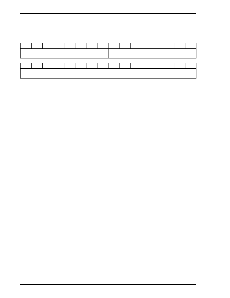
17-4
BitBLT Registers
&+,36
Æ
69000 Databook
Subject to Change Without Notice
Revision 1.3 8/31/98
BR02 Pattern/Source Expansion Foreground Color
Register
read/write at memory space offset 0x400008h
word or doubleword accessible
31-24
Reserved
These bits always return 0 when read.
23-0
Pattern/Source Expansion Foreground Color Bits 23-0
These 24 bits are used to specify the foreground color for the color expansion of either
monochrome pattern data only, or both monochrome pattern data and monochrome source
data (depending on the setting of bit 27 of BR03). When bit 27 of BR03 is set so that this
register is used in the color expansion of monochrome pattern data only, BR0A is used to
specify the foreground color for the color expansion of monochrome source data.
Whether bits 7-0, 15-0 or 23-0 of this register are used in the color expansion process
depends upon the color depth to which the BitBLT engine has been set.
31
30
29
28
27
26
25
24
23
22
21
20
19
18
17
16
Reserved
(0000:0000)
Pat/Src Expansion Foreground Color Bits 23-16
(xxxx:xxxx)
15
14
13
12
11
10
9
8
7
6
5
4
3
2
1
0
Pattern/Source Expansion Foreground Color Bits 15-0
(xxxx:xxxx:xxxx:xxxx)

BitBLT Registers
17-5
&+,36
Æ
69000 Databook
Subject to Change Without Notice
Revision 1.3 8/31/98
BR03 Monochrome Source Control Register
read/write at memory space offset 0x40000Ch
word or doubleword accessible
31-28
Reserved
These bits always return 0 when read.
27
Monochrome Source Expansion Color Register Select
0: This causes the background and foreground colors for the color expansion of
monochrome source data to be specified by BR01 and BR02, respectively.
1: This causes the background and foreground colors for the color expansion of
monochrome source data to be specified by BR09 and BR0A, respectively.
26-24
Monochrome Source Scanline Data Alignment
Note: These bits are used only when the source data is monochrome.
These 3 bits are used to configure the BitBLT engine for the byte alignment of each
scanline's worth of monochrome source data during a BitBLT operation, as each scanline's
worth of monochrome source data is received.
Refer to the section describing the BitBLT engine for further details concerning the
requirements for how monochrome source data must be organized.
31
30
29
28
27
26
25
24
23
22
21
20
19
18
17
16
Reserved
(0000)
Src
Exp
(x)
Mono Src Align
(xxx)
Reserved
(00)
Monochrome Source Data Initial Discard
(xx:xxxx)
15
14
13
12
11
10
9
8
7
6
5
4
3
2
1
0
Reserved
(00)
Monochrome Source Data Right Clipping
(xx:xxxx)
Reserved
(00)
Monochrome Source Data Left Clipping
(xx:xxxx)
Bit
26 25 24
Specified Monochrome Source Data Alignment
0 0 0
Reserved
0 0 1
Bit-Aligned
0 1 0
Byte-Aligned
0 1 1
Word-Aligned
1 0 0
Doubleword-Aligned
1 0 1
Quadword-Aligned
1 1 0
Reserved
1 1 1
Reserved

17-6
BitBLT Registers
&+,36
Æ
69000 Databook
Subject to Change Without Notice
Revision 1.3 8/31/98
23-22
Reserved
These bits always return 0 when read.
21-16
Monochrome Source Data Initial Discard
Note: These bits are used only when the source data is monochrome.
These 6 bits are used to specify how many bits (up to 63 bits) of monochrome source data
should be skipped over in the first quadword of source data in order to reach the first bit of
valid or desired monochrome source data. These bits are normally used to clip one or more
of the first scanline's worth of monochrome source data, (i.e. clipping monochrome source
data from the top).
15-14
Reserved
These bits always return 0 when read.
13-8
Monochrome Source Data Right Clipping
Note: These bits are used only when the source data is monochrome.
These 6 bits are used to specify how many bits (up to 63 bits) of monochrome source data
should be discarded from the end of each scanline's worth of valid or desired monochrome
source data. These bits are normally used to clip monochrome source data from the right.
7-6
Reserved
These bits always return 0 when read.
5-0
Source Data Left Clipping
Note: These bits are used only when the source data is monochrome.
These 6 bits are used to indicate how many bits (up to 63 bits) of monochrome source data
should be discarded from the beginning of each scanline's worth of valid or desired
monochrome source data. These bits are normally used to clip the monochrome source
data from the left.
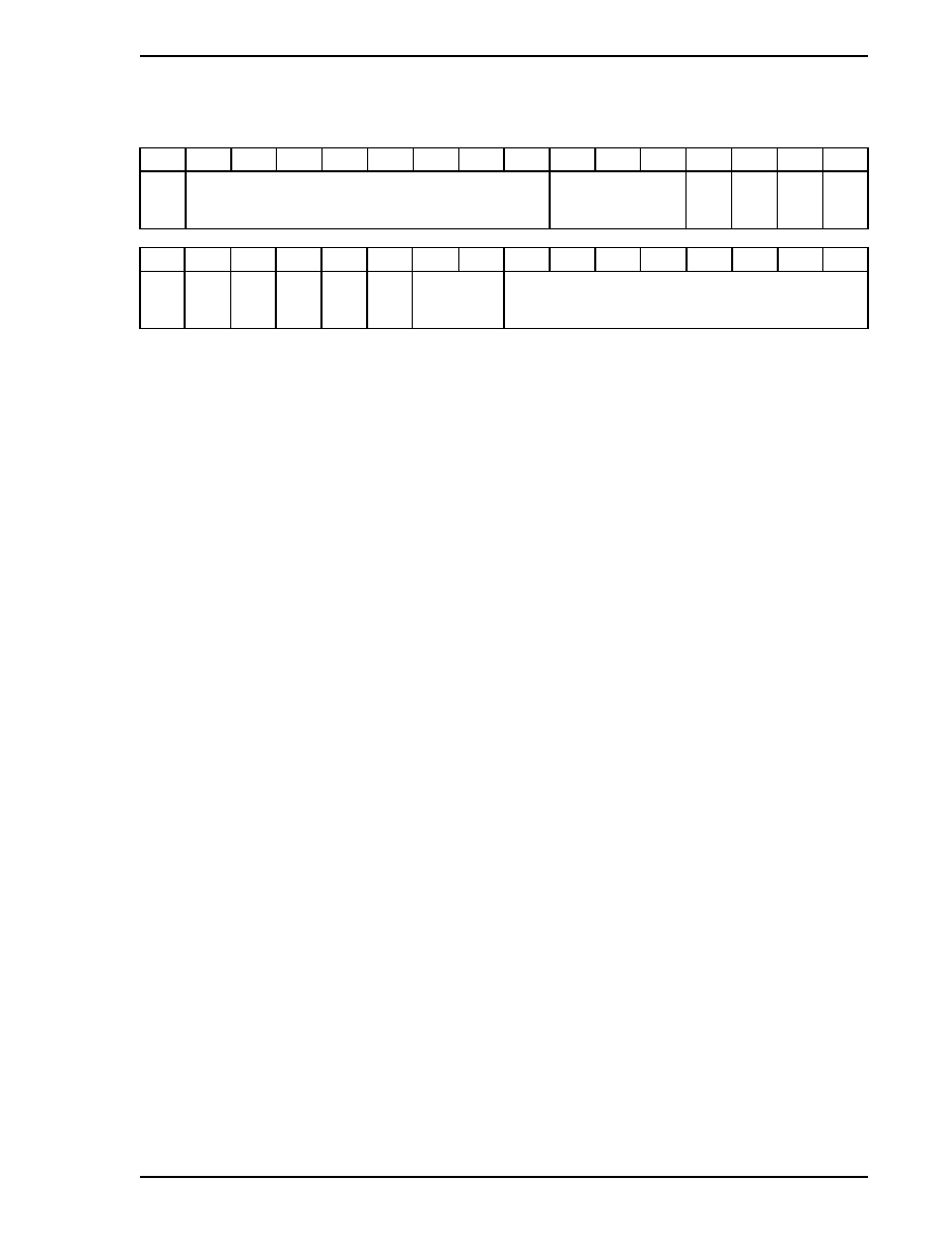
BitBLT Registers
17-7
&+,36
Æ
69000 Databook
Subject to Change Without Notice
Revision 1.3 8/31/98
BR04 BitBLT Control Register
read/write at memory space offset 0x400010h
word or doubleword accessible
31
BitBLT Engine Status
Note: This bit is read-only -- writes to this bit are ignored.
0: Indicates that the BitBLT engine is idle.
1: Indicates that the BitBLT engine is busy.
30-23
Reserved
These bits always return 0 when read.
22-20
Pattern Vertical Alignment
Specifies which scanline's worth (i.e., which 1 of the 8 horizontal rows) of the 8x8 pattern
data will appear in the first scanline's worth of the destination output data. Depending on
the location of the destination, the upper left corner of the upper left tile of the pattern data
is usually aligned with the upper left corner of the destination output data as the pattern data
is tiled into the destination. The BitBLT engine determines the horizontal alignment of the
leftmost tiles of pattern data relative to the destination using the lower order bits of the
destination address specified in BR07. However, the vertical alignment relative to the
destination must be specified using these 3 bits.
19
Solid Pattern Select
Note: This bit applies only when the pattern data is monochrome (determined by bit 18 of
this register).
0: Causes monochrome pattern data to actually be read and used as is normal, if indeed
monochrome pattern data is being used as an input to a BitBLT operation.
1: Causes the BitBLT engine to forgo the process of reading the pattern data. Instead, the
presumption is made that all of the bits of the pattern data are set to 0. The pattern operand
for all bit-wise operations is forced to the background color specified in BR01.
18
Pattern Color Depth
0: Specifies that the pattern data is in color and therefore can have a color depth of 8, 16,
or 24 bits per pixel.
1: Specifies that the pattern data is monochrome and therefore has a color depth of 1 bit
per pixel.
31
30
29
28
27
26
25
24
23
22
21
20
19
18
17
16
BB
Stat
(0)
Reserved
(000:0000:0)
Pattern Vertical
Alignment
(000)
Sol
Pat
(0)
Pat
Dep
(0)
Pat
Mask
(0)
Tran
Sel
(0)
15
14
13
12
11
10
9
8
7
6
5
4
3
2
1
0
Tran
Sel
(0)
Tran
Enl
(0)
Src
Mask
(0)
Src
Dep
(0)
Rsvd
(0)
Src
Sel
(0)
Starting
Point Select
(00)
Bit-Wise Operation
Select
(00h)

17-8
BitBLT Registers
&+,36
Æ
69000 Databook
Subject to Change Without Notice
Revision 1.3 8/31/98
17
Monochrome Pattern Write-Masking
Note: This bit applies only when the pattern data is monochrome (determined by bit 18 of
this register).
This bit enables a form of per-pixel write-masking in which monochrome pattern data is
used as a pixel mask that controls which pixels at the destination will be written to by the
BitBLT engine.
0: This disables the use of monochrome pattern data as a write mask, allowing normal
operation of the BitBLT engine with regard to the use of monochrome pattern data.
1: Wherever a bit in monochrome pattern data carries the value of 0 the byte(s) of the
corresponding pixel at the destination are NOT written, thereby preserving any data already
carried by those bytes.
16-15
Color Transparency Select
These 2 bits are used to select the type of color transparency to be performed.
When color transparency is enabled by setting bit 14 of this register to 1, the color value
carried within bits 23-0 of either BR01 or BR09 is used as a key color to mask the writing
of pixel data to the destination on a per-pixel basis. Before each pixel at the destination is
written, a comparison is made between this key color and another color, and whether or not
that given pixel at the destination will actually be written depends upon the result of that
comparison.
Whether BR01 or BR09 is used to supply the key color depends on the setting of bit 27 of
BR03 since the same register that is used to supply the key color for color transparency
also happens to be used to supply the background color for monochrome-to-color
expansion. Also, depending on the type of color transparency selected, the other color
value to which the key color is compared may be the color value resulting from the bit-wise
operation selected via bits 7-0 of this register.
Note: Color transparency can be used only when the BitBLT engine is set to a color depth
of 8 or 16 bits per pixel, but not 24 bits per pixel. If the BitBLT engine has been set to a
color depth of 24 bits per pixel, then bit 14 of this register should always remain set to 0 to
disable color transparency.
Bit
16 15
Form of Per-Pixel Color Comparison Selected
0 0
The color value carried by bits 23-0 of either BR01 or BR09 is compared to the color value
resulting from the bit-wise operation being performed for the current pixel. If these two
color values are NOT the same, then the byte(s) for the current pixel at the destination will
be written with the color value resulting from the bit-wise operation.
0 1
The color value carried by bits 23-0 of either BR01 or BR09 is compared to the color value
already specified in the byte(s) for the current pixel at the destination. If these two color
values are NOT the same, then the byte(s) for the current pixel at the destination will be
written with the color value resulting from the bit-wise operation.
1 0
The color value carried by bits 23-0 of either BR01 or BR09 is compared to the color value
resulting from the bit-wise operation being performed for the current pixel. If these two
color values ARE the same, then the byte(s) for the current pixel at the destination will be
written with the color value resulting from the bit-wise operation.
1 1
The color value carried by bits 23-0 of either BR01 or BR09 is compared to the color value
already specified in the byte(s) for the current pixel at the destination. If these two color
values ARE the same, then the byte(s) for the current pixel at the destination will be written
with the color value resulting from the bit-wise operation.

BitBLT Registers
17-9
&+,36
Æ
69000 Databook
Subject to Change Without Notice
Revision 1.3 8/31/98
14
Color Transparency Enable
These bit is used to enable or disable color transparency.
When color transparency is enabled, the color value carried within bits 23-0 of either BR01
or BR09 is used as a key color to mask the writing of pixel data to the destination on a per-
pixel basis. Before each pixel at the destination is written, a comparison is made between
this key color and another color, and whether or not that given pixel at the destination will
actually be written depends upon the result of that comparison.
Whether BR01 or BR09 is used to supply the key color depends on the setting of bit 27 of
BR03 since the same register that is used to supply the key color for color transparency
also happens to be used to supply the background color for monochrome-to-color
expansion. Also, depending on the type of color transparency selected via bits 16-15 of
this register, the other color value to which the key color is compared may be the color value
resulting from the bit-wise operation selected via bits 7-0 of this register.
0: Disables color transparency.
1: Enables color transparency.
Note: Color transparency can be used only when the BitBLT engine is set to a color depth
of 8 or 16 bits per pixel, but not 24 bits per pixel. If the BitBLT engine has been set to a
color depth of 24 bits per pixel, then this bit should always remain set to 0 to disable color
transparency.
13
Monochrome Source Write-Masking
Note: This bit applies only when the source data is monochrome (determined by bit 12 of
this register).
This bit enables a form of per-pixel write-masking in which monochrome source data is
used as a pixel mask that controls which pixels at the destination will be written to by the
BitBLT engine.
0: This disables the use of monochrome source data as a write mask, allowing normal
operation of the BitBLT engine with regard to the use of monochrome source data.
1: Wherever a bit in monochrome source data carries the value of 0, the byte(s) of the
corresponding pixel at the destination are NOT written, thereby preserving any data already
carried by those bytes.
12
Source Color Depth
0: Specifies that the source data is in color, and therefore, can have a color depth of 8, 16,
or 24 bits per pixel.
1: Specifies that the source data is monochrome, and therefore, has a color depth of 1 bit
per pixel. This setting should be used only if bit 8 of this register is set to 0.
Note: This bit must be set to 0 whenever a bit-wise operation is selected (using bits 7-0 of
this register) that does not use source data.
11
Reserved (Writable)
This bit should always be written with the value of 0.
10
Source Select
0: Configures the BitBLT engine to read the source data from the frame buffer at the
location specified in BR06.
1: Configures the BitBLT engine to accept the source data from the host CPU via the
BitBLT data port. The host CPU provides the source data by performing a series of
memory write operations to the BitBLT data port.

17-10
BitBLT Registers
&+,36
Æ
69000 Databook
Subject to Change Without Notice
Revision 1.3 8/31/98
9-8
Starting Point Select
These two bits are used to select which of the four corners to use as the starting point in
reading and writing graphics data in a BitBLT operation. Normally, the upper left corner is
used. However, situations involving an overlap of source and destination locations (this
usually occurs when the source and destination locations are both on-screen) often require
the use of a different corner as a starting point. It should be remembered that the
addresses specified for each piece of graphics data used in a BitBLT operation must point
to the byte(s) corresponding to whichever pixel is at the selected starting point. If the
starting point is changed, then these addresses must also be changed. See the chapter on
the BitBLT engine for more information.
7-0
Bit-Wise Operation Select
These 8 bits are meant to be programmed with an 8-bit code that selects which one of 256
possible bit-wise operations is to be performed by the BitBLT engine during a BitBLT
operation. These 256 possible bit-wise operations and their corresponding 8-bit codes are
designed to be compatible with the manner in which raster operations are specified in the
standard BitBLT parameter block normally used in the Microsoft Windows environment,
without translation. See the section on the BitBLT engine for more information.
Note: Bit 12 of this register must be set to 0 whenever a bit-wise operation is selected that
does not use source data.
Bit
9 8
Corner Selected as the Starting Point
0 0
Upper Left Corner -- This is the default after reset.
0 1
Upper Right Corner
1 0
Lower Left Corner
1 1
Lower Right Corner

BitBLT Registers
17-11
&+,36
Æ
69000 Databook
Subject to Change Without Notice
Revision 1.3 8/31/98
BR05 Pattern Address Register
read/write at memory space offset 0x400014h
word or doubleword accessible
31-22
Reserved (Writable)
These bits should always be written with the value of 0.
21-3
Pattern Address
These bits specify the starting address of the pattern data within the frame buffer as an
offset from the beginning of the frame buffer to where the first byte of pattern data is located.
The pattern data is always an 8x8 array of pixels that is always stored in frame buffer
memory as a single contiguous block of bytes. The pattern data must be located on a
boundary within the frame buffer that is equivalent to its size, and its size depends on the
pattern data's color depth. The color depth may be 1 bit per pixel if the pattern data is
monochrome or it may be 8, 16, or 24 bits per pixel if the pattern data is in color (the color
depth of a color pattern must match the color depth to which the BitBLT engine has been
set). Monochrome patterns require 8 bytes, and so the pattern data must start on a
quadword boundary. Color patterns of 8, 16, and 24 bits per pixel color depth must start
on 64-byte, 128-byte, and 256-byte boundaries, respectively.
Note: In the case of 24 bits per pixel, each row of 8 pixels of pattern data takes up 32
consecutive bytes, not 24. The pattern data is formatted so that for each row there is a
block of 8 sets of 3 bytes (each set corresponding to one of the 8 pixels), followed by a block
of the 8 extra bytes. When the BitBLT engine reads 24 bit-per-pixel pattern data, it will read
only the first 24 bytes of each row of pattern data, picking up only the 8 sets of 3 bytes for
the 8 pixels in that row, and entirely ignoring the remaining 8 bytes.
2-0
Reserved
These bits always return 0 when read.
31
30
29
28
27
26
25
24
23
22
21
20
19
18
17
16
Reserved
(0000:0000:00)
Pattern Address Bits 21-16
(xx:xxxx)
15
14
13
12
11
10
9
8
7
6
5
4
3
2
1
0
Pattern Address Bits 15-3
(xxxx:xxxx:xxxx:x)
Reserved
(000)

17-12
BitBLT Registers
&+,36
Æ
69000 Databook
Subject to Change Without Notice
Revision 1.3 8/31/98
BR06 Source Address Register
read/write at memory space offset 0x400018h
word or doubleword accessible
Important: This register should never be read while the BitBLT engine is busy.
31-22
Reserved (Writable)
These bits should always be written with the value of 0.
21-0
Source Address
When the source data is located within the frame buffer, these bits are used to specify the
starting address of the source data within the frame buffer as an offset from the beginning
of the frame buffer to where the first byte of source data is located.
When the source data is provided by the host CPU through the BitBLT data port, and that
source data is in color, only bits 2-0 are used and the upper bits are ignored. These lower
3 bits are used to indicate the position of the first valid byte within the first quadword of the
source data.
When the source data is provided by the host CPU through the BitBLT data port, and that
source data is monochrome, the BitBLT engine ignores this register entirely.
31
30
29
28
27
26
25
24
23
22
21
20
19
18
17
16
Reserved
(0000:0000:00)
Source Address Bits 21-16
(xx:xxxx)
15
14
13
12
11
10
9
8
7
6
5
4
3
2
1
0
Source Address Bits 15-0
(xxxx:xxxx:xxxx:xxxx)

BitBLT Registers
17-13
&+,36
Æ
69000 Databook
Subject to Change Without Notice
Revision 1.3 8/31/98
BR07 Destination Address Register
read/write at memory space offset 0x40001Ch
word or doubleword accessible
Important: This register should never be read while the BitBLT engine is busy.
31-22
Reserved (Writable)
These bits should always be written with the value of 0.
21-0
Destination Address
These bits are used to specify the starting address of the destination location within the
frame buffer as an offset from the beginning of the frame buffer to where the first byte of
the destination location.
The destination location is the location from which destination input data (if used) will be
read, and it is where the destination output data will be written.
31
30
29
28
27
26
25
24
23
22
21
20
19
18
17
16
Reserved
(0000:0000:00)
Destination Address Bits 21-16
(xx:xxxx)
15
14
13
12
11
10
9
8
7
6
5
4
3
2
1
0
Destination Address Bits 15-0
(xxxx:xxxx:xxxx:xxxx)

17-14
BitBLT Registers
&+,36
Æ
69000 Databook
Subject to Change Without Notice
Revision 1.3 8/31/98
BR08 Destination Width & Height Register
read/write at memory space offset 0x400020h
word or doubleword accessible
Important: This register should never be read while the BitBLT engine is busy.
31-29
Reserved
These bits always return 0 when read.
28-16
Destination Scanline Height
These 13 bits specify the height of the destination input and output data in terms of the
number of scanlines.
15-13
Reserved
These bits always return 0 when read.
12-0
Destination Byte Width
These 13 bits specify the width of the destination input and output data in terms of the
number of bytes per scanline's worth. The number of pixels per scanline into which this
value translates depends upon the color depth to which the BitBLT engine has been set.
31
30
29
28
27
26
25
24
23
22
21
20
19
18
17
16
Reserved
(000)
Destination Scanline Height
(0:0000:0000:0000)
15
14
13
12
11
10
9
8
7
6
5
4
3
2
1
0
Reserved
(000)
Destination Byte Width
(0:0000:0000:0000)

BitBLT Registers
17-15
&+,36
Æ
69000 Databook
Subject to Change Without Notice
Revision 1.3 8/31/98
BR09 Source Expansion Background Color &
Transparency Key Register
read/write at memory space offset 0x400024h
word or doubleword accessible
31-24
Reserved
These bits always return 0 when read.
23-0
Source Expansion Background Color & Transparency Key Bits 23-0
These 24 bits are optionally used to specify the background color for the color expansion
of monochrome source data (depending on the setting of bit 27 of BR03). When bit 27 of
BR03 is set so that this register is used in the color expansion of monochrome source data,
BR01 is used to specify the background color for the color expansion of monochrome
pattern data.
These 24 bits are also optionally used to specify the key color for whichever form of color
transparency is selected via bits 16-15 of BR04 (depending on the setting of bit 27 of
BR03).
Whether bits 7-0, 15-0 or 23-0 of this register are used in both the color expansion and color
transparency processes depends upon the color depth to which the BitBLT engine has
been set.
31
30
29
28
27
26
25
24
23
22
21
20
19
18
17
16
Reserved
(0000:0000)
Src Expansion Background Color & Transparency Key
Bits 23-16
(xxxx:xxxx)
15
14
13
12
11
10
9
8
7
6
5
4
3
2
1
0
Source Expansion Background Color & Transparency Key Bits 15-0
(xxxx:xxxx:xxxx:xxxx)

17-16
BitBLT Registers
&+,36
Æ
69000 Databook
Subject to Change Without Notice
Revision 1.3 8/31/98
BR0A Source Expansion Foreground Color Register
read/write at memory space offset 0x400028h
word or doubleword accessible
31-24
Reserved
These bits always return 0 when read.
23-0
Pattern/Source Expansion Foreground Color Bits 23-0
These 24 bits are optionally used to specify the foreground color for the color expansion of
monochrome source data (depending on the setting of bit 27 of BR03). When bit 27 of
BR03 is set so that this register is used in the color expansion of monochrome source data,
BR02 is used to specify the foreground color for the color expansion of monochrome
pattern data.
Whether bits 7-0, 15-0 or 23-0 of this register are used in the color expansion process
depends upon the color depth to which the BitBLT engine has been set.
31
30
29
28
27
26
25
24
23
22
21
20
19
18
17
16
Reserved
(0000:0000)
Source Expansion Foreground Color Bits 23-16
(xxxx:xxxx)
15
14
13
12
11
10
9
8
7
6
5
4
3
2
1
0
Source Expansion Foreground Color Bits 15-0
(xxxx:xxxx:xxxx:xxxx)

Memory-Mapped Wide Extension Registers
18-1
&+,36
Æ
69000 Databook
Subject to Change Without Notice
Revision 1.3 8/31/98
Chapter 18
Memory-Mapped Wide Extension Registers
The video decoder registers are 32-bit memory-mapped registers that exist in the upper memory space that
the 69000 occupies on the host bus. Refer to chapter on address maps for more information. These
registers exist at an offset of 0x400100h from the base address of the memory space.
Name
Function
Access
Offset
ER00
Central Interrupt Control Register
read/write
0x400600
ER01
Central Interrupt Status Register
read/write
0x400604
ER03
Miscellaneous Function Register
read/write
0x40060C
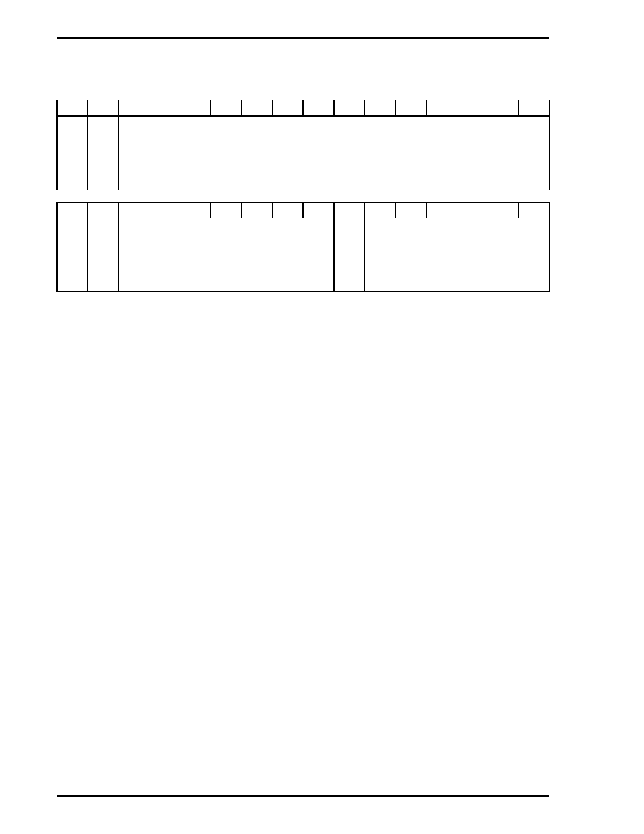
18-2
Memory-Mapped Wide Extension Registers
&+,36
Æ
69000 Databook
Subject to Change Without Notice
Revision 1.3 8/31/98
ER00 Central Interrupt Control Register
read/write at memory space offset 0x400100h
word or doubleword accessible
31
BitBLT Engine Idle Interrupt Output Enable
0: No hardware interrupt is output to the host when the BitBLT engine becomes idle after
performing a BitBLT operation.
1: Causes a hardware interrupt to be output to the host when the BitBLT engine becomes
idle after performing a BitBLT operation.
30
Reserved
This bit always returns a value of 0 when read.
29-15
Reserved
These bits always return the value of 0 when read.
14
Display Vertical Blanking Period Interrupt Output Enable
0: No hardware interrupt is output to the host when the last pixel of the last scan line within
the active display area is drawn on pipeline A.
1: Causes a hardware interrupt to be output to the host when the last pixel of the last scan
line within the active display area is drawn on pipeline A.
13-7
Reserved
These bits always return the value of 0 when read.
6
Video Capture Vertical Sync Interrupt Output Enable
0: No hardware interrupt is output to the host at the start of each vertical sync pulse from
the acquisition data source.
1: Causes a hardware interrupt to be output to the host at the start of each vertical sync
pulse from the acquisition data source.
5-0
Reserved
These bits always return the value of 0 when read.
31
30
29
28
27
26
25
24
23
22
21
20
19
18
17
16
BBLT
Idle
Int
Output
En
(0)
Rsrvd
(0)
Reserved
(00:0000:0000:0000)
15
14
13
12
11
10
9
8
7
6
5
4
3
2
1
0
Rsvd
(0)
Dsply
VBlnk
Int
Output
En
(0)
Reserved
(00:0000:0)
V Cap
VSync
Int
Output
En
(0)
Reserved
(00:0000)

Memory-Mapped Wide Extension Registers
18-3
&+,36
Æ
69000 Databook
Subject to Change Without Notice
Revision 1.3 8/31/98
ER01 Central Interrupt Status/Acknowledge Register
read/write at memory space offset 0x400104h
word or doubleword accessible
31
BitBLT Engine Idle Interrupt Pending
0: Since this bit was last cleared, no interrupt has been sourced as a result of the BitBLT
engine becoming idle after performing a BitBLT operation.
1: An interrupt was sourced as a result of the BitBLT engine becoming idle after performing
a BitBLT operation. Writing the value of 1 to this bit will clear it to 0 (writing the value of 0
to this bit has no effect and will be ignored).
30
Reserved
These bits always return the value of 0 when read.
29-15
Reserved
These bits always return the value of 0 when read.
14
Display Vertical Blanking Period Interrupt Pending
0: Since this bit was last cleared, no interrupt has been sourced as a result of the drawing
of the last scan line within the active display area on pipeline A.
1: An interrupt was sourced as a result of the drawing of the last scan line within the active
display area on pipeline A. Writing the value of 1 to this bit will clear it to 0 (writing the value
of 0 to this bit has no effect and will be ignored).
13-7
Reserved
These bits always return the value of 0 when read.
6
Video Capture Vertical Sync Interrupt Pending
0: Since this bit was last cleared, no interrupt has been sourced as a result of the start of
a vertical sync pulse from the acquisition data source.
1: An interrupt was sourced as a result of the start of a vertical sync pulse from the
acquisition data source. Writing the value of 1 to this bit will clear it to 0 (writing the value
of 0 to this bit has no effect and will be ignored).
5-0
Reserved
These bits always return the value of 0 when read.
31
30
29
28
27
26
25
24
23
22
21
20
19
18
17
16
BBLT
Idle
(0)
Reserved
(00:0000:0000:0000)
15
14
13
12
11
10
9
8
7
6
5
4
3
2
1
0
Rsvd
(0)
Pipe A
V Blnk
(0)
Reserved
(00:0000:0)
V Cap
VSync
(0)
Reserved
(00:0000)

18-4
Memory-Mapped Wide Extension Registers
&+,36
Æ
69000 Databook
Subject to Change Without Notice
Revision 1.3 8/31/98
ER03 Miscellaneous Function Register
read/write at memory space offset 0x40010Ch
word or doubleword accessible
32-15
Reserved
This bit always returns the value of 0 when read.
14
Display Vertical Blanking Period Interrupt Source Polarity
0: No inversion.
1: Inversion.
13-7
Reserved
These bits always return the value of 0 when read.
6
Video Capture Vertical Sync Interrupt Source Polarity
0: No inversion.
1: Inversion.
5-0
Reserved
These bits always return the value of 0 when read.
31
30
29
28
27
26
25
24
23
22
21
20
19
18
17
16
Reserved
(0000:0000:0000:0000)
15
14
13
12
11
10
9
8
7
6
5
4
3
2
1
0
Rsvd
(0)
Dsply
Vert
Blnk
Pol
(0)
Reserved
(00:0000:0)
VCap
VSync
Int
Pol
(0)
Reserved
(00:0000)

A-1
&+,36
Æ
69000 Databook
Subject to Change Without Notice
Revision 1.3 8/31/98
Appendix A
DISPLAY MODES
This chapter lists tables for configuring the 69000 for various CRT monitor and flat panel graphics and text
display modes. The parameters detailed in the tables of this chapter define standard capabilities of the
69000 when it is used with the Chips VGA BIOS. Consult with the appropriate BIOS vendor for information
about display modes and parameters that are supported by BIOSs that are not from Chips.
The following symbols and abbreviations are used for display modes in the following sections:
≠
Indicates CGA display mode(Table A-1 only.)
*
EGA display mode. (Table A-1 only.)
+
VGA display mode. (Table A-1 only.)
DSTN
Dual-scan STN flat panel
I
Interlaced
L
Linear mapped
P
Page mapped

A-2
&+,36
Æ
69000 Databook
Subject to Change Without Notice
Revision 1.3 8/31/98
CRT-Only Display Modes
This section lists tables for standard VGA and Chips Extended VGA CRT-only display modes.
Standard VGA CRT-Only Display Modes
The 69000 VGA BIOS supports all standard VGA CRT-only display modes, listed below.
Table A-1: Standard VGA CRT-Only Display Modes
Standard
VGA
Display
Mode No.
(hex)
VESA
Display
Mode
Number
Color
Resolution
(bpp/
# colors)
Characters
X
Rows
Character
Cell
(pixels)
Resolution
(pixels)
Type of
Display
Mode
Horizontal
Frequency
(kHz)
Vertical
Frequency
(Hz)
00, 01
≠
16/256K
40
◊
25
8
◊
8
320
◊
200
Text
31.5
70
00*, 01*
≠
16/256K
40
◊
25
8
◊
14
320
◊
350
Text
31.5
70
00+, 01+
≠
16/256K
40
◊
25
9
◊
16
360
◊
400
Text
31.5
70
02, 03
≠
16/256K
80
◊
25
8
◊
8
640
◊
200
Text
31.5
70
02*, 03*
≠
16/256K
80
◊
25
8
◊
14
640
◊
350
Text
31.5
70
02+, 03+
≠
16/256K
80
◊
25
9
◊
16
720
◊
400
Text
31.5
70
04, 05
≠
4/256K
40
◊
25
8
◊
8
320
◊
200
Graphics
31.5
70
06
≠
2/256K
80
◊
25
8
◊
8
640
◊
200
Graphics
31.5
70
07*
≠
Mono-
chrome
80
◊
25
9
◊
14
720
◊
350
Text
31.5
70
07+
≠
Mono-
chrome
80
◊
25
9
◊
16
720
◊
400
Text
31.5
70
0D
≠
16/256K
40
◊
25
8
◊
8
320
◊
200
Graphics
31.5
70
0E
≠
16/256K
80
◊
25
8
◊
8
640
◊
200
Graphics
31.5
70
0F
≠
Mono
80
◊
25
8
◊
14
640
◊
350
Graphics
31.5
70
10
≠
16/256K
80
◊
25
8
◊
14
640
◊
350
Graphics
31.5
70
11
≠
2/256K
80
◊
30
8
◊
16
640
◊
480
Graphics
31.5
60
12
≠
16/256K
80
◊
30
8
◊
16
640
◊
480
Graphics
31.5
60
13
≠
256/256K
40
◊
25
8
◊
8
320
◊
200
Graphics
31.5
70

A-3
&+,36
Æ
69000 Databook
Subject to Change Without Notice
Revision 1.3 8/31/98
Chips Extended VGA CRT-Only Display Modes
Table A-2 shows the extended VGA and VESA display modes that the 69000 VGA BIOS supports.
Within the table:
∑
The `Minimum MCLK' column gives the recommended memory clock frequency at which
the 69000 can run without adverse effects to functionality. Better benchmarks can be
achieved with an MCLK frequency higher than the frequency specified.
∑
Some of the display modes are not supported by all CRT monitors.
Table A-2: Extended VGA CRT-Only Display Modes
Extended
VGA
Display
Mode No.
(hex)
VESA
Display
Mode No.
(hex)
Color
Depth
(bits per
pixel)
Memory
Organization
Resolution
(pixels)
Horizontal
Freq.
(kHz)
Vertical
Freq.
(Hz)
VCLK
(MHz)
Mini-
mum
MCLK
(MHz)
14h
≠
8
Packed Pixel
320
◊
200
31.5
70
12.587
50
15h
16
31.5
70
12.587
50
16h
24
31.5
70
12.587
50
17h
≠
8
Packed Pixel
320
◊
240
31.5
60
12.587
50
18h
16
31.5
60
12.587
50
19h
24
31.5
60
12.587
50
1Ah
≠
8
Packed Pixel
400
◊
300
37.5
60
20
50
1Bh
16
37.5
60
20
50
1Ch
24
37.5
60
20
50
1Dh
≠
Packed Pixel
512
◊
384
48.4
60
32.5
50
1Eh
≠
256/256K
48.4
60
32.5
50
1Fh
≠
48.4
60
32.5
50
31h
100h
8
Packed Pixel
640 x 400
31.5
70
25.175
50
62h
≠
16
31.5
70
25.175
50
63h
≠
24
31.5
70
25.175
50
20h
120h
4
Packed Pixel
640 x 480
31.5
60
25.175
50
37.5
75
31.5
50
43.3
85
36
50
22h
122h
4
Packed Pixel
800 x 600
35.5
56
36
50
46.9
60
40
50
46.9
75
49.5
50
53.7
85
56.25
50
6Ah
102
4
Planar
800 x 600
31.5
56
36
50
37.9
60
40
50
46.9
75
49.5
50
53.7
85
56.25
50

A-4
&+,36
Æ
69000 Databook
Subject to Change Without Notice
Revision 1.3 8/31/98
Extended
VGA
Display
Mode No.
(hex)
VESA
Display
Mode No.
(hex)
Color
Depth
(bits per
pixel)
Memory Organiza-
tion
Resolution
(pixels)
Horizontal
Freq.
(kHz)
Vertical
Freq.
(Hz)
VCLK
(MHz)
Mini-
mum
MCLK
(MHz)
24h
102h
4
Packed Pixel
800 x 600
31.5
60
25
50
37.9
72
31.5
50
37.5
75
31.5
50
43.269
85
36
50
64h
104h
4
Planar
1024
◊
768
35.5
43(I)
44.9
50
48.4
60
65
50
60
75
78.75
50
68.7
85
94.5
50
28h
128h
4
Packed Pixel
1280
◊
1024
47
43(I)
78.75
50
64
60
108
50
79.98
75
135
50
68h
106h
4
Planar
1280
◊
1024
47
43(I)
78.75
50
64
60
108
50
79.98
75
135
50
30h(L)
70h(P)
101h
8
Packed Pixel
640 x 480
31.5
60
25.175
50
37.5
75
31.5
50
43.3
85
36
50
31h(L)
71h(P)
100h
8
Packed Pixel
640 x 400
31.5
70
25.175
50
32h(L)
72h(P)
103h
8
Packed Pixel
800 x 600
35.1
56
36
50
37.9
60
40
50
46.9
75
49.5
58
53.7
85
56.25
68
34h(L)
74h(P)
105h
8
Packed Pixel
1024
◊
768
35.5
43(I)
44.9
50
48.4
60
65
60
60
75
78.75
80
68.7
85
94.5
80
36h
≠
8
Packed Pixel
Generic
≠
≠
≠
≠
38h(L)
78h(P)
107h
8
Packed Pixel
1280
◊
1024
47
43(I)
78.75
50
64
60
108
50
79.98
75
135
50

A-5
&+,36
Æ
69000 Databook
Subject to Change Without Notice
Revision 1.3 8/31/98
Extended
VGA
Display
Mode No.
(hex)
VESA
Display
Mode No.
(hex)
Color
Depth
(bits per
pixel)
Memory Organiza-
tion
Resolution
(pixels)
Horizontal
Freq.
(kHz)
Vertical
Freq.
(Hz)
VCLK
(MHz)
Mini-
mum
MCLK
(MHz)
41h
111h
16
Packed Pixel
640 x 480
31.5
60
25.175
50
37.5
75
31.5
50
43.3
85
36
50
43h
114h
16
Packed Pixel
800 x 600
35.1
56
36
50
37.9
60
40
50
46.9
75
49.5
60
53.7
85
56.25
70
45h
117h
16
Packed Pixel
1024 x 768
35.5
43(I)
44.9
50
48.4
60
65
50
60
75
78.75
50
68.7
85
94.5
50
47h
≠
16
Packed Pixel
Generic
≠
≠
≠
≠
50h
112h
24
Packed Pixel
640 x 480
31.5
60
25.175
50
37.5
75
31.5
50
43.3
85
36
50
52h
115h
24
Packed Pixel
800 x 600
35.5
56
36
50
37.9
60
40
50
46.9
75
49.5
50
53.7
85
56.25
50
56h
≠
24
Packed Pixel
Generic
≠
≠
≠
≠

A-6
&+,36
Æ
69000 Databook
Subject to Change Without Notice
Revision 1.3 8/31/98
Display Modes
The 69000 VGA BIOS supports flat panel-only and simultaneous operations with the standard VGA display
modes listed in here and elsewhere. In addition, the 69000 VGA BIOS supports flat panel-only and
simultaneous operations with the extended display modes listed in this section.
Flat Panel-Only and Simultaneous 640 x 480 (VGA) Display
Modes
For 640 x 480 flat panels, the Chips VGA BIOS supports flat panel-only and simultaneous operations with
the standard VGA display modes listed in Table A-1 and the extended VGA display modes in Table A-3.
∑
Within the table, the `Minimum MCLK' column gives the recommended memory clock
frequency at which the 69000 can run without adverse effects to functionality. Better
benchmarks can be achieved with an MCLK frequency higher than the frequency specified.
∑
DSTN flat panels require display memory for frame accelerator functionality.
∑
For simultaneous operation, both the flat panel and the CRT monitor must be configured at
a minimum to support the resolution of a given display mode.
Table A-3: Flat Panel-Only and Simultaneous 640 x 480 (VGA) Display Modes
Extended VGA Display
Mode Number (hex)
VESA Display
Mode Number
(hex)
Color Depth
(bits per pixel)
Resolution
(pixels)
Type of Flat
Panel
VCLK
(MHz)
Minimum
MCLK(MHz)
20h
120h
4
640
◊
400
DSTN/TFT
25
50
30h
101h
8
640
◊
480
DSTN/TFT
25
50
41h
111h
16
640
◊
480
DSTN/TFT
25
50
50h
112h
24
640
◊
480
DSTN/TFT
25
50

A-7
&+,36
Æ
69000 Databook
Subject to Change Without Notice
Revision 1.3 8/31/98
Flat Panel-Only and Simultaneous 800 x 600 (SVGA)
Display Modes
For 800 x 600 flat panels, the Chips VGA BIOS supports flat panel-only and simultaneous operations with
the standard VGA display modes listed in Table A-1 and the extended VGA display modes in Table A-4.
∑
Within the table, the `Minimum MCLK' column gives the recommended memory clock
frequency at which the 69000 can run without adverse effects to functionality. Better
benchmarks can be achieved with an MCLK frequency higher than the frequency specified.
∑
DSTN flat panels require display memory for frame accelerator functionality.
∑
For simultaneous operation, both the flat panel and the CRT monitor must be configured at
a minimum to support the resolution of a given display mode.
Table A-4: Flat Panel-Only and Simultaneous Display Modes for 800 x 600 Flat Panels.
a- planar mode
Extended VGA
Display Mode No.
(hex)
VESA
Display Mode
No. (hex)
Color Depth
(bits per pixel)
Resolution
(pixels)
Type of Flat Panel
VCLK
(MHz)
Minimum
MCLK
(MHz)
22h
122h
4
800
◊
600
DSTN
40
50
TFT
40
50
6Ah
a
102h
4
800
◊
600
DSTN
40
50
TFT
40
50
32h
103h
8
800
◊
600
DSTN
40
50
TFT
40
50
43h
114h
16
800
◊
600
DSTN
40
50
TFT
40
50
52h
115h
24
800
◊
600
DSTN
40
50
TFT
40
50
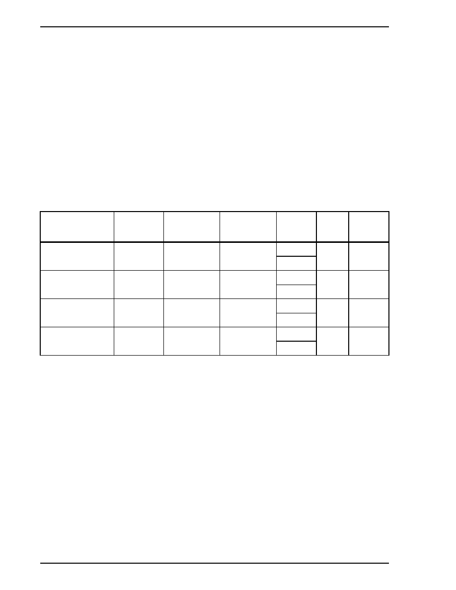
A-8
&+,36
Æ
69000 Databook
Subject to Change Without Notice
Revision 1.3 8/31/98
Flat Panel-Only and Simultaneous 1024 x 768 Display
Modes
For 1024 x 768 flat panels, the Chips VGA BIOS supports flat panel-only and simultaneous operations with
the standard VGA display modes listed in Table A-1 and the extended VGA display modes in Table A-5.
∑
Within the table, the `Minimum MCLK' column gives the recommended memory clock
frequency at which the 69000 can run without adverse effects to functionality. Better
benchmarks can be achieved with an MCLK frequency higher than the frequency specified.
∑
DSTN flat panels require display memory for frame accelerator functionality.
∑
For simultaneous operation, both the flat panel and the CRT monitor must be configured at
a minimum to support the resolution of a given display mode.
Table A-5: Flat Panel-Only and Simultaneous Display Modes for 1024 x 768 Flat Panels
a- planar mode
Extended VGA Display
Mode Number
(hex)
VESA Display
Mode Number
(hex)
Color Depth (bits
per pixel)
Resolution
(pixels)
Type of Flat
Panel
VCLK
(MHz)
Minimum
MCLK
(MHz)
24h
124h
4
1024
◊
768
DSTN
65
58
TFT
64h
a
104h
4
1024
◊
768
DSTN
65
58
TFT
34h
105h
8
1024
◊
768
DSTN
65
58
TFT
45h
117h
16
1024
◊
768
DSTN
65
58
TFT

A-9
&+,36
Æ
69000 Databook
Subject to Change Without Notice
Revision 1.3 8/31/98
Flat Panel-Only and Simultaneous 1280 x 1024 Display
Modes
For 1280 x 1024 flat panels, the Chips VGA BIOS supports flat panel-only and simultaneous operations with
the standard VGA display modes listed in Table A-1 and the extended VGA display modes in Table A-6.
∑
Within the table, the `Minimum MCLK' column gives the recommended memory clock
frequency at which the 69000 can run without adverse effects to functionality. Better
benchmarks can be achieved with an MCLK frequency higher than the frequency specified.
∑
DSTN flat panels require display memory for frame accelerator functionality.
∑
For simultaneous operation, both the flat panel and the CRT monitor must be configured at
a minimum to support the resolution of a given display mode.
Table A-6: Flat Panel-Only and Simultaneous Display Modes for 1280 x 1024 Flat Panels
a- planar mode
Extended VGA Display
Mode Number
(hex)
VESA Display
Mode Number
(hex)
Color Depth (bits
per pixel)
Resolution
(pixels)
Type of Flat
Panel
VCLK
(MHz)
Minimum
MCLK
(MHz)
28h
128h
4
1280 x 1024
DSTN
108
50
TFT
68h
a
106h
4
1280 x 1024
DSTN
108
50
TFT
38h
107h
8
1280 x 1024
TFT
108
50

A-10
&+,36
Æ
69000 Databook
Subject to Change Without Notice
Revision 1.3 8/31/98

Clock Generation
B-1
&+,36
Æ
69000 Databook
Subject to Change Without Notice
Revision 1.3 8/31/98
Appendix B
Clock Generation
Clock Synthesizer
The graphics controller contains two complete phase-locked loops (PLLs) to synthesize the internal Dot
Clock (DCLK) and Memory Clock (MCLK) from an externally supplied reference frequency. Each of the two
clock synthesizer phase lock loops may be programmed to output frequencies ranging between 3MHz and
the maximum specified operating frequency for that clock in increments not exceeding 0.5%. An external
crystal-controlled oscillator (TTL) generates the reference frequency of 14.31818 MHz that is driven into the
graphics controller on pin C3. The graphics controller can not generate the 14.31818 MHz reference
frequency using only an external crystal.
Dot Clock (DCLK)
The dot clock is used as the basis for all display timing. The horizontal and vertical sync frequencies are
derived by dividing down the dot clock.
In borrowing from VGA parlance, there are said to be three dot clocks: DCLK0, DCLK1 and DCLK2. In
truth, there is actually only a single PLL, but it can be configured with divisor values from any one of three
sets of registers within the XRC0-XRCF group of registers, and these three groups of registers are referred
to as if they were DCLK0, DCLK1 and DCLK2. Bits 3 and 2 of the Miscellaneous Output Register (MSR)
are used to select which one of these 3 sets of registers will be used to supply the divisor values that the
PLL will use in creating the dot clock at any given time.
During reset, the first two sets of these registers (DCLK0 and DCLK1) default to values that specify the two
standard VGA dot clocks of 25.175MHz and 28.322MHz, and normally the values in these first two sets of
registers are not changed. The third set of registers (DCLK2) is used for all modes that are not of the VGA
standard, i.e., the extended modes.
Memory Clock (MCLK)
The memory clock is used as the basis for all memory timing. It is normally set once following hardware
reset, and is not normally modified again.

B-2
Clock Generation
&+,36
Æ
69000 Databook
Subject to Change Without Notice
Revision 1.3 8/31/98
PLL Parameters
Each phase-locked loop consists of the elements shown in the figure below. The reference input frequency
(14.31818MHz) is divided by N, a 8-bit programmable value. The output of the VCO is divided by 1 (or 4
via the VCO Loop Divider: VLD) and then further divided by M, another 8-bit programmable value. The
phase detector compares the N and M results and adjusts the VCO frequency as needed to achieve
frequency equality.
When the loop has stabilized, the VCO frequency (F
VCO
) is related to the reference as follows:
If VLD=1:
F
VCO
/M = F
REF
/ N
or
If VLD=4:
F
VCO
/4M = F
REF
/ N.
(DCLK only)
For VLD =1, the F
VCO
can be written as:
F
VCO
= (F
REF
*M /N)
The VCO output can be further divided by 1, 2, 4, 8, 16, or 32 (which is called Post Divisor: PD) to produce
the final DCLK or MCLK used for video or memory timing.
Therefore the output frequency is:
F
OUT
= (F
VCO
)/PD
By "fine tuning" the M/N ratio in each PLL, extremely small adjustments in the exact DCLK and MCLK
frequencies can be achieved. The VCO itself is designed to operate in the range of 100MHz to 220 MHz.
Figure B-1: PLL Elements
M counter = Program value M'+2
F
VCO
: VCO frequency (before post divisor)
N counter = Program value N'+2
F
OUT
: Output frequency: (desired frequency)
C LK
F
O UT
P ost D ivisor
(PD )
˜1, 2, 4,
8, 16, 32
V C O Loop
D ivide (V LD )
(˜4, ˜1)
˜M
P hase
D etect
C harge Pum p
& Filter
V C O
˜
N
F
VC O
R E F C L K
14 .3 M H z
(D C LK o nly)

Clock Generation
B-3
&+,36
Æ
69000 Databook
Subject to Change Without Notice
Revision 1.3 8/31/98
Programming the Clock Synthesizer
Below are the register tables for CLK0, CLK1, CLK2, and MCLK. Please see the block diagram for M, N,
and Post Divide (PD).
.
DCLK Programming
For each DCLK, a new frequency should be programmed by following below sequence:
1)
Program M
2) Program
N
3)
Program PD
This will effectively change DCLK into the new frequency
MCLK Programming
For MCLK, a new frequency should be programmed by following the sequence below:
1)
Program M
2)
Program N
3)
Program PD
CLK0
CLK1
M
XRC0
XRC4
N
XRC1
XRC5
VLD
XRC3[2]
XRC7[2]
PD
XRC3[6:4]
XRC7[6:4]
CLK2
MCLK
M
XRC8
XRCC[7:0]
N
XRC9
XRCD[7:0]
VLD
XRCB[2]
PD
XRCB[6:4]
XRCE[6:4]

B-4
Clock Generation
&+,36
Æ
69000 Databook
Subject to Change Without Notice
Revision 1.3 8/31/98
Programming Constraints
The programmer must be aware of the following five programming constraints:
1 MHz
F
REF
83 MHz
150 KHz
F
REF
/(N)
5 MHz
100 MHz
F
VCO
220 MHz
3
M
257
3
N
257
The constraints have to do with trade-offs between optimum speed with lowest noise, VCO stability and
factors affecting the loop equation.
The value of F
VCO
must remain between 100 MHz and 220 MHz inclusive. Therefore, for output
frequencies below 100 MHz, F
VCO
must be brought into range by using the post-VCO Divisor.
To avoid crosstalk between the VCOs, the VCO frequencies should not be within 0.5% of each other nor
should their harmonics be within 0.5% of the other's fundamental frequency.
The graphics controller's clock synthesizers will seek the new frequency as soon as it is loaded following a
write to the control register. Any change in the post-divisor will take affect immediately. The output may
glitch during this transition of post divide values. Therefore, the programmer may wish to hold the post-
divisor value constant across a range of frequencies. There is also the consideration of changing from a
low frequency VCO value with a post-divide
˜
1 (e.g., 100 MHz) to a high frequency
˜
4 (e.g., 220 MHz).
Although the beginning and ending frequencies are close together, the intermediate frequencies may cause
the graphics controller to fail in some environments. In this example, there will be a short-lived time during
which the output frequency will be approximately 25 MHz. The graphics controller provides the mux for
MCLK so it can select the fixed frequency (25.175 MHz) before programming a new frequency. Because
of this, the bus interface may not function correctly if the MCLK frequency falls below a certain value.
Register and memory accesses synchronized to MCLK may be too slow and violate the bus timing causing
a watchdog timer error.
Programming Example
The following is an example of the calculations which are performed.
Derive the proper programming word for a 25.175 MHz output frequency using a 14.31818 MHz reference
frequency.
Since 25.175 MHz < 100 MHz, quadruple it to 100.70 MHz to get F
VCO
in its valid range.
Set the post divide (PD) divide by 4.
Video Loop Divisor Selector (VLD) = 1
The result:
F
VCO
= 100.70 = (14.31818 x M/N)
M/N = 7.0330
Several choices for M and N are available:
M
N
F
VCO
Error
211
30
100.70
-0.00005
204
29
100.72
+0.00021

Clock Generation
B-5
&+,36
Æ
69000 Databook
Subject to Change Without Notice
Revision 1.3 8/31/98
Choose (M, N) = (211, 30) for best accuracy.
F
REF
/(RDS x N) = 157.3KHz
M/N = 0.879127
Therefore M is less than 255 and VLD = 1, P = 4.
XRC0 = 211 - 2 = 209 (D1h)
XRC1= 30 - 2 = 28 (1Eh)
XRC3= 0010 0100 = 24h
PCB Layout Considerations
Clock synthesizers, like most analog components, must be isolated from the noise that exists on a PCB
power plane. Care must be taken not to route any high frequency digital signals in close proximity to the
analog sections. Inside the graphics controller chip, the clocks are physically located in the lower left corner
of the chip surrounded by low frequency input and output pins. This helps to minimize both internally and
externally coupled noise.
The memory clock and video clock power pins on the graphics controller chip each require similar RC
filtering to isolate the synthesizers from the V
CC
plane and from each other. The filter circuit for each
CVCCn/CGND pair is shown below:
The suggested method for layout assumes a multi-layer board including VCC and GND planes. All ground
connections should be made as close to the pin/component as possible. The CVCC trace should route from
the graphics controller through the pads of the filter components. The trace should NOT be connected to
the filter components by a stub. All components (particularly the nearest 0.1
µ
F capacitor) should be placed
as close as possible to the graphics controller.
1 0
0 .1
µ
F
4 7
µ
F
0 .1
µ
F
D C K V C C /
M C K V C C
D C K G N D /
M C K G N D
+
V D D

B-6
Clock Generation
&+,36
Æ
69000 Databook
Subject to Change Without Notice
Revision 1.3 8/31/98
C 1
R 1
R 2
C 4
C 5
C 2
C 3
C 6
G N D
G N D
G N D
G N D
V cc
G N D
V cc
G N D
G N D
M C K G N D
D C K G N D
D C K V C C
M C K V C C
G N D
from
gra p h ics
con trolle r
N o te : D o n o t co nn e ct V cc he re . Fo rce th e
tra ce th ro ug h th e d e co u plin g ca p p a d.
A lwa ys pa ss th e V cc trace thro u gh the d e cou p lin g
cap pa d . D o n ot le a ve a stub a s sh ow n .
C 7
V cc

Clock Generation
B-7
&+,36
Æ
69000 Databook
Subject to Change Without Notice
Revision 1.3 8/31/98
Display Memory Bandwidth
The graphics controller's ability to support high performance Super VGA modes can be limited by display
memory bandwidth as well as the maximum allowable DCLK frequency. The maximum pixel rate that a
given MCLK frequency can support depends on the following:
1)
Pixel depth (number of bytes per pixel): 1 byte for 8 bpp, 2 bytes for 16 bpp, 3 bytes for 24 bpp.
2)
Number of additional bytes accessed for STN-DD frame buffering, usually one byte per pixel
(independent of pixel depth in main display memory). This effect is discussed further in the next
section. It applies only to STN-DD panels, not to CRT or TFT displays.
3)
Utilization efficiency. The percentage of peak memory bandwidth needed for RAS overhead (RAS-
CAS cycles rather than CAS-only cycles), DRAM refresh, and CPU access. Peak memory
bandwidth is the product of MCLK and the number of bytes accessed per MCLK (e.g., 664 MB/sec
for 83 MHz MCLK). The graphics controller needs at least 20% of this peak bandwidth for RAS
overhead (higher for STN-DD buffer accesses and CPU accesses due to shorter DRAM bursts).
Allow at least an additional 10% bandwidth buffer for CPU accesses and DRAM refresh. This
leaves 70% of MCLK cycles available for display refresh (10% allowance for the CPU may be
grossly inadequate for demanding applications such as software MPEG playback).
4)
Multimedia frame capture. This factor is not included in the example calculations. Except where
otherwise noted, the graphics controller mode support estimates do not include provision for frame
capture from the video input port.
As an example, suppose MCLK is 83 MHz and the pixel depth is 16 bpp. Then the maximum supportable
pixel rate for CRT and TFT displays is 83 MHz x 70% x 8
˜
2 = 232.4 MHz (8 bytes per MCLK, 2 bytes per
pixel). Any video mode that uses a 112 MHz or lower DCLK can be supported by the 83 MHz MCLK. For
an STN-DD panel, the maximum supportable pixel rate in 16 bpp modes is 83 MHz x 70% x 8
˜
3 = 154
MHz (8 bytes per MCLK, 3 bytes accessed per pixel). 16 bpp video modes using a 75 MHz or lower DCLK
can be supported by the 83 MHz MCLK with an STN-DD panel.

B-8
Clock Generation
&+,36
Æ
69000 Databook
Subject to Change Without Notice
Revision 1.3 8/31/98
STN-DD Panel Buffering
STN-DD panels require the upper and lower halves of the panel to be refreshed simultaneously. In addition,
Temporal Modulated Energy Distribution (TMED) or Frame Rate Control (FRC) is needed to achieve more
than 8 colors, since the panel itself supports only 3 bits per pixel (one bit each for red, green, and blue). The
69000 implements STN-DD support using either a full frame buffer or a half frame buffer (programmable
option). The buffer holds three bits per pixel, packed in groups of 10 pixels per DWORD. Thus, the buffer
requires 0.4 bytes per pixel in addition to the main display memory.
The half frame buffer operates as follows. As each pixel is read out of display memory, the appropriate 3-
bit code for the panel is calculated and sent to the panel. In addition, the proper 3-bit code for the same
pixel in the NEXT frame is also calculated, with allowance for frame rate control. The second 3-bit code is
written into the half frame buffer. During this same pixel time, the previously stored 3-bit code is read out
of the half frame buffer and sent to the other half of the panel.
The full frame buffer operates in a similar manner. As each two pixels are read out of display memory, the
appropriate 3-bit codes for the panel are calculated and stored in the buffer. During the same two pixel
times, previously stored 3-bit codes are read out of the buffer and sent to upper and lower halves of the
panel.
There is no difference between a half frame buffer and a full frame buffer in the effect on display memory
bandwidth. Both options require 0.4 bytes per pixel to be read and written during each pixel time. If the
buffer is located in main display memory, the total effect is 0.8 extra bytes of memory access per pixel
(regardless of pixel depth). In 16 bpp modes, a total of 2.8 bytes of memory access must be performed per
pixel ≠ 2 bytes for the 16 original pixel bits, plus 0.8 byte for the buffer bits. The graphics controller actually
reads and writes one DWORD in the buffer for every 10 pixels, which is the same as 0.8 bytes per pixel.
For mode support calculations, it is usually best to assume 1.0 byte per pixel instead of 0.8, since the RAS
overhead for STN-DD buffer accesses is somewhat higher than for normal pixel accesses due to shorter
DRAM bursts.
The half frame buffer has a timing characteristic for the panel that may be either a problem or an advantage,
depending on the application. The panel is refreshed at twice the pixel rate imposed on the display memory.
In simultaneous CRT and panel mode, this means that the pixel rate is dictated by the CRT requirements,
and the panel is refreshed at twice that rate. This may exceed panel timing limitations. However, in panel-
only mode, the pixel rate from display memory can be reduced to half of what a CRT would need, which
imposes half the burden on display memory bandwidth and allows more complex video modes to be
supported by the available display memory bandwidth.
The full frame buffer allows the panel refresh rate to be the same as the CRT in simultaneous display mode,
but requires the buffer size to be twice as large (full frame instead of half frame, though only 0.4 bytes per
pixel).

Clock Generation
B-9
&+,36
Æ
69000 Databook
Subject to Change Without Notice
Revision 1.3 8/31/98
Horizontal and Vertical Clocking
Clocking within a horizontal scan line is generally programmed in units of 8 DCLK cycles (8 pixels), often
referred to as "character" clocks (for graphics modes as well as text modes). The "character" clocks are
numbered from 0 to n-1, where "n" is the total number of character clocks per horizontal scan (including
blanking and border intervals as well as the "addressable video" interval). Character clock #0 corresponds
to the start of the "addressable video" interval, also known as the "Display Enable" interval. Starting at
character clock #0, the following horizontal timing events occur:
∑
End of Display Enable
∑
Start of horizontal blanking (end of right border)
∑
Horizontal sync pulse start and end
∑
End of horizontal blanking
∑
Start of left border (This border area is actually for the next physical scan line.)
∑
End of left border area and start of Display Enable (This corresponds to the "Horizontal Total"
parameter.)
Similarly, vertical clocking is generally programmed in units of scan lines, numbered from 0 to m-1, where
"m" is the total number of scan lines per complete frame and "0" corresponds to the first scan line containing
addressable video information. Starting at scan line #0, the following vertical timing events occur:
∑
End of addressable video
∑
Start of vertical blanking (end of bottom border)
∑
Vertical sync pulse start and end
∑
End of vertical blanking (start of top border) (This border area is actually for the next physical
frame.)
∑
End of top border area and start of addressable video. This corresponds to the "Vertical Total"
parameter.
Vertical timing can also be "interlaced," meaning that even numbered scan lines are displayed during one
vertical sweep and odd numbered lines are displayed during the next vertical sweep. This allows more time
(two vertical sweeps instead of one) to display a complete frame, which reduces video bandwidth
requirements while preserving a reasonably flicker-free image. North American television standards use a
60 Hz vertical sync frequency, interlaced for a 30 Hz effective frame rate, with 525 scan lines total per frame
(even lines plus odd, including blanking). The horizontal sync frequency is 525 x 30 Hz = 15.75 KHz.
To achieve interlacing, the sweep of odd-numbered lines is offset by half of a scan line relative to the sweep
of even-numbered lines. The vertical sync pulse for alternate frames occurs in the middle of a scan line
interval (during vertical blanking) instead of at the end. North American television standards sweep 262.5
scan lines on each vertical sweep (60Hz). Each scan line remains full length, but the vertical sync for alter-
nating frames occurs at the middle of the scan line. In the 69000, a CHIPS Super VGA extension register
allows the exact placement of the half-line vertical sync pulse to be programmable, for optimum centering
of odd scan lines between adjacent even scan lines.
Computer CRT displays generally need about 25% of the horizontal total for horizontal border and blanking
intervals, and at least 5% of the vertical total for vertical border and blanking. Flat panels typically can
operate with smaller margins for these "non-addressable" intervals.

B-10
Clock Generation
&+,36
Æ
69000 Databook
Subject to Change Without Notice
Revision 1.3 8/31/98

Panel Power Sequencing
C-1
&+,36
Æ
69000 Databook
Subject to Change Without Notice
Revision 1.3 8/31/98
Appendix C
Panel Power Sequencing
Flat panel displays are extremely sensitive to conditions where full biasing voltage VEE is applied to the
liquid crystal material without enabling the control and data signals to the panel. This results in severe
damage to the panel and may disable the panel permanently.
The graphics controller provides a simple method to provide or remove power to the flat panel display in a
sequence of stages when entering various modes of operation to conserve power and provide safe
operation to the flat panel.
Three pins called ENAVEE, ENAVDD and ENABKL are provided to regulate the LCD Bias Voltage (VEE),
the driver electronics logic voltage (VDD), and the backlight voltage (BKL) to provide intelligent power
sequencing to the panel. The delay between each stage in the sequence is programmable via the Panel
Power Sequencing Delay Register (FR04).
The graphics controller performs the `panel off' sequence when the STNDBY# input becomes low, or if bit
3 of the Power Down Control 1 Register (FR05) is set to 1. Conversely, the graphics controller performs
the `panel on' sequence when the STNDBY# input becomes high, or if bit 3 of the Power Down Control 1
Register (FR05) is set to 0.

C-2
Panel Power Sequencing
&+,36
Æ
69000 Databook
Subject to Change Without Notice
Revision 1.3 8/31/98

Hardware Cursor and Pop Up Window
D-1
&+,36
Æ
69000 Databook
Subject to Change Without Notice
Revision 1.3 8/31/98
Appendix D
Hardware Cursor and Pop Up Window
This graphics controller provides a pair of hardware-based cursors, called "cursor 1" and "cursor 2." Cursor
1 is normally used to provide the arrow pointer in most GUI applications and operating systems. Cursor 2
has no pre-assigned purpose, however it is assumed that it will be usually used to provide some form of
pop-up window.
Off-screen memory in the frame buffer is used to provide the locations where the data for both cursor 1 and
cursor 2 are kept. This allows each cursor to be displayed and used without altering the main display image
stored in the frame buffer. Each cursor may have multiple patterns stored in these off-screen memory
locations, making it possible to change each cursor's appearance simply by switching from one stored
image to another.
Two sets of eight registers (XRA0-XRA7 for cursor 1 and XRA8-XRAF for cursor 2) provide the means to
configure and position both cursors. In each set of eight registers, two are used to enable, disable, and
configure each cursor. Another pair of registers from each set specifies the base address within the frame
buffer memory where the cursor data is kept. These registers also provide a way to select one of up to
sixteen cursor patterns to be used. The remaining four registers of each set are used to provide the X and
Y coordinates to control the current location of each cursor relative to the upper left-hand corner of the
display.
Two sets of four alternate color data positions added to the RAMDAC provide places in which the colors for
each of the two cursors are specified (positions 0-3 for cursor 2 colors 0-3, and positions 4-7 for cursor 1
colors 0-3). These alternate color data positions are accessed by the same sub-addressing scheme used
to access the standard color data positions of the main RAMDAC palette, with the exception that a bit in
Pixel Pipeline Configuration Register 0 (XR80) must be set so that the alternate color data positions are
accessible in place of the standard color data positions.
Basic Cursor Configuration
Cursor 1 and cursor 2 can each be independently disabled or configured for one of six possible modes using
the Cursor 1 Control Register (XRA0) and the Cursor 2 Control Register (XRA8). Detailed descriptions of
each of these six modes are provided later in this section.
Horizontal and/or vertical stretching are functions that may be independently enabled or disabled for each
cursor using these registers. Similar to the stretching functions used with the main display image, the
stretching functions for each of the cursors only apply to flat panel displays. When enabled, the horizontal
and vertical stretching functions for each cursor use the same stretching algorithms and parameter settings
selected in the registers used to control the horizontal and vertical stretching functions for the main display
image. The horizontal and vertical stretching functions for each cursor can be enabled or disabled entirely
independently of the horizontal and vertical stretching functions for the main display image.
These same two registers also provide the means to enable or disable blinking for each cursor, and to
choose between two possible locations on the screen for the origin of the coordinate system used to specify
the cursor location. A bit in each of these registers provides the ability to choose either the upper left-hand
corner of the active display area, or the outer-most upper left-hand corner of the display border surrounding
the active display area as the exact location of the origin for the coordinate system for each cursor.
Finally, each of these registers allows the vertical extension function to be enabled or disabled for each
cursor. The vertical extension function allows the height of the cursor to be specified independently from
its width, allowing cursors that are not square in shape to be created. This function is discussed in more
detail later in this section.

D-2
Hardware Cursor and Pop Up Window
&+,36
Æ
69000 Databook
Subject to Change Without Notice
Revision 1.3 8/31/98
Base Address for Cursor Data
The Cursor 1 Base Address Low Register (XRA2) and the Cursor 1 Base Address High Register (XRA3)
are used to program the base address in the frame buffer at which the cursor data for cursor 1 begins. The
Cursor 2 Base Address Low Register (XRAA) and the Cursor 2 Base Address High Register (XRAB) provide
this same function for cursor 2. The base address values stored in these registers actually specify an offset
relative to the base address at which the frame buffer begins.
The amount of space allocated for cursor data for each cursor is 4KB. More than one cursor pattern may
be stored within this space, depending on the cursor size. While the bits in both the high and low base
address registers for each of the cursors are combined to provide the base addresses, the upper four bits
of each of the low base address registers (XRA2 for cursor 1 and XRAA for cursor 2) are used to select
which of the available patterns stored within each space is to be used for each of the cursors. In the
32x32x2bpp AND/XOR pixel plane mode, up to sixteen 256 byte patterns can be stored in the 4KB memory
space, and all four of the upper bits of the low base address registers are used to select one of these sixteen
possible patterns. In all three modes with a cursor resolution of 64x64 pixels, up to four patterns of 1KB in
size can be stored in the 4KB memory space, and the uppermost two of these four bits are used to select
one of these four possible patterns (the other two bits should be set to 0). In both modes with a cursor
resolution of 128x128 pixels, only up to two patterns of 2KB in size can be stored, and only the uppermost
bit of the four bits is used to select between them (the other three bits should be set to 0).
Cursor Vertical Extension
The cursor vertical extension feature allows the vertical size (height) of either cursor in any of the six
possible modes to be altered from the height normally dictated by the choice of cursor mode. The cursor
mode still determines the width of the cursor. This feature allows the cursor to have a non-square shape.
This feature is enabled via bit 3 of either the Cursor 1 Control Register (XRA0) for cursor 1 or the Cursor 2
Control Register (XRA8) for cursor 2. Once enabled, the height of the given cursor must be specified --
either in the Cursor 1 Vertical Extension Register (XRA1) for cursor 1 or in the Cursor 2 Vertical Extension
Register (XRA9) for cursor 2.
Total size of the cursor data for a given cursor can not exceed the 4KB allotted for the cursor data of each
cursor. This places a limit on the height of a cursor of given width and color depth. This also has
implications concerning how many patterns may be stored in this space for the given cursor, and the
mechanics of selecting which of those patterns is to be displayed using the upper four bits of the low base
address register for each cursor.
Cursor Colors
The colors for drawing each of the two cursors are specified in two sets of four alternate color data positions
added to the RAMDAC (positions 0-3 for cursor 2 colors 0-3, and positions 4-7 for cursor 1 colors 0-3).
These alternate color data positions are accessed using the same sub-addressing scheme used to access
the standard color data positions of the main RAMDAC palette, but with bit 0 in the Pixel Pipeline
Configuration Register 0 (XR80) set so that the alternate color data positions are made accessible in place
of the standard positions.
If the use of a border is enabled, color data positions 6 and 7, which provide colors 2 and 3 for cursor 1, will
be taken over to specify the border colors for the CRT and flat-panel. This will limit cursor 1 to only colors
0 and 1. This limit on cursor 1 will not impact either of the AND/XOR pixel plane modes, or either of the
cursor modes with a cursor resolution of 128x128 pixels because none of these four modes use cursor
colors 2 or 3.

Hardware Cursor and Pop Up Window
D-3
&+,36
Æ
69000 Databook
Subject to Change Without Notice
Revision 1.3 8/31/98
Cursor Positioning
Registers XRA4-XRA7 and registers XRAC-XRAF are used to position cursor 1 and cursor 2, respectively,
on the display. Two registers from each group provide the high and low bytes for the value specifying the
horizontal position and the other two provide the high and low bytes for the value specifying the vertical
position.
A bit in one of the configuration registers (XRA0 for cursor 1 and XRA8 for cursor 2) selects whether the
values programmed into these registers are interpreted as being relative to the upper left-hand corner of the
active display area or to the outer-most upper left-hand corner of the border surrounding the active display
area.
The values provided to these registers are signed 12-bit integers. Since the origin of the coordinate system
is generally relative to the upper left corner of the display, a cursor appearing entirely within the active
display area will have a positive horizontal position value and a negative vertical position value.
These registers are double-buffered and synchronized to VSYNC to ensure that the cursor never appears
to come apart in multiple fragments as it is being moved across the screen. To change a cursor position,
all four of its position registers must be written, and they must be written in sequence (that is, in order from
XRA4 to XRA7 for cursor 1 and in order from XRAC to XRAF for cursor 2.) The hardware will only update
the position with the next VSYNC if the registers are written in sequence.
Cursor Modes
Each cursor can be independently disabled or set to one of six possible modes. This is done by using bits
2-0 in XRA0 for cursor 1 and in XRA8 for cursor 2. The main features which distinguish these modes from
each other are the manner in which the cursor data is organized in memory and the meaning of the bits
corresponding to each pixel position. The six possible modes are:
32x32x2bpp AND/XOR pixel plane mode
64x64x2bpp AND/XOR pixel plane mode
64x64x2bpp 4-color mode
64x64x2bpp 3-color and transparency mode
128x128x1bpp 2-color mode
128x128x1bpp 1-color and transparency mode
The first two modes are designed to follow the Microsoft Windows
TM
2-plane cursor data structure to ease
the work of programming the cursor(s) for that particular GUI environment. The other four modes are
intended to improve upon the first two modes by providing additional color options or a larger resolution.
The following pages discuss the various modes in greater detail.

D-4
Hardware Cursor and Pop Up Window
&+,36
Æ
69000 Databook
Subject to Change Without Notice
Revision 1.3 8/31/98
32x32x2bpp & 64x64x2bpp AND/XOR Pixel Plane Modes
These two modes are designed to follow the Microsoft Windows
TM
cursor data plane structure, which
provides two colors that may be used to draw the cursor, a third color for transparency (which allows the
main display image behind the cursor to show through) and a fourth color for inverted transparency (which
allows the main display image behind the cursor to show through, but with its color inverted). Each pixel
position within the cursor is defined by the combination of two bits of data, each of which is stored in planes
referred to as the "AND" plane and the "XOR" plane.
In the 32x32x2bpp AND/XOR pixel plane mode, it is possible to have up to 16 different 256byte patterns
stored in a 4KB memory space starting at the base address specified in the low and high base address
registers for the given cursor. In 64x64x2bpp AND/XOR pixel plane mode, only up to 4 different 1KB
patterns may be stored.
The following tables show how the cursor data is organized in memory for each of these two modes:
Table D-1: Memory Organization
32x32x2bpp AND/XOR Pixel Plane Mode
Offset
Plane
Pixels
000h
AND
31-0 on line 0 of pattern 0
004h
AND
31-0 on line 1 of pattern 0
008h
XOR
31-0 on line 0 of pattern 0
00Ch
XOR
31-0 on line 1 of pattern 0
010h
AND
31-0 on line 2 of pattern 0
014h
AND
31-0 on line 3 of pattern 0
...
...
...
0F0h
AND
31-0 on line 30 of pattern 0
0F4h
AND
31-0 on line 31 of pattern 0
0F8h
XOR
31-0 on line 30 of pattern 0
0FCh
XOR
31-0 on line 31 of pattern 0
100h
AND
31-0 on line 0 of pattern 1
104h
AND
31-0 on line 1 of pattern 1
...
...
...
FF8h
XOR
31-0 of line 30 of pattern 1
FFCh
XOR
31-0 of line 31 of pattern 1

Hardware Cursor and Pop Up Window
D-5
&+,36
Æ
69000 Databook
Subject to Change Without Notice
Revision 1.3 8/31/98
Table D-2: Memory Organization
64x64x2bpp AND/XOR Pixel Plane Mode
The meaning of the single bit in a given pixel position in the XOR plane changes depending on the bit in the
corresponding position in the AND plane. If the value of the bit for a given pixel position in the AND plane
is 0, then part of the cursor will be displayed at that pixel position and the value of the corresponding bit in
the XOR plane selects one of the two available cursor colors to be displayed there. Otherwise if the value
of the bit in the AND plane is 1, then that pixel position of the cursor will become transparent, allowing a
pixel of the main display image behind the cursor to show through and the value of the corresponding bit in
the XOR plane chooses whether or not the color of the pixel of the main display image will be inverted.
Table D-3 summarizes this.
Table D-3: Pixel Data
32x32x2bpp and 64x64x2bpp AND/XOR Pixel Plane Modes
Offset
Plane
Pixels
000h
AND
31-0 on line 0 of pattern 0
004h
AND
63-32 on line 0 of pattern 0
008h
XOR
31-0 on line 0 of pattern 0
00Ch
XOR
63-32 on line 0 of pattern 0
010h
AND
31-0 on line 1 of pattern 0
014h
AND
63-32 on line 1 of pattern 0
...
...
...
3F0h
AND
31-0 on line 63 of pattern 0
3F4h
AND
63-32 on line 63 of pattern 0
3F8h
XOR
31-0 on line 63 of pattern 0
3FCh
XOR
63-32 on line 63 of pattern 0
400h
AND
31-0 on line 0 of pattern 1
404h
AND
63-32 on line 0 of pattern 1
...
...
...
FF8h
XOR
31-0 on line 63 of pattern 3
FFCh
XOR
63-32 on line 63 of pattern 3
AND Plane
Pixel Data
XOR Plane
Pixel Data
Color Displayed at the Corresponding Pixel Position
0
0
Cursor color 0
0
1
Cursor color 1
1
0
Transparent. The pixel of the main display image behind
cursor shows through
1
1
Transparent, but inverted. The pixel of the main display
image behind cursor shows through with inverted color

D-6
Hardware Cursor and Pop Up Window
&+,36
Æ
69000 Databook
Subject to Change Without Notice
Revision 1.3 8/31/98
64x64x2bpp 4-Color Mode
This mode provides four colors for drawing the cursor. There is no provision for transparency in the 64x64
pixel space occupied by the cursor so unless the image behind the cursor happens to be the same color as
one of the four colors used to draw the cursor, the cursor will appear to be a 64 x 64 pixel square. Each
pixel position within the cursor is defined by the combination of two bits, each of which is stored in planes
referred to as plane 0 and plane 1.
In this mode, it is possible to have up to 4 different 1KB patterns stored in a 4KB memory space starting at
the base address specified in the low and high base address registers for the given cursor.
The following tables show how the cursor data is organized in memory and the meaning of the two bits for
each pixel position.
Table D-4: Memory Organization
64x64x2bpp 4-Color Mode
Table D-5: Pixel Data 64x64x2bpp 4-Color Mode
Offset
Plane
Pixels
000h
0
31-0 on line 0 of pattern 0
004h
0
63-32 on line 0 of pattern 0
008h
1
31-0 on line 0 of pattern 0
00Ch
1
63-32 on line 0 of pattern 0
010h
0
31-0 on line 1 of pattern 0
014h
0
63-32 on line 1 of pattern 0
...
...
...
3F0h
0
31-0 on line 63 of pattern 0
3F4h
0
63-32 on line 63 of pattern 0
3F8h
1
31-0 on line 63 of pattern 0
3FCh
1
63-32 on line 63 of pattern 0
400h
0
31-0 on line 0 of pattern 1
404h
0
63-32 on line 0 of pattern 1
...
...
...
FF8h
1
31-0 on line 63 of pattern 3
FFCh
1
63-32 on line 63 of pattern 3
Plane 0
Pixel Data
Plane 1
Pixel Data
Color Displayed at the Corresponding Pixel Position
0
0
Cursor color 0
0
1
Cursor color 1
1
0
Cursor color 2
1
1
Cursor color 3

Hardware Cursor and Pop Up Window
D-7
&+,36
Æ
69000 Databook
Subject to Change Without Notice
Revision 1.3 8/31/98
64x64x2bpp 3-Color and Transparency Mode
This mode provides three colors for drawing the cursor and a fourth color for transparency (which allows the
main display image behind the cursor to show through). Each pixel position in the cursor is defined by the
combination of two bits, stored in planes referred to as plane 0 and plane 1.
In this mode, it is possible to have up to 4 1KB different patterns stored in a 4KB memory space starting at
the base address specified in the low and high base address registers for the given cursor.
The following tables show how the cursor data is organized in memory and the meaning of the two bits for
each pixel position.
Table D-6: Memory Organization
64x64x2bpp 3-Color & Transparency Mode
Table D-7: Pixel Data 64x64x2bpp 3-Color & Transparency Mode
Offset
Plane
Pixels
000h
0
31-0 on line 0 of pattern 0
004h
0
63-32 on line 0 of pattern 0
008h
1
31-0 on line 0 of pattern 0
00Ch
1
63-32 on line 0 of pattern 0
010h
0
31-0 on line 1 of pattern 0
014h
0
63-32 on line 1 of pattern 0
...
...
...
3F0h
0
31-0 on line 63 of pattern 0
3F4h
0
63-32 on line 63 of pattern 0
3F8h
1
31-0 on line 63 of pattern 0
3FCh
1
63-32 on line 63 of pattern 0
400h
0
31-0 on line 0 of pattern 1
404h
0
63-32 on line 0 of pattern 1
...
...
...
FF8h
1
31-0 on line 63 of pattern 3
FFCh
1
63-32 on line 63 of pattern 3
Plane 0
Pixel Data
Plane 1
Pixel Data
Color Displayed at the Corresponding Pixel Position
0
0
Cursor color 0
0
1
Cursor color 1
1
0
Transparent
Pixel of the image behind the cursor shows through
1
1
Cursor color 3

D-8
Hardware Cursor and Pop Up Window
&+,36
Æ
69000 Databook
Subject to Change Without Notice
Revision 1.3 8/31/98
128x128x1bpp 2-Color Mode
This mode provides two colors for drawing the cursor. There is no provision for transparency in the 128x128
pixel space occupied by the cursor so unless the image behind the cursor happens to be the same color as
one of the two colors used to draw the cursor, the cursor will appear as a 128x128 pixel square.
In this mode, it is possible to have only up to 2 different 2KB patterns stored in a 4KB memory space starting
at the base address specified in the low and high base address registers for the given cursor.
The following tables show how the cursor data is organized in memory and the meaning of the bit for each
position.
Table D-8: Memory Organization
128x128x1bpp 2-Color Mode
Table D-9: Pixel Data 128x128x1bpp 2-Color Mode
Offset
Pixels
000h
31-0 on line 0 of pattern 0
004h
63-32 on line 0 of pattern 0
008h
95-64 on line 0 of pattern 0
00Ch
127-96 on line 0 of pattern 0
010h
31-0 on line 1 of pattern 0
014h
63-32 on line 1 of pattern 0
...
...
7F0h
31-0 on line 127 of pattern 0
7F4h
63-32 on line 127 of pattern 0
7F8h
95-64 on line 127 of pattern 0
7FCh
127-96 on line 127 of pattern 0
800h
31-0 on line 0 of pattern 1
804h
63-32 on line 0 of pattern 1
...
...
FF8h
95-64 on line 127 of pattern 1
FFCh
127-96 on line 127 of pattern 1
Pixel Data Bit
Color Displayed at the Corresponding Pixel Position
0
Cursor color 2
1
Cursor color 3

Hardware Cursor and Pop Up Window
D-9
&+,36
Æ
69000 Databook
Subject to Change Without Notice
Revision 1.3 8/31/98
128x128x1bpp 1-Color and Transparency Mode
This mode provides one color for drawing the cursor and a second color for transparency (which allows the
image behind the cursor to show through).
In this mode, it is possible to have only up to 2 different 2KB patterns stored in a 4KB memory space starting
at the base address specified in the low and high base address registers for the given cursor.
The following tables show how the cursor data is organized in memory and the meaning of the bit for each
position.
Table D-10: Memory Organization
128x128x1bpp 1-Color & Transparency Mode
Table D-11: Pixel Bit Definitions
128x128x1bpp 1-Color & Transparency Mode
Offset
Pixels
000h
31-0 on line 0 of pattern 0
004h
63-32 on line 0 of pattern 0
008h
95-64 on line 0 of pattern 0
00Ch
127-96 on line 0 of pattern 0
010h
31-0 on line 1 of pattern 0
014h
63-32 on line 1 of pattern 0
...
...
7F0h
31-0 on line 127 of pattern 0
7F4h
63-32 on line 127 of pattern 0
7F8h
95-64 on line 127 of pattern 0
7FCh
127-96 on line 127 of pattern 0
800h
31-0 on line 0 of pattern 1
804h
63-32 on line 0 of pattern 1
...
...
FF8h
95-64 on line 127 of pattern 1
FFCh
127-96 on line 127 of pattern 1
Pixel Data Bit
Color Displayed at the Corresponding Pixel Position
0
Transparent. Pixel of the image behind cursor shows through
1
Cursor color 2

D-10
Hardware Cursor and Pop Up Window
&+,36
Æ
69000 Databook
Subject to Change Without Notice
Revision 1.3 8/31/98

BitBLT Operation
E-1
&+,36
Æ
69000 Databook
Subject to Change Without Notice
Revision 1.3 8/31/98
Appendix E
BitBLT Operation
Introduction
The graphics controller provides a hardware-based BitBLT engine to offload the work of moving blocks of
graphics data from the host CPU. Although the BitBLT engine is often used simply to copy a block of
graphics data from the source to the destination, it also has the ability to perform more complex functions.
The BitBLT engine is capable of receiving three different blocks of graphics data as input as shown in Figure
E-1. The source data may exist either in the frame buffer or it may be provided by the host CPU from some
other source such as system memory. The pattern data always represents an 8x8 block of pixels that must
be located in the frame buffer, usually within the off-screen portion. The input destination data is the data
already residing at the destination in the frame buffer prior to a BitBLT operation being performed. The
output destination data is the data written to the destination as a result of a BitBLT operation.
The BitBLT engine may be configured to use various combinations of the source, pattern, and input
destination data as operands, in both bit-wise logical operations to generate the output destination data. It
is intended that the BitBLT engine will perform these bit-wise and per-pixel operations on color graphics data
that is at a color depth that matches the rest of the graphics system. However, if either the source or pattern
data is monochrome, the BitBLT engine has the ability to put either block of graphics data through a process
called "color expansion" which converts the monochrome graphics data to color. Since the destination is
often a location in the on-screen portion of the frame buffer, it is assumed that any data already residing at
the destination will be of the appropriate color depth.
Figure E-1: Block Diagram and Data Paths of the BitBLT Engine

E-2
BitBLT Operation
&+,36
Æ
69000 Databook
Subject to Change Without Notice
Revision 1.3 8/31/98
Color Depth Configuration and Color Expansion
The graphics system can be configured for color depths of 1, 2, 4, 8, 16, 24, and 32 bits per pixel, while the
BitBLT engine is intended to work only with graphics data having a color depth of only 8, 16, or 24 bits per
pixel. It is assumed that the BitBLT engine will not be used when the graphics system has been configured
for a color depth that the BitBLT engine was not designed to support. In theory, it is possible to configure
the BitBLT engine and graphics system for different color depths, but this is not recommended.
The configuration of the BitBLT engine for a given color depth dictates the number of bytes of graphics data
that the BitBLT engine will read and write for each pixel while performing a BitBLT operation. It is assumed
that any input destination data from the frame buffer will already be at the color depth to which the BitBLT
engine is configured. Similarly, it is assumed that any source or pattern data used as an input will have this
same color depth, unless one or both is monochrome. If either the source or pattern data is monochrome,
the BitBLT engine will perform a process called "color expansion" to convert such monochrome data to color
at the color depth to which the BitBLT engine has been set.
During "color expansion" the individual bits of monochrome source or pattern data that correspond to
individual pixels are converted to 8, 16, or 24 bits per pixel (i.e., 1, 2, or 3 bytes per pixel -- whichever is
appropriate for the color depth to which the BitBLT engine has been set). If a given bit of monochrome
source or pattern data carries a value of 1, then the byte(s) of color data resulting from the conversion
process will be set to the value of a specified foreground color. If a given bit of monochrome source or
pattern data carries a value of 0, the resulting byte(s) will be set to the value of a specified background color.
The BitBLT engine is configured for a color depth of 8, 16, or 24 bits per pixel through either bits 5 and 4 of
XR20, or bits 25 and 24 of BR04, depending upon the setting of bit 23 of BR04. Whether the source and
pattern data are color or monochrome must be specified using bits 12 and 18, respectively, of BR04. The
foreground and background colors for the color expansion of both monochrome source and pattern data
may be specified using BR02 and BR01, respectively. Alternatively, if bit 27 of BR03 is set to 1, the
foreground and background colors used in the color expansion of monochrome source data may be
independently specified using BR0A and BR09, respectively.

BitBLT Operation
E-3
&+,36
Æ
69000 Databook
Subject to Change Without Notice
Revision 1.3 8/31/98
Graphics Data Size Limitations
The BitBLT engine is capable of transferring very large quantities of graphics data. Any graphics data read
from and written to the destination is permitted to represent a number of pixels that occupies up to 8191
scanlines and up to 8191 bytes per scanline at the destination. Therefore, the maximum number of pixels
that may be represented per scanline's worth of graphics data depends on the color depth.
Any source data must represent both the same number of pixels per scanline and the same number of
scanlines as both the input and output destination data. Despite these constraints, if the source data is
received from the host CPU via the BitBLT dataport, that source data may be received as part of a much
larger block of data sent by the host CPU. The BitBLT engine may be programmed to skip over various
quantities of bytes within such a block in order to reach the bytes containing valid source data.
The actual number of scanlines and bytes per scan line required to accommodate both input and output
destination data are set in BR08. These two values are essential in the programming of the BitBLT engine,
because these values are used by the BitBLT engine to determine when a given BitBLT operation has been
completed. It is important to note that writing a non-zero value to BR08 is the trigger that causes the BitBLT
engine to begin a BitBLT operation. Therefore, all other registers must be set as desired for a given BitBLT
operation before BR08.
Bit-Wise Operations
The BitBLT engine can perform any one of 256 possible bit-wise operations using various combinations of
the source, pattern, and input destination data as inputs. These 256 possible bit-wise operations are
designed to be compatible with the manner in which raster operations are specified in the BitBLT parameter
block used in the Microsoft
Æ
Windows
TM
environment, without translation.
The choice of bit-wise operation selects which of the three inputs will be used, as well as the particular
logical operation to be performed on corresponding bits from each of the selected inputs. The BitBLT
engine will automatically forego reading any form of graphics data that has not been specified as an input
by the choice of bit-wise operation. An 8-bit code written to BR04 chooses the bit-wise operation. The
tables on the following pages list the available bit-wise operations and their corresponding 8-bit codes.

E-4
BitBLT Operation
&+,36
Æ
69000 Databook
Subject to Change Without Notice
Revision 1.3 8/31/98
Table E-1: Bit-Wise Operations and 8-bit Codes (00 - 5F)
Notes: S = Source Data
P = Pattern Data
D = Input Destination Data (data at destination prior to BitBLT operation)
Code
Value Written to Bits at Destination
Code
Value Written to Bits at Destination
00
writes all 0's
30
P and ( notS )
01
not( D or ( P or S )))
31
not( S or ( D and ( notP )))
02
D and ( not( P or S ))
32
S xor ( D or ( P or S ))
03
not( P or S )
33
notS
04
S and ( not( D or P ))
34
S xor ( P or ( D and S ))
05
not( D or P )
35
S xor ( P or ( not( D xor S )))
06
not( P or ( not( D xor S )))
36
S xor ( D or P )
07
not( P or ( D and S ))
37
not( S and ( D or P ))
08
S and ( D and ( notP ))
38
P xor ( S and ( D or P ))
09
not( P or ( D xor S ))
39
S xor ( P or ( notD ))
0A
D and ( notP )
3A
S xor ( P or ( D xor S ))
0B
not( P or ( S and ( notD )))
3B
not( S and ( P or ( notD )))
0C
S and ( notP )
3C
P xor S
0D
not( P or ( D and ( notS )))
3D
S xor ( P or ( not( D or S )))
0E
not( P or ( not( D or S )))
3E
S xor ( P or ( D and ( notS )))
0F
notP
3F
not( P and S )
10
P and ( not( D or S ))
40
P and ( S and ( notD ))
11
not( D or S )
41
not( D or ( P xor S ))
12
not( S or ( not( D xor P )))
42
( S xor D ) and ( P xor D )
13
not( S or ( D and P ))
43
not( S xor ( P and ( not( D and S ))))
14
not( D or ( not( P xor S )))
44
S and ( notD )
15
not( D or ( P and S ))
45
not( D or ( P and ( notS )))
16
P xor ( S xor (D and ( not( P and S ))))
46
D xor ( S or ( P and D ))
17
not( S xor (( S xor P ) and ( D xor S )))
47
not( P xor ( S and ( D xor P )))
18
( S xor P ) and ( P xor D )
48
S and ( D xor P )
19
not( S xor ( D and ( not( P and S ))))
49
not( P xor ( D xor ( S or ( P and D ))))
1A
P xor ( D or ( S and P ))
4A
D xor ( P and ( S or D ))
1B
not( S xor ( D and ( P xor S )))
4B
P xor ( D or ( notS ))
1C
P xor ( S or ( D and P ))
4C
S and ( not( D and P ))
1D
not( D xor ( S and ( P xor D )))
4D
not( S xor (( S xor P ) or ( D xor S )))
1E
P xor ( D or S )
4E
P xor ( D or ( S xor P ))
1F
not( P and ( D or S ))
4F
not( P and ( D or ( notS )))
20
D and ( P and ( notS ))
50
P and ( notD )
21
not( S or( D xor P ))
51
not( D or ( S and ( notP )))
22
D and ( notS )
52
D xor (P or ( S and D ))
23
not( S or ( P and ( notD )))
53
not( S xor ( P and ( D xor S )))
24
( S xor P ) and ( D xor S )
54
not( D or ( not( P or S )))
25
not( P xor ( D and ( not( S and P ))))
55
notD
26
S xor ( D or ( P and S ))
56
D xor ( P or S )
27
S xor ( D or ( not( P xor S )))
57
not( D and ( P or S ))
28
D and ( P xor S )
58
P xor ( D and ( S or P ))
29
not( P xor ( S xor ( D or ( P and S ))))
59
D xor ( P or ( notS ))
2A
D and ( not( P and S ))
5A
D xor P
2B
not( S xor (( S xor P ) and ( P xor D )))
5B
D xor ( P or ( not( S or D )))
2C
S xor ( P and ( D or S ))
5C
D xor ( P or ( S xor D ))
2D
P xor ( S or ( notD ))
5D
not( D and ( P or ( notS )))
2E
P xor ( S or ( D xor P ))
5E
D xor ( P or ( S and ( notD )))
2F
not( P and ( S or ( notD )))
5F
not( D and P )

BitBLT Operation
E-5
&+,36
Æ
69000 Databook
Subject to Change Without Notice
Revision 1.3 8/31/98
Table E-2: Bit-Wise Operations and 8-bit Codes (60 - BF)
Notes: S = Source Data
P = Pattern Data
D = Input Destination Data (data at destination prior to BitBLT operation)
Code
Value Written to Bits at Destination
Code
Value Written to Bits at Destination
60
P and ( D xor S )
90
P and ( not( D xor S ))
61
not( D xor ( S xor ( P or ( D and S ))))
91
not( S xor ( D and ( P or ( notS ))))
62
D xor ( S and ( P or D ))
92
D xor ( P xor ( S and ( D or P )))
63
S xor ( D or ( notP ))
93
not( S xor ( P and D ))
64
S xor ( D and ( P or S ))
94
P xor ( S xor ( D and ( P or S )))
65
D xor ( S or ( notP ))
95
not( D xor ( P and S ))
66
D xor S
96
D xor ( P xor S )
67
S xor ( D or ( not( P or S )))
97
P xor ( S xor ( D or ( not( P or S ))))
68
not( D xor ( S xor ( P or ( not( D or S )))))
98
not( S xor ( D or ( not( P or S ))))
69
not( P xor ( D xor S ))
99
not( D xor S )
6A
D xor ( P and S )
9A
D xor ( P and ( notS ))
6B
not( P xor ( S xor ( D and ( P or S ))))
9B
not( S xor ( D and ( P or S )))
6C
S xor ( D and P )
9C
S xor ( P and ( notD ))
6D
not( P xor ( D xor ( S and ( P or D ))))
9D
not( D xor ( S and ( P or D )))
6E
S xor ( D and ( P or ( notS )))
9E
D xor ( S xor ( P or ( D and S )))
6F
not( P and ( not( D xor S )))
9F
not( P and ( D xor S ))
70
P and ( not( D and S ))
A0
D and P
71
not( S xor (( S xor D ) and ( P xor D )))
A1
not( P xor ( D or ( S and ( notP ))))
72
S xor ( D or ( P xor S ))
A2
D and ( P or ( notS ))
73
not( S and ( D or ( notP )))
A3
not( D xor ( P or ( S xor D )))
74
D xor ( S or ( P xor D ))
A4
not( P xor ( D or ( not( S or P ))))
75
not( D and ( S or ( notP )))
A5
not( P xor D )
76
S xor ( D or ( P and ( notS )))
A6
D xor ( S and ( notP ))
77
not( D and S )
A7
not( P xor ( D and ( S or P )))
78
P xor ( D and S )
A8
D and ( P or S )
79
not( D xor ( S xor ( P and ( D or S ))))
A9
not( D xor ( P or S ))
7A
D xor ( P and ( S or ( notD )))
AA
D
7B
not( S and ( not( D xor P )))
AB
D or ( not( P or S))
7C
S xor ( P and ( D or ( notS )))
AC
S xor (P and ( D xor S ))
7D
not( D and ( not( P xor S )))
AD
not( D xor ( P or ( S and D )))
7E
( S xor P ) or ( D xor S )
AE
D or ( S and ( notP ))
7F
not( D and ( P and S ))
AF
D or ( notP )
80
D and ( P and S )
B0
P and ( D or ( notS ))
81
not(( S xor P ) or ( D xor S ))
B1
not( P xor ( D or ( S xor P )))
82
D and ( not( P xor S ))
B2
S xor (( S xor P ) or ( D xor S ))
83
not( S xor ( P and ( D or ( notS ))))
B3
not( S and ( not( D and P )))
84
S and ( not( D xor P ))
B4
P xor ( S and ( notD ))
85
not( P xor ( D and ( S or ( notP ))))
B5
not( D xor ( P and ( S or D )))
86
D xor ( S xor ( P and ( D or S )))
B6
D xor ( P xor ( S or ( D and P )))
87
not( P xor ( D and S ))
B7
not( S and ( D xor P ))
88
D and S
B8
P xor ( S and ( D xor P ))
89
not( S xor ( D or ( P and ( notS ))))
B9
not( D xor ( S or ( P and D )))
8A
D and ( S or ( notP ))
BA
D or ( P and ( notS ))
8B
not( D xor ( S or ( P xor D )))
BB
D or ( notS )
8C
S and ( D or ( notP ))
BC
S xor ( P and ( not( D and S )))
8D
not( S xor ( D or ( P xor S )))
BD
not(( S xor D ) and ( P xor D ))
8E
S xor (( S xor D ) and ( P xor D ))
BE
D or ( P xor S )
8F
not( P and ( not( D and S )))
BF
D or ( not( P and S ))

E-6
BitBLT Operation
&+,36
Æ
69000 Databook
Subject to Change Without Notice
Revision 1.3 8/31/98
Table E-3: Bit-Wise Operations and 8-bit Codes (C0 - FF)
Notes: S = Source Data
P = Pattern Data
D = Input Destination Data (data at destination prior to BitBLT operation)
Code
Value Written to Bits at Destination
Code
Value Written to Bits at Destination
C0
P and S
E0
P and ( D or S )
C1
not( S xor ( P or ( D and ( notS ))))
E1
not( P xor ( D or S ))
C2
not( S xor ( P or ( not( D or S ))))
E2
D xor ( S and ( P xor D ))
C3
not( P xor S )
E3
not( P xor ( S or ( D and P )))
C4
S and ( P or ( notD ))
E4
S xor ( D and ( P xor S ))
C5
not( S xor ( P or ( D xor S )))
E5
not( P xor ( D or ( S and P )))
C6
S xor ( D and ( notP ))
E6
S xor ( D and ( not( P and S )))
C7
not( P xor ( S and ( D or P )))
E7
not(( S xor P ) and ( P xor D ))
C8
S and ( D or P )
E8
S xor (( S xor P ) and ( D xor S ))
C9
not( S xor ( P or D ))
E9
not( D xor ( S xor ( P and ( not( D and S )))))
CA
D xor ( P and ( S xor D ))
EA
D or ( P and S )
CB
not( S xor ( P or ( D and S )))
EB
D or ( not( P xor S ))
CC
S
EC
S or ( D and P )
CD
S or ( not( D or P ))
ED
S or ( not( D xor P ))
CE
S or ( D and ( notP ))
EE
D or S
CF
S or ( notP )
EF
S or ( D or ( notP ))
D0
P and ( S or ( notD ))
F0
P
D1
not( P xor ( S or ( D xor P )))
F1
P or ( not( D or S ))
D2
P xor ( D and ( notS ))
F2
P or ( D and ( notS ))
D3
not( S xor ( P and ( D or S )))
F3
P or ( notS )
D4
S xor (( S xor P ) and ( P xor D ))
F4
P or ( S and ( notD ))
D5
not( D and ( not( P and S )))
F5
P or ( notD )
D6
P xor ( S xor ( D or ( P and S )))
F6
P or ( D xor S )
D7
not( D and ( P xor S ))
F7
P or ( not( D and S ))
D8
P xor ( D and ( S xor P ))
F8
P or ( D and S )
D9
not( S xor ( D or ( P and S )))
F9
P or ( not( D xor S ))
DA
D xor ( P and ( not( S and D )))
FA
D or P
DB
not(( S xor P ) and ( D xor S ))
FB
D or ( P or ( notS ))
DC
S or ( P and ( notD ))
FC
P or S
DD
S or ( notD )
FD
P or ( S or ( notD ))
DE
S or ( D xor P )
FE
D or ( P or S )
DF
S or ( not( D and P ))
FF
writes all 1's

BitBLT Operation
E-7
&+,36
Æ
69000 Databook
Subject to Change Without Notice
Revision 1.3 8/31/98
Per-Pixel Write Masking
The BitBLT engine is able to perform per-pixel write-masking with various data sources used as pixel masks
to constrain which pixels at the destination will actually be written to by the BitBLT engine. As shown in the
figure below, either monochrome source or monochrome pattern data may be used as a pixel mask, but not
color source or color pattern. Another available pixel mask called "color transparency" is derived by
comparing a particular color to either the color already specified for a given pixel at the destination or the
color that results from the bit-wise operation performed for a given pixel.
Figure E-2: Block Diagram and Data Paths of the BitBLT Engine
Bits 13 and 17 of BR04 are used to select either the monochrome source or the monochrome pattern data
as a pixel mask. When this feature is used, the bits in either the monochrome source or the monochrome
pattern data that carry a value of 0 cause the bytes of the corresponding pixel at the destination to not be
written to by the BitBLT engine, thereby preserving whatever data already residing within those bytes. This
feature can be used in writing characters to the display in a way that preserves the pre-existing backgrounds
behind those characters.
Bits 14 through 16 of BR04 are used to select and enable 1 of 4 forms of per-pixel write-masking, each using
a different color comparison as a mask. Bit 14 is used to enable this function. Bit 15 chooses between two
different comparisons of color values. Depending on the setting of bit 15, a comparison is made between
a key color (carried by either BR01 or BR09) and either the color already specified in the bytes for each of
the pixels at the destination or the color resulting from the bit-wise operation being performed for each pixel.
Bit 16 chooses whether the overwriting of the bytes at the destination will occur when the two compared
values are found to be equal or when they are found not to be equal.

E-8
BitBLT Operation
&+,36
Æ
69000 Databook
Subject to Change Without Notice
Revision 1.3 8/31/98
When the Source and Destination Locations Overlap
When the source and destination locations are both within the frame buffer, it is possible to have BitBLT
operations in which these locations overlap. This frequently occurs in BitBLT operations where a user is
shifting the position of a graphical item on the display by only a few pixels. In these situations, the BitBLT
engine must be programmed so that output destination data is not written to the part of the destination that
overlaps the source before the source data in the area of overlap has been read. Otherwise, the source
data will become corrupted as shown in the figure below.
Figure E-3: Source Corruption in BitBLT
with Overlapping Source and Destination Locations

BitBLT Operation
E-9
&+,36
Æ
69000 Databook
Subject to Change Without Notice
Revision 1.3 8/31/98
The BitBLT engine reads from the source and writes to the destination starting with the left-most pixel in the
top-most line of both, as shown in step (a). As shown in step (b), corruption of the source data has already
started with the copying of the top-most line in step (a) -- part of the source that originally contained lighter-
colored pixels has now been overwritten with darker-colored pixels. More source data corruption occurs as
steps (b) through (d) are performed. At step (e), another line of the source data is read, but the two right-
most pixels of this line are in the region where the source and destination locations overlap, and where the
source has already been overwritten as a result of the copying of the top-most line in step (a). Starting in
step (f), darker-colored pixels can be seen in the destination where lighter-colored pixels should be. This
errant effect occurs repeatedly throughout the remaining steps in this BitBLT operation. As more lines are
copied from the source to the destination, it becomes clear that the end result is not as originally intended.
The BitBLT engine can be programmed to alter the order in which source data is read and destination data
is written when necessary to avoid the kind of source data corruption problem illustrated earlier. Bits 8 and
9 of BR04 provide the ability to change the point at which the BitBLT engine begins reading and writing data
from the upper left-hand corner (the usual starting point) to one of the other three corners. In other words,
through the use of these two bits, the BitBLT engine may be set to read data from the source and write it to
the destination starting at any of the four corners of the panel. The following figure shows how this feature
can be used to perform the same BitBLT operation illustrated earlier, but without corrupting the source data.

E-10
BitBLT Operation
&+,36
Æ
69000 Databook
Subject to Change Without Notice
Revision 1.3 8/31/98
Figure E-4: Correctly Performed BitBLT
with Overlapping Source and Destination Locations
The BitBLT engine reads the source data and writes the destination data starting with the right-most pixel
of the bottom-most line. By doing this, no pixel existing where the source and destination locations overlap
will ever be written to before it is read from by the BitBLT engine. By the time the BitBLT operation has
reached step (e) where two pixels existing where the source and destination locations overlap are about to
be overwritten, the source data for those two pixels has already been read.

BitBLT Operation
E-11
&+,36
Æ
69000 Databook
Subject to Change Without Notice
Revision 1.3 8/31/98
The figure below shows the recommended starting points to be used in each of the 8 possible ways in which
the source and destination could overlap. In general, the starting point should be within the area in which
the overlap occurs.
Figure E-5: Suggested Starting Points for Possible
Source and Destination Overlap Situations

E-12
BitBLT Operation
&+,36
Æ
69000 Databook
Subject to Change Without Notice
Revision 1.3 8/31/98
Contiguous vs. Discontiguous Graphics Data
Graphics data stored in memory, particularly in the frame buffer of a graphics system, has organizational
characteristics that often distinguish it from other varieties of data. The main distinctive feature is the
tendency for graphics data to be organized in multiple sub-blocks of bytes, instead of a single contiguous
block of bytes.
Figure E-6 shows an example of contiguous graphics data -- a horizontal line made up of six adjacent pixels
within a single scanline on a display with a resolution of 640x480. If it is presumed that the graphics system
has been set to 8 bits per pixel, and that the first byte of frame buffer memory at offset 0h corresponds to
the upper left-most pixel of this display, then the six pixels that make this horizontal line starting at
coordinates (256, 256) would occupy six bytes starting at frame buffer offset 28100h, and ending at offset
28105h.
In this case, this horizontal line exists entirely within one scanline on the display, and so the graphics data
for all six of these pixels exists within a single contiguous block comprised of these six bytes. In this simple
case, the starting offset and the number of bytes are the only pieces of information that a BitBLT engine
would require to read this block of data.
Figure E-6: On-Screen Single 6-Pixel Line in the Frame Buffer
The simplicity of the preceding example of a single horizontal line contrasts sharply to the example of
discontiguous graphics data depicted in Figure E-7. The simple six-pixel line of Figure E-6 is now
accompanied by three more six-pixel lines placed on subsequent scan lines, resulting in the 6x4 block of
pixels shown.
Since there are other pixels on each of the scan lines on which this 6x4 block exists that are not part of this
6x4 block, what appears to be a single 6x4 block of pixels on the display must be represented by a
discontiguous block of graphics data made up of 4 separate sub-blocks of six bytes apiece in the frame
buffer at addresses 28100h, 28380h, 28600h, and 28880h. This situation makes the task of reading what
appears to be a simple 6x4 block of pixels more complex.
Two characteristics of this 6x4 block of pixels help simplify the task of specifying the locations of all 24 bytes
of this discontiguous block of graphics data. First, all four of the sub-blocks are of the same length. Second,
the four sub-blocks are separated from each other at equal intervals.
The BitBLT engine was designed to make use of these characteristics of graphics data to simplify the
programming required to handle discontiguous blocks of graphics data. For such a situation, the BitBLT

BitBLT Operation
E-13
&+,36
Æ
69000 Databook
Subject to Change Without Notice
Revision 1.3 8/31/98
engine requires only four pieces of information: the starting address of the first sub-block, the length of a
sub-block, the offset (in bytes) of the starting address of each subsequent sub-block, and the quantity of
sub-blocks.
Figure E-7: On-Screen 6x4 Array of Pixels in the Frame Buffer
Source Data
The source data may either exist in the frame buffer where the BitBLT engine may read it directly, or it may
be provided to the BitBLT engine by the host CPU. The block of source graphics data may be either
contiguous or discontiguous, and may be either in color (with a color depth that matches that to which the
BitBLT engine has been set) or monochrome.
Bit 10 of the BitBLT Control Register (BR04) specifies whether the source data exists in the frame buffer or
is provided by the CPU. Having the source data in the frame buffer will result in increased performance
since the BitBLT engine will be able to access it directly without involving the host CPU.
If the source data resides within the frame buffer, then the Source Address Register (BR06) is used to
specify the address of the source data as an offset from the beginning of the frame buffer at which the block
of source data begins. However, if the host CPU provides the source data, then this register takes on a
different function and the three least-significant bits of the Source Address Register (BR06) can be used to
specify a number of bytes that must be skipped in the first quadword received from the host CPU to reach
the first byte of valid source data.
In cases where the host CPU provides the source data, it does so by writing the source data to the BitBLT
data port, a 64KB memory space on the host bus. There is no actual memory allocated to this memory
space, so any data that is written to this location cannot be read back. This memory space is simply a range
of memory addresses that the BitBLT engine's address decoder watches for the occurrence of any memory
writes. The BitBLT engine loads all data written to any memory address within this memory space in the
order in which it is written, regardless of the specific memory address to which it is written and uses that
data as the source data in the current BitBLT operation. The block of bytes sent by the host CPU to this
data port must be quadword-aligned, although the source data contained within the block of bytes does not
need to be aligned. As mentioned earlier, the least significant three bits of the Source Address Register
(BR06) are used to specify the number of bytes that must be skipped in the first quadword to reach the first
byte of valid source data.

E-14
BitBLT Operation
&+,36
Æ
69000 Databook
Subject to Change Without Notice
Revision 1.3 8/31/98
To accommodate discontiguous source data, the Source and Destination Offset Register (BR00) can be
used to specify the offset in bytes from the beginning of one scan line's worth source data to the next.
Otherwise, if the source data is contiguous, then an offset equal to the length of a scan line's worth of source
data should be specified.
Monochrome Source Data
Bit 12 of the BitBLT Control Register (BR04) specifies whether the source data is color or monochrome.
Since monochrome graphics data only uses one bit per pixel, each byte of monochrome source data
typically carries data for 8 pixels which hinders the use of byte-oriented parameters when specifying the
location and size of valid source data. Some additional parameters must be specified to ensure the proper
reading and use of monochrome source data by the BitBLT engine. The BitBLT engine also provides
additional options for the manipulation of monochrome source data versus color source data.
The various bit-wise logical operations and per-pixel write-masking operations were designed to work with
color data. In order to use monochrome data, the BitBLT engine converts it into color through a process
called color expansion, which takes place as a BitBLT operation is performed. In color expansion, the single
bits of monochrome source data are converted into one, two, or three bytes (depending on the color depth
to which the BitBLT engine has been set) of color data that are set to carry value corresponding to either
the foreground or background color that have been specified for use in this conversion process. If a given
bit of monochrome source data carries a value of 1, then the byte(s) of color data resulting from the
conversion process will be set to carry the value of the foreground color. If a given bit of monochrome
source data carries a value of 0, then the resulting byte(s) will be set to the value of the background color.
The foreground and background colors used in the color expansion of monochrome source data can be set
in the Pattern/Source Expansion Foreground Color Register (BR02) and the Pattern/Source Expansion
Background Color Register (BR01), in which case these colors will be the same colors as those used in the
color expansion of monochrome pattern data. However, it is also possible to set the colors for the color
expansion of monochrome source data independently of those set for the color expansion of monochrome
pattern data by using the Source Expansion Foreground Color Register (BR0A) and the Source Expansion
Background Color Register (BR09). Bit 27 in the BitBLT Monochrome Source Control Register (BR03) is
used to select between one or the other of these two sets of registers.
The BitBLT engine requires that the alignment of each scan line's worth of monochrome source data be
specified. In other words, whether each scan line's worth of monochrome source data can be assumed to
start on quadword, doubleword, word, or byte boundaries, or that it cannot be assumed to start on any such
boundary must be specified using bits 26-24 of the Monochrome Source Control Register (BR03).
The BitBLT engine also provides various clipping options for use with monochrome source data. Bits 21-16
of the Monochrome Source Control Register (BR03) allow the BitBLT engine to be programmed to skip up
to 63 of the 64 bits in the first quadword of a block of monochrome source data to reach the first bit of valid
source data. Depending on the width of the block of pixels represented by the monochrome source data,
this option can also be used to implement a way of clipping the monochrome source data from the top. Bits
5-0 of this register allow up to 63 of the 64 bits in the first quadword in each scan line's worth of monochrome
source data to be skipped to reach the first bit of valid source data in each scan line's worth. This option
can be used to implement the clipping of each scan line's worth of monochrome source data from the left.
Bits 13-8 of this register provides similar functionality for clipping monochrome source data from the right.
Pattern Data
The pattern data must exist within the frame buffer where the BitBLT engine may read it directly. The host
CPU cannot provide the pattern data to the BitBLT engine. As shown in Figure E-8, the block of pattern
graphics data always represents a block of 8x8 pixels. The bits or bytes of a block of pattern data may be
organized in the frame buffer memory in only one of four ways, depending upon its color depth which may
be 8, 16, or 24 bits per pixel (whichever matches the color depth to which the BitBLT engine has been set),
or monochrome.

BitBLT Operation
E-15
&+,36
Æ
69000 Databook
Subject to Change Without Notice
Revision 1.3 8/31/98
Figure E- 8: Pattern Data
(Always an 8x8 Array of Pixels)
The Pattern Address Register (BR05) is used to specify the address of the pattern data as an offset from
the beginning of the frame buffer at which the block of pattern data begins. The three least significant bits
of the address written to this register are ignored, because the address must be in terms of quadwords. This
is because the pattern must always be located on an address boundary equal to its size. Monochrome
patterns take up 8 bytes, or a single quadword of space, and therefore, must be located on a quadword
boundary. Similarly, color patterns with color depths of 8 and 16 bits per pixel must start on 64-byte and
128-byte boundaries, respectively. Color patterns with color depths of 24 bits per pixel must start on 256-
byte boundaries, despite the fact that the actual color data fills only 3 bytes per pixel.
Figures E-9, E-10, E.3-11, and E-12 show how monochrome, 8bpp, 16bpp, and 24bpp pattern data is
organized in memory.
Figure E-9: Monochrome Pattern Data -- Occupies a Single Quadword
Figure E-10: 8bpp Pattern Data -- Occupies 64 Bytes (8 Quadwords)

E-16
BitBLT Operation
&+,36
Æ
69000 Databook
Subject to Change Without Notice
Revision 1.3 8/31/98
Figure E-11: 16bpp Pattern Data -- Occupies 128 Bytes (16 Quadwords)
Figure E-12: 24bpp Pattern Data -- Occupies 256 Bytes (32 Quadwords)
As is shown in Figure E-12, there are four bytes allocated for each pixel on each scan line's worth of pattern
data, which allows each scan line's worth of 24bpp pattern data to begin on a 32-byte boundary. The extra
("fourth") unused bytes of each pixel on a scan line's worth of pattern data are collected together in the last
8 bytes (the last quadword) of each scan line's worth of pattern data.
Bit 18 of the BitBLT Control Register (BR04) specifies whether the pattern data is color or monochrome.
The various bit-wise logical operations and per-pixel write-masking operations were designed to work with
color data. In order to use monochrome pattern data, the BitBLT engine is designed to convert it into color
through a process called "color expansion" which takes place as a BitBLT operation is performed. In color
expansion, the single bits of monochrome pattern data are converted into one, two, or three bytes
(depending on the color depth to which the BitBLT engine has been set) of color data that are set to carry
values corresponding to either the foreground or background color that have been specified for use in this
process. The foreground color is used for pixels corresponding to a bit of monochrome pattern data that
carry the value of 1, while the background color is used where the corresponding bit of monochrome pattern
data carries the value of 0. The foreground and background colors used in the color expansion of
monochrome pattern data can be set in the Pattern/Source Expansion Foreground Color Register (BR02)

BitBLT Operation
E-17
&+,36
Æ
69000 Databook
Subject to Change Without Notice
Revision 1.3 8/31/98
and Pattern/Source Expansion Background Color Register (BR01). Depending upon the setting of bit 27 in
the Monochrome Source Control Register (BR03), these same two registers may also specify the
foreground and background colors to be used in the color expansion of the source data.
Destination Data
If the destination is within the frame buffer, then there are actually two different types of "destination data":
the graphics data already residing at the location that is designated as the destination, and the data that is
to be written into that very same location as a result of a BitBLT operation. If, however, the destination is
selected so that the BitBLT engine is to provide its output to the host CPU, then the destination data
provided to the host CPU is the only kind there is.
Blocks of destination data to be read from and written to the destination may be either contiguous or
discontiguous. All data written to the destination will have the color depth to which the BitBLT engine has
been set. It is presumed that any data already existing at the destination which will be read by the BitBLT
engine will also be of this same color depth -- the BitBLT engine neither reads nor writes monochrome
destination data.
Bit 11 of the BitBLT Control Register (BR04) is used to specify whether the destination data is to be written
to a location within the frame buffer, or is to be provided to the host CPU. If the destination is within the
frame buffer, the Destination Address Register (BR07) is used to specify the address of the destination as
an offset from the beginning of the frame buffer at which the destination location begins. Otherwise, only
bits 2-0 of the Destination Address Register (BR07) are used, and there purpose is to specify which byte in
the first quadword of destination data provided to the host CPU is the first byte of actual destination data.
To accommodate discontiguous destination data, the Source and Destination Offset Register (BR00) can
be used to specify the offset in bytes from the beginning of one scan line's worth of destination data to the
next. Otherwise, if the destination data is contiguous, then an offset equal to the length of a scan line's worth
of destination data should be specified.
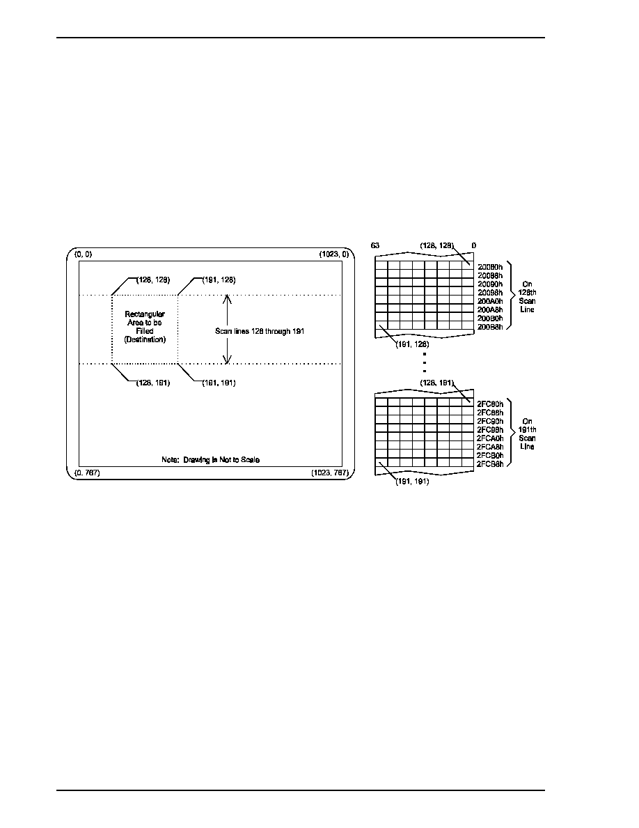
E-18
BitBLT Operation
&+,36
Æ
69000 Databook
Subject to Change Without Notice
Revision 1.3 8/31/98
BitBLT Programming Examples
Pattern Fill -- A Very Simple BitBLT
In this example, a rectangular area on the screen is to be filled with a color pattern stored as pattern data
in off-screen memory. The screen has a resolution of 1024x768 and the graphics system has been set to
a color depth of 8 bits per pixel.
As shown in Figure E-13, the rectangular area to be filled has its upper left-hand corner at coordinates (128,
128) and its lower right-hand corner at coordinates (191, 191). These coordinates define a rectangle
covering 64 scan lines, each scan line's worth of which is 64 pixels in length -- in other words, an array of
64x64 pixels. Presuming that the pixel at coordinates (0, 0) corresponds to the byte at address 00h in the
frame buffer memory, the pixel at (128, 128) corresponds to the byte at address 20080h.
Figure E-13: On-Screen Destination for Example Pattern Fill BitBLT
As shown in Figure E-14, the pattern data occupies 64 bytes starting at address 100000h. As always, the
pattern data represents an 8x8 array of pixels.
Before programming the BitBLT engine in any way, bit 0 of the BitBLT Configuration Register (XR20) or bit
31 of the BitBLT Control Register (BR04) should be checked to see if the BitBLT engine is currently busy.
The BitBLT engine should not be programmed in any way until all BitBLT operations are complete and the
BitBLT engine is idle. Once the BitBLT engine is idle, programming the BitBLT engine for the operation in
this example should begin by making sure that the BitBLT Configuration Register (XR20) is set to 00h, in
order to specify a color depth of 8 bits per pixel and enable normal operation. Alternatively, if bit 23 of the
BitBLT Control Register (BR04) is set to 1, then the color depth of the BitBLT engine may be set to 8 bits
per pixel by setting bits 25 and 24 of the same register to 0, although it is still necessary to ensure that at
least bit 1 of the BitBLT Configuration Register is set to 0 to enable normal operation.
The BitBLT Control Register (BR04) is used to select the features to be used in this BitBLT operation, and
must be programmed carefully. Bits 22-20 should be set to 0 to select the top-most horizontal row of the
pattern as the starting row used in drawing the pattern starting with the top-most scan line covered by the
destination. Since actual pattern data will be used, bit 19 should be set to 0. The pattern data is in color
with a color depth of 8 bits per pixel, so bits 18 and 17 should also be set to 0. Since this BitBLT operation

BitBLT Operation
E-19
&+,36
Æ
69000 Databook
Subject to Change Without Notice
Revision 1.3 8/31/98
does not use per-pixel write-masking, bits 16-13 should be set to 0. Bit 12 should be set to 0 to ensure that
the settings in the Monochrome Source Control Register (BR03) will have no effect on this BitBLT operation.
Bit 11 should be set to 0 to configure the BitBLT engine for a destination within the frame buffer. The setting
of bits 10-8 do not affect this BitBLT operation, since source data is not used. Therefore, these bits might
as well be set to zero as a default. Finally, bits 7-0 should be programmed with the 8-bit value of F0h to
select the bit-wise logical operation in which a simple copy of the pattern data to the destination takes place.
Selecting this bit-wise operation in which no source data is used as an input causes the BitBLT engine to
automatically forego either reading source data from the frame buffer or waiting for the host CPU to provide
it.
Bits 28-16 of the Source and Destination Offset Register (BR00) must be programmed with number of bytes
in the interval from the start of one scan line's worth of destination data to the next. Since the color depth
is 8 bits per pixel and the horizontal resolution of the display is 1024, the value to be programmed into these
bits is 400h, which is equal to the decimal value of 1024. Since this BitBLT operation does not use source
data, the BitBLT engine ignores bits 12-0.
Bits 22-3 of the Pattern Address Register (BR05) must be programmed with the address of the pattern data.
This address is specified as an offset from the beginning of the frame buffer where the pattern data begins.
In this case, the address is 100000h.
Similarly, bits 22-0 of the Destination Address Register (BR07) must be programmed with the address of
the destination, i.e., the offset from the beginning of the frame buffer of the byte at the destination that will
be written to first. In this case, the address is 20080h, which corresponds to the byte representing the pixel
at coordinates (128, 128).
Figure E-14: Pattern Data for Example Pattern Fill BitBLT
This BitBLT operation does not use the values in the Pattern/Source Expansion Background Color Register
(BR01), the Pattern/Source Expansion Foreground Color Register (BR02), the Monochrome Source Control
Register (BR03), the Source Address Register (BR06), the Source Expansion Background Color Register
(BR09), or the Source Expansion Foreground Color Register (BR0A).
The Destination Width and Height Register (BR08) must be programmed with values that describe to the
BitBLT engine the 64x64 pixel size of the destination location. Bits 28-16 should be set to carry the value
of 40h, indicating that the destination location covers 64 scan lines. Bits 12-0 should be set to carry the
value of 40h, indicating that each scan line's worth of destination data occupies 64 bytes. The act of writing
a non-zero value for the height to the Destination Width and Height Register (BR08) is what signals the
BitBLT engine to begin performing this BitBLT operation. Therefore, it is important that all other
programming of the BitBLT registers be completed before this is done.

E-20
BitBLT Operation
&+,36
Æ
69000 Databook
Subject to Change Without Notice
Revision 1.3 8/31/98
Figure E-15 shows the end result of performing this BitBLT operation. The 8x8 pattern has been repeatedly
copied ("tiled") into the entire 64x64 area at the destination.
Figure E-15: Results of Example Pattern Fill BitBLT
Drawing Characters Using a Font Stored in System Memory
In this example BitBLT operation, a lowercase letter "f" is to be drawn in black on a display with a gray
background. The resolution of the display is 1024x768, and the graphics system has been set to a color
depth of 8 bits per pixel. Figure E-16 shows the display on which this letter "f" is to be drawn. As shown in
this figure, the entire display is shaded gray. The letter "f" is to be drawn into an 8x8 region on the display
with the upper left-hand corner at the coordinates (128, 128).

BitBLT Operation
E-21
&+,36
Æ
69000 Databook
Subject to Change Without Notice
Revision 1.3 8/31/98
Figure E-17 shows both the 8x8 pattern making up the letter "f" and how it is represented somewhere in the
host's system memory -- the actual address in system memory is not important. The letter "f" is represented
in system memory by a block of monochrome graphics data that occupies 8 bytes. Each byte carries the 8
bits needed to represent the 8 pixels in each scan line's worth of this graphics data. This type of pattern is
often used to store character fonts in system memory.
Figure E-16: On-Screen Destination for Example Character Drawing BitBLT
Figure E- 17: Source Data in System Memory for Example Character Drawing BitBLT
During this BitBLT operation, the host CPU will read this representation of the letter "f" from system memory,
and write it to the BitBLT engine by performing memory writes to the BitBLT data port. The BitBLT engine
will receive this data from the host CPU and use it as the source data for this BitBLT operation. The BitBLT
engine will be set to the same color depth as the graphics system ( 8 bits per pixel, in this case. Since the
source data in this BitBLT operation is monochrome, color expansion must be used to convert it to an 8 bpp
color depth. To ensure that the gray background behind this letter "f" is preserved, per-pixel write masking
will be performed, using the monochrome source data as the pixel mask.
As in the example of the pattern fill BitBLT operation, the first step before programming the BitBLT engine
in any way is to check either bit 0 of the BitBLT Configuration Register (XR20) or bit 31 of the BitBLT Control
Register (BR04) to see if the BitBLT engine is currently busy. After waiting until the BitBLT engine is idle,

E-22
BitBLT Operation
&+,36
Æ
69000 Databook
Subject to Change Without Notice
Revision 1.3 8/31/98
programming the BitBLT engine should begin by making sure that the BitBLT Configuration Register (XR20)
is set to 00h, to specify a color depth of 8 bits per pixel and to enable normal operation. Alternatively, if bit
23 of the BitBLT Control Register (BR04) is set to 1, then the color depth of the BitBLT engine may be set
to 8 bits per pixel by setting bits 25 and 24 of the same register to 0, although it is still necessary to ensure
that at least bit 1 of the BitBLT Configuration Register is set to 0 to enable normal operation.
The BitBLT Control Register (BR04) is used to select the features to be used in this BitBLT operation. Since
pattern data is not required for this operation, the BitBLT engine will ignore bits 22-17, however as a default,
these bits can be set to 0. Since monochrome source data will be used as the pixel mask for the per-pixel
write-masking operation used in this BitBLT operation, bits 16-14 must be set to 0, while bit 13 should be
set to 1. Bit 12 should be set to 1, to specify that the data source is monochrome. Bit 11 should be set to
0 to configure the BitBLT engine for a destination within the frame buffer. Bit 10 should be set to 1, to
indicate that the source data will be provided by the host CPU. Presuming that the host CPU will provide
the source data starting with the byte that carries the left-most pixel on the top-most scan line's worth of the
source data, bits 9 and 8 should both be set to 0. Finally, bits 7-0 should be programmed with the 8-bit value
CCh to select the bit-wise logical operation that simply copies the source data to the destination. Selecting
this bit-wise operation in which no pattern data is used as an input, causes the BitBLT engine to
automatically forego reading pattern data from the frame buffer.
Unlike the earlier example of a pattern fill BitBLT operation where the Monochrome Source Control Register
(BR03) was entirely ignored, several features of this register will be used in this BitBLT operation. Bit 27 of
this register will be set to 0, thereby selecting the Pattern/Source Expansion Foreground Color Register
(BR02) to specify the color with which the letter "f" will be drawn. This example assumes that the source
data will be sent in one quadword that will be quadword-aligned. Therefore, bits 26, 25, and 24, which
specify alignment should be set to 1, 0, and 1, respectively. Since clipping will not be performed in this
BitBLT operation, bits 21-16, 13-8, and 5-0 should all be set to 0.
Bits 28-16 of the Source and Destination Offset Register (BR00) must be programmed with a value equal
to number of bytes in the interval between the first bytes of each adjacent scan line's worth of destination
data. Since the color depth is 8 bits per pixel and the horizontal resolution of the display is 1024 pixels, the
value to be programmed into these bits is 400h, which is equal to the decimal value of 1024. Since the
source data used in this BitBLT operation is monochrome, the BitBLT engine will not use a byte-oriented
offset value for the source data. Therefore, bits 12-0 will be ignored.
Since the source data is monochrome, color expansion is required to convert it to color with a color depth
of 8 bits per pixel. Since the Pattern/Source Expansion Foreground Color Register (BR02) was selected to
specify the foreground color of black to be used in drawing the letter "f", this register must be programmed
with the value for that color. With the graphics system set for a color depth of 8 bits per pixel, the actual
colors are specified in the RAMDAC palette, and the 8 bits stored in the frame buffer for each pixel actually
specify the index used to select a color from that palette. This example assumes that the color specified at
index 00h in the palette is black, and therefore bits 7-0 of this register should be set to 00h to select black
as the foreground color. The BitBLT engine ignores bits 23-8 of this register because the selected color
depth is 8 bits per pixel. Even though the color expansion being performed on the source data normally
requires that both the foreground and background colors be specified, the value used to specify the
background color is not important in this example. Per-pixel write-masking is being performed with the
monochrome source data as the pixel mask, which means that none of the pixels in the source data that will
be converted to the background color will ever be written to the destination. Since these pixels will never
be seen, the value programmed into the Pattern/Source Expansion Background Color Register (BR01) to
specify a background color is not important.
Since the CPU is providing the source data, and this source data is monochrome, the BitBLT engine ignores
all of bits 22-0 of the Source Address Register (BR06).
Bits 22-0 of the Destination Address Register (BR07) must be programmed with the address of the
destination data. This address is specified as an offset from the start of the frame buffer of the pixel at the
destination that will be written to first. In this case, the address is 20080h, which corresponds to the byte
representing the pixel at coordinates (128, 128).

BitBLT Operation
E-23
&+,36
Æ
69000 Databook
Subject to Change Without Notice
Revision 1.3 8/31/98
This BitBLT operation does not use the values in the Pattern Address Register (BR05), the Source
Expansion Background Color Register (BR09), or the Source Expansion Foreground Color Register
(BR0A).
The Destination Width and Height Register (BR08) must be programmed with values that describe to the
BitBLT engine the 8x8 pixel size of the destination location. Bits 28-16 should be set to carry the value of
8h, indicating that the destination location covers 8 scan lines. Bits 12-0 should be set to carry the value of
8h, indicating that each scan line's worth of destination data occupies 8 bytes. As mentioned in the previous
example, the act of writing a non-zero value for the height to the Destination Width and Height Register
(BR08) provides the BitBLT engine with the signal to begin performing this BitBLT operation. Therefore, it
is important that all other programming of the BitBLT engine registers be completed before this is done.
Figure E-18 shows the end result of performing this BitBLT operation. Only the pixels that form part of the
actual letter "f" have been drawn into the 8x8 destination location on the display, leaving the other pixels
within the destination with their original gray color.
Figure E-18: Results of Example Character Drawing BitBLT

E-24
BitBLT Operation
&+,36
Æ
69000 Databook
Subject to Change Without Notice
Revision 1.3 8/31/98

&+,36
Æ
69000 Databook
Subject to Change Without Notice
Preliminary Rev. 1.3 8/31/98
Chips and Technologies, Inc.
a subsidiary of Intel Corporation
Title:
69000 Data Book
2950 Zanker Road
Publication No.:
DB181.3
San Jose, California 95134
Stock No.:
010-181-003
Phone: 408-434-0600
Revision No.:
1.3
FAX: 408-894-2077
Date:
08/31/98